A Compact Readout Electronics Based on Current Amplifier for Micromegas Detector
in Muon Image
Abstract
Muon imaging technology is an innovative imaging technique that can be applied in volcano imaging, heavy nuclear material detection, and archaeological research. The Micromegas detector is a promising choice for muon imaging due to its high spatial resolution and large area. However, the large number of readout channels poses a challenge for electronics. In this paper, a compact front-end electronics (FEE) for reading Micromegas detectors is presented. The electronics use a current-based readout chip, ADAS1128, which integrates 128 current amplifiers for multi-channel charge measurement. After noise and calibration tests, detector energy resolution tests were performed using 5.9 keV X-rays. The X-ray full energy peak and Ar escape peak can be observed; the energy resolution of the full energy peak is about 20.23%@5.9 keV. Additionally, a muon image system was set up to verify the imaging capacity of Micromegas detectors. Test results show that the spatial resolution of the system is better than 200 m. The muon image system can reconstruct the boundaries for objects with a size of 2 cm.
Index Terms:
Current amplifiers, Micromegas detector, Readout electronicsI Introduction
Muon imaging is a new type of imaging technology divided into three categories: scattering, transmission, and muon metrology. Compared with other imaging methods, it has the advantages of low cost, detection of large-scale objects, non-destructive detection, and safety. Currently, muon imaging technology has been used in the fields of volcano imaging [1], heavy nuclear material detection [2], and archaeological research [3]. Because of the low flux of natural cosmic ray muons, muon imaging requires large-area detectors to meet the demand for high-precision, short-time imaging. In recent years, much progress has been made in the research of Micro-pattern Gas Detectors, especially Micromegas detectors. It has been shown that Micromegas detectors can achieve an effective area of more than 1 m 1 m [4] and a spatial resolution of less than 200 m [5]. They are suitable for conducting muon imaging studies.
The Micromegas detector used in this paper was developed by the State Key Laboratory of Nuclear Detection and Nuclear Electronics at the University of Science and Technology of China [6]. The working gas of the detector is a mixture of 93% Ar and 7% CO2. In addition, the detector is read out by crossed anode strips in both X and Y dimensions with a pitch of 400 m. The effective area of the currently recent design Micromegas detectors is 60 60 cm2 with 3000 detection units.
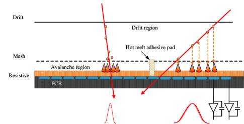
The Micromegas detector primarily comprises anode readout strips, a resistive layer, a mesh layer, a drift layer, and a gas chamber [7], as shown in Figure 1. Among them, the avalanche area is formed between the mesh layer and the resistive layer, and the drift area is formed between the drift layer and the mesh layer. The incident particles enter the detector to produce ionization in the drift region, and the electrons enter the avalanche region to generate a large number of electron-ion pairs. The electrons drift rapidly toward the anode region, inducing a fast signal on the hundred-nanosecond scale. The positive ions drift towards the mesh, inducing a slow signal on the nanosecond scale. Therefore, the signal obtained by the anode strips is composed of a faster electron signal and a slower ion signal superimposed, as shown in Figure 2 [8].
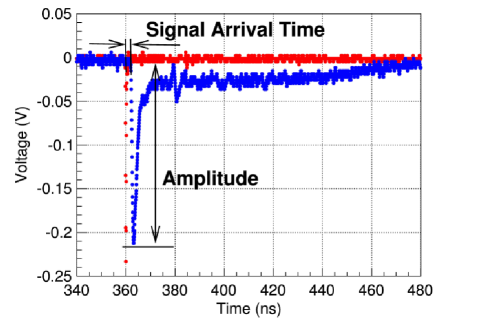
The pulse width of the output signal from the anode strips of the Micromegas detector is approximately 100 ns, and the output charge ranges from a few to a few hundred fC. To accurately measure the information of charged particle incidents on the Micromegas detector and to perform readout of a large number of detector units, the electronics system needs to fulfill the requirements of low noise and high integration. The main ASIC chips currently used to read out Micromegas detectors are the digital chip MICROROC [9] designed by the French Omega group and the analog chip AGET (Asic for General Electronics for Tpc) [10] developed by the French Scalay Laboratory. The main working principle of both chips is based on shaping and amplifying the detector signal using charge-sensitive amplifiers before further processing and readout.
A large number of electronic channels are required for muon imaging studies using large-area, high-resolution Micromegas detectors. A compact front-end electronics based on the current readout was designed to reduce the electronic’s power consumption and size and improve the electronics integration.
II Electronics Readout Design
II-A Introduction of the ADAS1128
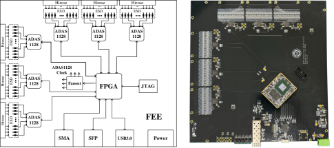
To meet the high integration design requirement, FEE adopts the current readout chip ADAS1128 [11] designed by ADI. Its internal structure is shown in Figure 3, and the chip is composed of 128 current integration amplifiers, sample circuits, two 24-bit resolution analog-to-digital converters (ADCs), and digital processing parts. The input signal from each channel will be integrated over a specified period, after which it will be sampled. Next, the sampled values of the 128 channels, divided into groups of 64, are sent to two 24-bit resolution ADCs for analog-to-digital conversion. Finally, the measurement results of all channels are output on a single low voltage differential signaling (LVDS) self-clocking serial interface according to the readout timing. In addition, the chip also includes two 24-bit configuration registers, a temperature sensor, and a reference buffer module.
The chip supports Serial Peripheral Interface configuration (SPI), which allows daisy-chained communication, significantly reducing the need for external hardware and meeting the need for highly integrated designs in electronics. The chip features an adjustable measurement charge range, with a maximum dynamic range of -660.17 fC to 32.23 pC at the highest sampling rate of 19.7 kSPS (integration time of 50.7s). In our situation, only the negative range is used. According to the anode strip signals of the Micromegas above, the integration time for reading out the detector signal is much shorter than that of the chip. Nevertheless, under the premise of medium to low event rates, this article attempts to use the highly integrated ADAS1128 chip to read out the Micromegas and demonstrates the feasibility of this readout scheme.

II-B Design of FEE
The initial stage FEE design for the readout Micromegas detector was completed as shown in Figure 4. FEE mainly consists of the detector signal readout, data acquisition, and power supply modules. The sensitive area of the Micromegas detector is 15 cm 15 cm, with strip readout in the X and Y dimensions. There are 384 channels for detector signals in each dimension. The detector signal readout module integrates 6 ADAS1128 chips, with each chip’s charge input stage connected to electrostatic discharge (ESD) protection circuits to prevent damage to the electronic channels caused by the discharge. Detector signals enter the board via high-density connectors, pass through ESD protection circuits, and are sent to the ADAS1128 for analog-to-digital conversion. The data acquisition module mainly consists of an FPGA core board, optical fiber communication interface, and universal serial bus (USB) 3.0 interface. Its primary functions include configuring the ADAS1128 chip, collecting chip data, and facilitating communication with the data acquisition (DAQ) board or host computer.
The main control chip on the field-programmable gate array (FPGA) core board is the Aritix-7 chip produced by Xilinx. The core board has onboard power modules, double data rate synchronous dynamic random access memory, quad serial peripheral interface flash, a 50MHz crystal oscillator, and other devices. A large number of I/O ports are reserved on the board, connected to the FEE board via four 0.8mm-pitch connectors. The optical fiber communication interface module is designed with a clock recovery chip, ADN2817 [12], which can extract clock and serial data from the optical fiber link. The recovered clock is input into the FPGA clock management unit to generate the required logic control clock. At the same time, the serial data is input into the FPGA to complete serial-to-parallel conversion and command parsing. The USB 3.0 module uses the CYUSB3014 [13] chip designed by Cypress, with a data transfer speed of up to 350 MBps, facilitating single-board test.
II-C Introduction of Data Acquisition Board
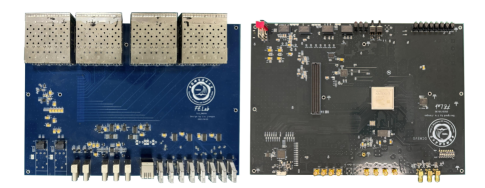
The back-end electronics utilize the previously designed DAQ board [14], as shown in Figure 5. It consists of an extension board for constructing the front-end chain and a mainboard for controlling communication. The DAQ board communicates with FEEs using fiber optics with custom protocols [15]. The DAQ board sends triggers, clocks, and control commands to the FEEs while receiving the data from FEEs and uploading it to a host computer via a USB 3.0 interface.
II-D Design of Readout Electronics System
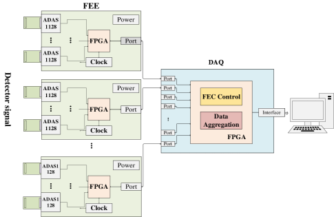
To improve system scalability and ensure accurate measurement of detector signals, the entire readout electronics system is divided into FEEs and DAQ. FEEs amplify and digitize detector signals before transmitting them to DAQ. DAQ further processes and stores the data. Considering the complex environment and external interference that the cosmic ray muon imaging test will encounter, communication between FEEs and DAQ uses optical fiber interfaces. The optical fiber interface communication not only reduces noise interference from DAQ to FEEs but also enables communication over distances of several kilometers. Based on existing research, the fiber communication scheme using standard LVDS pins is sufficient to meet the data rate requirements for muon imaging and dramatically reduces the design requirements for DAQ. The architecture of the readout electronics system is shown in Figure 6.
II-E Functional Design of Electronics Systems
The functions of FEE mainly include ASIC configuration, ASIC data readout, data filtering, data packaging, data decoding, and command parsing. The FEE first needs to configure the chip through the SPI interface, including integration time and dynamic range, to achieve signal readout from the chip. Then, based on the control signals of the chip, the FEE implements serial output of data from 128 channels. After controlling the chip data readout, the FEE needs to filter the data based on the threshold to compress the data volume. In addition, the FEE needs to upload the over-threshold flag signal to the DAQ. After judging the flag signals, DAQ sends trigger signals to FEE. At this point, FEE packages and uploads the data of over-threshold channels to DAQ.
The functions of DAQ mainly include data link encoding, trigger generation, data reception, command parsing, and USB 3.0 control. The optical fiber communication link between the front-end and back-end electronics is divided into three data channels (channels a, b, and c). Channel a transmits trigger signals, with DAQ issuing trigger signals to FEE. Additionally, FEE also transmits over-threshold flag signals through channel a. DAQ transmits configuration information to the FEE through channel b, thereby completing the configuration and channel threshold settings of the ADAS1128 chip. FEE uploads data packets to DAQ via channel c. The system functions diagram is shown in Figure 7.

The electronics system operates in two trigger modes: self-trigger and external-trigger. FEEs digitize the signals from each channel of the detectors at each integration time and then feed them into the data filtering module for threshold judgment. When the chip detects that the signals from at least two channels exceed the threshold, the over-threshold flag signal of the chip is set to 1; otherwise, it remains at 0. Each layer of FEE transmits over-threshold judgment signals to DAQ via optical fibers. The trigger generation module of DAQ performs logical judgments on the flag signals. In this trigger mode, the event is deemed valid if both the number of x-dimension over-threshold layers and the number of y-dimension over-threshold layers are detected to exceed the predetermined value. At this point, the trigger signal is sent to all FEEs. The trigger generation conditions can be flexibly modified according to experimental requirements. When operating in external trigger mode, DAQ sends triggers to all FEEs, and FEEs upload the data to DAQ.
II-F Muon Image System
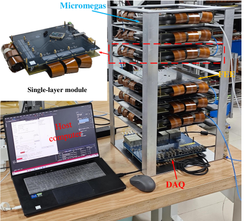
The muon image system consists of 6 layers of Micromegas detectors, 6 FEE boards, a DAQ board, a Host computer, and high-voltage connectors, as shown in Figure 8. Each FEE is connected to a 15 cm 15 cm Micromegas detector through flexible boards, and they are integrated as a single module. During the testing, the entire system operates in a self-trigger mode. The anode potential of the detectors is grounded, and the wire mesh voltage and drift electrode voltage are set to -550 V and -678 V, respectively.
III Experimental Results
III-A Pedestal and Noise Test
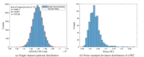
Pedestal and noise tests are performed on FEE under floating input conditions. The integration time of the chip is 50.7 s, and the dynamic range of the negative charge is -77.97 0 fC. Figure 9(a) shows the pedestal statistics for a single electronics channel of the ADAS1128 chip. The pedestal statistical results obtained for each channel are fitted using a normal distribution. The average value of the fitting result is the chip’s pedestal, and its standard deviation is the chip’s equivalent input noise. Channel thresholds can be set based on the mean and standard deviation of the pedestal statistics. Figure 9(b) shows the statistics of the equivalent input noise for all channels, with 95% of the channels of the 6 ADAS1128 chips having a noise of less than 0.68 fC (based on the following calibration results).
III-B Calibration Test
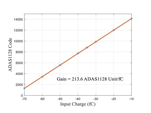
In the calibration test, the voltage signal is converted to a current signal by generating a step-down signal and sending it to a 1pF capacitor in series. Figure 10 shows the calibration results for channel No.25 within an input range of -77.97 to 0 fC. The conversion relationship between ADC code value and charge is Code = 213.6 * Charge + 16365. The test results reveal that the integral non-linearity of linear calibration for 128 channels is 2.7%.
III-C Test with an X-Ray Source
Detector energy resolution tests using radioactive source to verify FEE readout of Micromegas detector anode strip signals. Figure 11 is the graph of the test results of the radioactive source, with the hit diagram in Figure 11(a) and the energy spectrum in Figure 11(b). The X-ray full energy peak and the Ar escape peak can be clearly observed from the Figure 11(b). After the Gaussian fitting of the full energy peak and the escape peak, respectively, it can be calculated that the peak position of the full energy peak is about 389.3 fC, with an energy resolution (FWHM, Full Width at Half Maximum) of 20.23%@5.9keV. The peak position of the escape peak is about 186.7 fC, and the ratio of the full energy peak to the escape peak is 2.09:1.
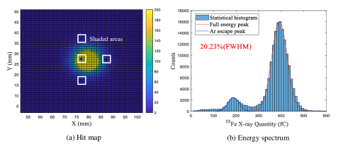
There are shaded areas in the hit diagram. Based on the analysis, the hot melt adhesive pad between the detector resistive electrode and the mesh electrode blocks the downward drifting electrons, thus preventing the electrons from drifting into the avalanche region. By slightly shifting the position of the radioactive source left and right, as shown in Figure 12, it can be seen that the position of the shadowed area is fixed. The shadowed region observed in the hit map is attributed to the dead region caused by the arrangement of thermal adhesive pads in the detector.

III-D Cosmic Ray Energy Deposition Result
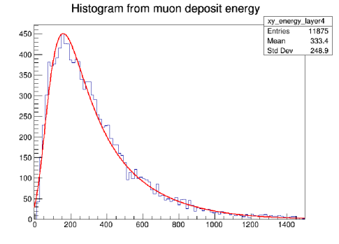
Since the charge center of gravity method is used in the cosmic ray muon test to reconstruct the muon track, the response of the cosmic ray muon’s energy deposited in the Micromegas detector is first tested. Each cosmic ray event generates induction signals on the anode readout strips in the X and Y dimensions. The charge in each dimension is separately calculated using the charge centroid method, and then the charges from the two dimensions are summed to obtain the cosmic ray energy deposition spectrum, as shown in Figure 13. From the energy spectrum, the charge distribution mainly follows the Landau distribution. After performing a Landau-Gaussian convolution fit using ROOT, the peak value is approximately 149.94 fC.
III-E Spatial Resolution Result
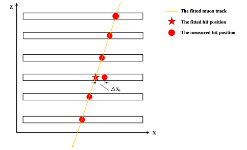
The core of the muon imaging experiment is the measurement of tracks. The method for calculating the spatial resolution of the muon track system is shown in Figure 14, with an example of calculating the spatial resolution of the i-layer. Since the amount of material inside the gas detector is tiny, the muon track passing through the detector can be regarded as a straight line. By using the hit positions of the other five layers of detectors for linear fitting, the fitted hit position xfit of the i-layer detector can be obtained. At this time, the difference between the measured hit position by FEE and the linearly fitted hit position, xi, is obtained, that is, xi=xhit-xfit. By statistically analyzing a large number of muon tracks, the distribution of xi is obtained, and the standard deviation ( xi) of the distribution is the position resolution of the layer detector. Considering that the position fluctuation caused by linear fitting and the fluctuation in the hit position of each layer detector is independent, it can be derived that 2 ( xi )= 2 (xfit )+ 2 (xhit).
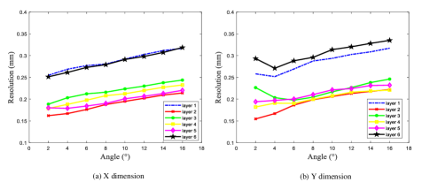
The spatial resolution of the Micromegas detector in the X and Y directions is shown in Figure 15. When calculating instances from different angles separately, the uncertainty in the initial ionization position increases as the incident angle of the muon increases[16]. The detectors located on the outer side of the track system, being farther away from the fitting center, will amplify small deviations in the fitting. Therefore, their spatial resolution is relatively worse than the inner side’s detectors. For 0 5∘ incident muons, the spatial resolution of the detector is better than 200 m.
III-F Efficiency Result
The efficiency of the target layer is obtained by inverting the hit information of the detectors in other layers, taking the efficiency of the i-layer detector as an example. First, set two counters, Nhit/i and Ntotal, representing the events with hits in the i-layer and the total number of events, respectively. Efficiency calculation is set with a maximum allowable deviation x. If the actual hit position found for an event in the i-layer falls within the spatial range of xx, then the event is a true and effective hit event. In this case, Nhit/i + 1. After traversing all instances, the efficiency of the i-layer detector is calculated as Nhit/i/Ntotal. When the maximum deviation x is set to 10 times the spatial resolution, the detection efficiency in the X and Y dimensions of detectors is shown in Table I. The result shows that Most of the 6-layer Micromegas detector’s efficiency is over 95%.
| layer-1 | layer-2 | layer-3 | layer-4 | layer-5 | layer-6 | |
|---|---|---|---|---|---|---|
| X | 96.92% | 98.73% | 98.11% | 98.29% | 98.79% | 97.31% |
| Y | 91.67% | 97.65% | 93.81% | 97.91% | 96.64% | 96.58% |
III-G Muon Scattering Imaging Result
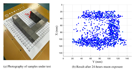
The spatial resolution and efficiency tests described above indicated that the system meets the imaging requirements. Therefore, the muon scattering imaging tests were carried out. Figure 16 shows the results of imaging a tungsten material with a minimum width of 2 cm and a thickness of 4 cm, with the tungsten block posed in the shape of . After accumulating 24 hours of test data, the imaging results were reconstructed using the Point of Closest Approach (PoCA) algorithm incorporating a k-Nearest Neighbors (k-NN) algorithm[14]. The test result shows that the muon image system can reconstruct the boundaries for objects with a size of 2 cm.
IV Conclusion and Discussion
In this study, a high-integration front-end electronics with 768 channels based on the current readout chip ADAS1128 was designed and implemented, suitable for reading out Micromegas detectors. The gain of charge measurement is about 213.6 Code/fC in the dynamic range of -77.97 0 fC. The integration nonlinearity is 2.7%, and the noise is less than 0.68 fC. Next, a 5.9 keV X-ray energy resolution test was performed to verify the readout capability of the FEE for the anode strip signal of the Micromegas detector. The results of the radioactive source test show that the energy resolution of the Micromegas detector for 5.9 keV X-rays is approximately 20.23% (FWHM). Additionally, a muon image system was set up to verify the imaging capacity of Micromegas detectors. The muon track test results indicate that for muons with 0 5∘ incidence, the spatial resolution of the system is better than 200 m. The muon scattering imaging results show that the muon image system can reconstruct the boundaries for objects with a size of 2 cm.
The FEE described in this paper can be used to read out Micromegas detectors for muon image in single particle measurement mode. Current research and development efforts are progressing towards muon imaging using large-area Micromegas detectors. In future work, we will improve front-end electronics to read out larger area Micromegas detectors. In addition, the clustering algorithm will be introduced to optimize the reconstruction results of the image further based on the PoCA algorithm.
References
- [1] K. Nagamine, M. Iwasaki, K. Shimomura, and K. Ishida, “Method of probing inner-structure of geophysical substance with the horizontal cosmic-ray muons and possible application to volcanic eruption prediction,” Nuclear Instruments and Methods in Physics Research Section A: Accelerators, Spectrometers, Detectors and Associated Equipment, vol. 356, no. 2–3, pp. 585–595, Mar. 1995, doi: 10.1016/0168-9002(94)01169-9.
- [2] P. Baesso, D. Cussans, C. Thomay, and J. Velthuis, “Toward a RPC-based muon image system for cargo containers.,” J. Inst., vol. 9, no. 10, pp. C10041–C10041, Oct. 2014, doi: 10.1088/1748-0221/9/10/C10041.
- [3] K. Morishima et al., “Discovery of a big void in Khufu’s Pyramid by observation of cosmic-ray muons,” Nature, vol. 552, no. 7685, pp. 386–390, Dec. 2017, doi: 10.1038/nature24647.
- [4] M. Iodice, “Performance studies of MicroMegas for the ATLAS experiment,” J. Inst., vol. 9, no. 01, pp. C01017–C01017, Jan. 2014, doi: 10.1088/1748-0221/9/01/C01017.
- [5] J. Wotschack,“THE DEVELOPMENT OF LARGE-AREA MICROMEGAS DETECTORS FOR THE ATLAS UPGRADE,” Mod. Phys. Lett. A, vol. 28, no. 13, p. 1340020, Apr. 2013, doi: 10.1142/S0217732313400208.
- [6] J. Feng et al., “A thermal bonding method for manufacturing Micromegas detectors,” Nuclear Instruments and Methods in Physics Research Section A: Accelerators, Spectrometers, Detectors and Associated Equipment, vol. 989, p. 164958, Feb. 2021, doi: 10.1016/j.nima.2020.164958.
- [7] Y. Giomataris, Ph. Rebourgeard, J. P. Robert, and G. Charpak,“MICROMEGAS: a high-granularity position-sensitive gaseous detector for high particle-flux environments,” Nuclear Instruments and Methods in Physics Research Section A: Accelerators, Spectrometers, Detectors and Associated Equipment, vol. 376, no. 1, pp. 29–35, Jun. 1996, doi: 10.1016/0168-9002(96)00175-1.
- [8] J. Bortfeldt et al., “PICOSEC: Charged particle timing at sub-25 picosecond precision with a Micromegas based detector,” Nuclear Instruments and Methods in Physics Research Section A: Accelerators, Spectrometers, Detectors and Associated Equipment, vol. 903, pp. 317–325, Sep. 2018, doi: 10.1016/j.nima.2018.04.033.
- [9] C. Adloff et al., “MICROROC: MICRO-mesh gaseous structure Read-Out Chip,” Journal of Instrumentation, vol. 7, p. C01029, Jan. 2012, doi: 10.1088/1748-0221/7/01/C01029.
- [10] S. Anvar et al., “AGET, the GET front-end ASIC, for the readout of the Time Projection Chambers used in nuclear physic experiments,” in 2011 IEEE Nuclear Science Symposium Conference Record, Oct. 2011, pp. 745–749. doi: 10.1109/NSSMIC.2011.6154095.
- [11] Analog Devices, Inc. 128-Channel, 24-Bit Current-to-Digital ADC ADAS1128. Analog Devices, Inc., 2010. https://www.analog.com/cn/products/adas1128.html.
- [12] I. Exceeds, L. Programmable, F. Channel, and H. GbE, “Continuous rate 10 Mbps to 2.7 Gbps clock and data recovery ics data sheet adn2817/adn2818.”
- [13] C. S. Corporation, “Cyusb301x cyusb201x ez-usb fx3 superspeed usb controller,” https://www.cypress.com/documentation/other-resources/cyusb301x-cyusb201x-ez-usb-fx3-superspeed-usb-controller, 2016.
- [14] Y. Wang et al., “A High Spatial Resolution Muon Tomography Prototype System Based on Micromegas Detector,” IEEE Trans. Nucl. Sci., vol. 69, no. 1, pp. 78–85, Jan. 2022, doi: 10.1109/TNS.2021.3137415.
- [15] C. Li, C. Q. Feng, D. Y. Zhu, S. B. Liu, and Q. An, “An optical fiber-based flexible readout system for micro-pattern gas detectors,” J. Inst., vol. 13, no. 04, pp. P04013–P04013, Apr. 2018, doi: 10.1088/1748-0221/13/04/P04013.
- [16] P. Iengo, “Performance studies of Micromegas detectors for the ATLAS experiment,” in Proceedings of The European Physical Society Conference on High Energy Physics — PoS(EPS-HEP 2013), Stockholm, Sweden: Sissa Medialab, Mar. 2014, p. 080. doi: 10.22323/1.180.0080.