[1]\fnmMohamed \surElKabbash \equalcontThese authors contributed equally to this work.
[1]\fnmSivan \surTrajtenberg-Mills \equalcontThese authors contributed equally to this work.
[1]\fnmDirk \surEnglund
[1]\orgdivResearch Laboratory of Electronics, \orgnameMassachusetts Institute of Technology, \orgaddress\street50 Vassar St, \cityCambridge, \postcode02139, \stateMA, \countryUSA
Metal-Optic Nanophotonic Modulators in Standard CMOS Technology
Abstract
Integrating nanophotonics with electronics promises revolutionary applications ranging from light detection and ranging (LiDAR) to holographic displays. Although semiconductor manufacturing of nanophotonics in Silicon Photonic foundries is maturing, realizing active nanophotonics in the ubiquitous bulk CMOS processes remains challenging. We introduce a fabless approach to embed active nanophotonics in bulk CMOS by co-designing the back-end-of-line metal layers for optical functionality. Without changing any of the design rules imposed by a 65 nm CMOS process, we realize plasmonic liquid crystal modulators that exhibit switching speeds 100 times faster than commercial technologies. Our approach, which embeds ’zero-change’ nanophotonics into the most ubiquitous platform for integrated electronics, democratizes fabrication of metal-optic nanophotonics, opens the path to mass production of active nanophotonic components, and overcomes major packaging challenges that have previously hindered the realization of complex metal-optic optoelectronic systems.
keywords:
Metal-Optics, Nanophotonics, CMOS Technology, Liquid Crystals1 Introduction
Nanophotonic devices are redefining the technology landscape across numerous sectors, including telecommunications[1], sensing[2], classical and quantum computing [3, 4, 5], bioengineering, and renewable energy[6, 7, 8], enabled by rapid advances in specialized optoelectronic processes such as silicon photonics [9], silicon nitride photonics [10], and lithium niobate photonics[11]. These developments, particularly in the silicon photonics area, were enabled through the development of the fabless photonics model. The fabless model, which originated in electronic integrated circuits, has significantly impacted the growth and commercialization of photonic integrated circuits[12]. By adopting this model, silicon photonics companies and researchers have leveraged existing silicon-based semiconductor manufacturing infrastructure and expertise, reducing costs and risks associated with building their own fabrication facilities and overcoming the limitations of scarce nanofabrication resources in research institutions. Fabless photonics has thereby accelerated the development and adoption of silicon photonic devices in applications such as data centers, telecommunications, and sensing.
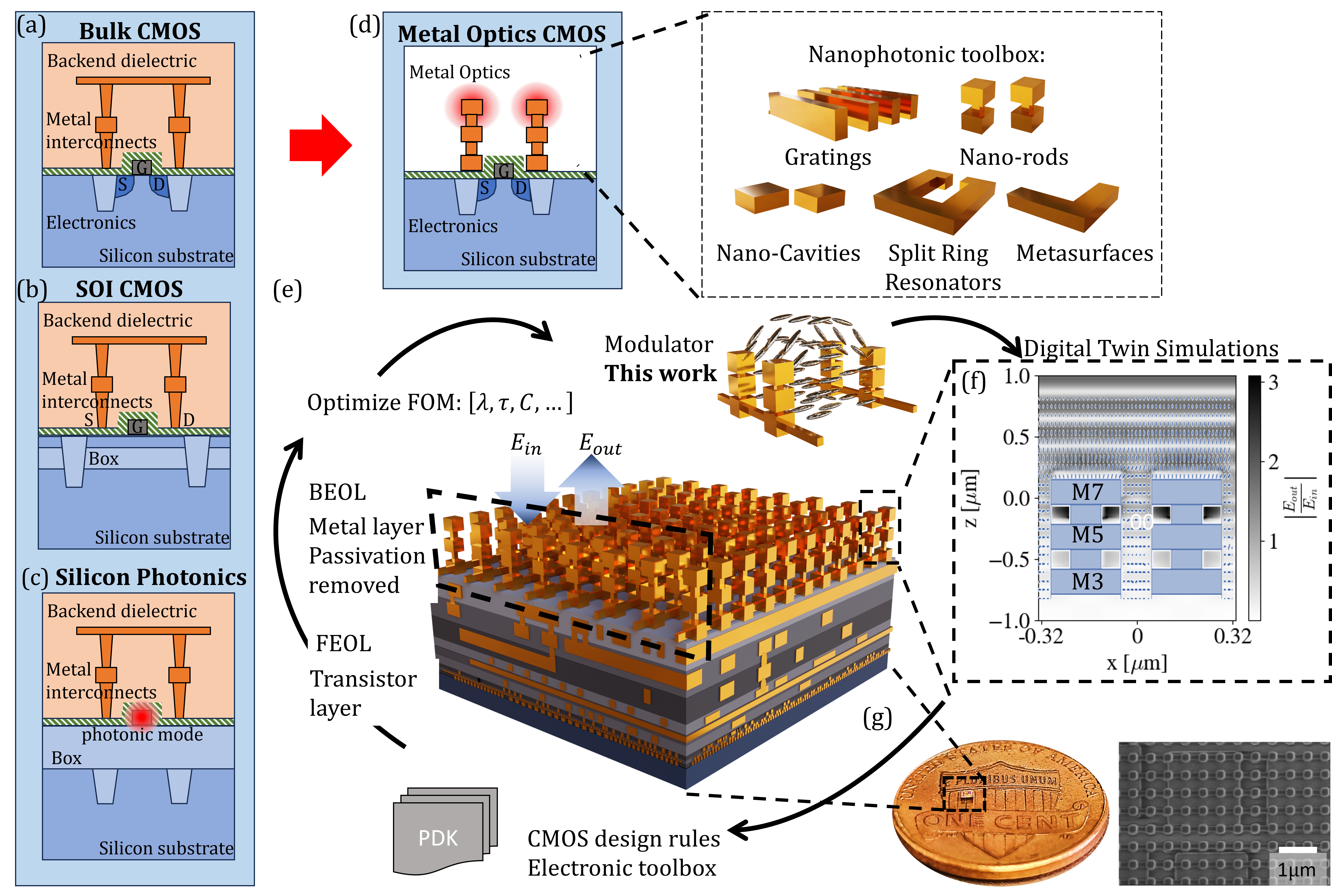
Despite this progress, an open challenge is the lack of active nanophotonic components in the majority of current semiconductor foundry processes, specifically in CMOS processes. In the bulk CMOS process, shown schematically in Fig. 1(a), the electronics and transistors in the front-end-of-the-line (FEOL) silicon layer are wired through metal layers in the back-end-of-the-line (BEOL), which are supported by a dielectric passivisation material. In silicon-on-insulator (SOI) processes, a layer of buried oxides (”box”) separates the device silicon layer from the bulk silicon substrate, Fig. 1(b). Since this is a thin layer, the top silicon cannot support a photonic mode which leaks into the bulk. Silicon Photonics, in Fig. 1(c), has a thick ”box” layer, allowing for the support of a photonic mode, but is therefore further away from the electronic device layer, making the integration with electronics difficult. In order to overcome the difficulty of co-integrating photonics with electronics in current processes, researchers have proposed specialized foundry processes (that have very limited commercial availability, and are therefore incredibly expensive), as well as methods requiring heavy post processing. Co-integration of photonics and electronics in CMOS foundries was demonstrated in silicon-on-insulator processes [13, 14, 15, 16]. In addition, specialized foundry processes were customized to create a local photonics region through etching regions in the silicon substrate and depositing an oxide fill and a polycrystalline silicon thin film [17]. However, the co-integration of photonic and electronic devices into bulk silicon CMOS foundry processes, which is by far the cheapest, has remained an outstanding challenge. Incorporating nanophotonic devices into standard bulk CMOS processes would be transformative, enabling the integration of photonic devices onto existing CMOS chips. This integration would enable numerous applications, such as LiDAR scanners with CMOS focal plane arrays, hyperspectral biosensing [18], and holographically programmable light-field imagers and displays[19].
The challenge of co-integrating nanophotonics with electronics within bulk CMOS foundry processes primarily stems from the inability of the bulk silicon layer to support photonic modes (Fig.1 a). Moreover, thin-body fully depleted silicon-on-insulator (SOI) CMOS processes cannot support photonic modes in the thin ( 20 nm) crystalline silicon layer [17](Fig.1 b). While SOI substrates have been the primary platform for the monolithic integration of photonics with CMOS (Fig.1 c), they are costly and have a limited supply chain, making them less ideal for high-volume and cost-sensitive applications. Furthermore, photonic SOI processes suffer from limitations due to thermal crosstalk and limited heat dissipation, resulting from the thicker buried oxide layer. However, a comprehensive examination of the entire CMOS chip structure (as depicted in Fig. 1) reveals that the back-end-of-the-line (BEOL) consists of multiple metal layers that serve as electrical interconnects for the semiconductor devices housed within the FEOL. These metal layers can be patterned with nano-scale resolution. Accordingly, the BEOL can be repurposed to create metal-optic or plasmonic devices that are compatible with bulk CMOS foundry processes.
In this work, we introduce a fabless model for metal-optics using commercial bulk CMOS foundry processes with zero change to the process design rules. Through careful design of the metal interconnect layers in CMOS chips, it is possible to realize most of the building blocks of metal-optic nanophotonics within the constraints of the foundry design rules (see Fig. 1). To demonstrate the potential of the fabless nanophotonics model, we co-designed several of the metal interconnect layers in 65-nanometer-transistor bulk CMOS process technology to implement both electronic and optical functionalities. Taking advantage of the three-dimensional nanofabrication capability of CMOS foundries, individual plasmonic nanoresonators are electrically interconnected to construct an active plasmonic device. Through minor post-processing, we introduce liquid crystal (LC) molecules to the plasmonic device and realize an on-chip electro-optic modulator.Several metal layers in the BEOL are designed to have multiple functionalities simultaneously: they function as alignment layers for LC molecules, as an optical resonator, and as interdigitated electrodes for the modulator. Commercial LC optical modulators exhibit a relatively long response time due to the time required for the molecules to reorient themselves under the influence of an electric field. We show that by leveraging the nanoscale resolution of the CMOS metal layers, we can realize smaller effective cell thicknesses that increase the response speed to KHz, which is two orders of magnitude faster than modern high-speed LC modulators with speeds KHz [20, 21]. The proposed CMOS nanophotonic high-speed LC modulator can find applications in telecommunications, reconfigurable optical add-drop multiplexing, optical and quantum computing, sensing and imaging, holographic displays, LiDARs, and miniaturized spectroscopy.
2 Fabless CMOS Metal-optics Approach
Fig. 1e schematically presents the proposed fabless nanophotonics approach using the BEOL of CMOS chips. A few metal layers in the BEOL of a CMOS chip are optimized to meet desired figures of merit (FOM) for their optical response, such as linear or circular retardance, photonic resonance, etc., while satisfying the design rules imposed by the CMOS foundry. In the context of optical modulators, the FOM can include the operation wavelength , the response time , the modulation contrast or others. Following the design rules, a library of nanophotonic components such as gratings, nano-antennas, nano-rods, metasurfaces, ring resonators, etc., can be created. Not all geometries satisfy the design rules of a given CMOS process. For example, some patterns generated through inverse design will not satisfy the foundry design rules [22]. The remaining metal layers are spared for wiring or connection to different electronic devices in the FEOL, such as transistors for optoelectronic control, photodiodes, CMOS photodetectors, heaters, or electromagnets. Consequently, the proposed approach can integrate nanophotonic devices with advanced electronic devices.
Depending on the foundry process used, the spatial resolution and the type of metal would differ, with general tendency of advanced processes to have more metal layers and higher spatial resolution. Due to its desirable electronic properties, wires are typically made of copper. Copper is a good plasmonic metal at the red part of the spectrum and has excellent performance in the NIR and IR spectral range [23]. Aluminum is used in older CMOS processes and in the top metal layers of most CMOS processes (the ). Aluminum is the best plasmonic metal in the UV range and has good performance across the visible spectrum. It is nearly indistinguishable in terms of optical losses from gold or silver in the NIR range [24]. Depending on the foundry process used, the spatial resolution and the type of metal would differ, with general tendency of advanced processes to have more metal layers and higher spatial resolution. Due to its desirable electronic properties, wires are typically made of copper. Copper is a good plasmonic metal at the red part of the spectrum and has excellent performance in the NIR and IR spectral range [23]. Aluminum is used in older CMOS processes and in the top metal layers of most CMOS processes (the ”Redistribution Layer” or ”Aluminum Pad Layer”). Aluminum is the best plasmonic metal in the UV range and has good performance across the visible spectrum. It is nearly indistinguishable in terms of optical losses from gold or silver in the NIR range [24].
3 Design of Liquid Crystal Metal-optic Modulator
Liquid crystal (LC) modulators are optoelectronic devices that control the intensity, phase, or polarization of light through the electro-optical properties of LC molecules [25]. They are stable, inexpensive, and commercially established with applications in displays, communication, adaptive optics, holography, and imaging. Many LC modulators rely on the electric field-induced Freedericksz transition, where LC molecules reorient under the influence of an applied electric field when the applied potential difference exceeds the threshold voltage . The time it takes LC molecules to align with the applied field is given by [26]
| (1) |
where and are the viscosity coefficient and the elastic constant of the LC, respectively, and is the LC cell thickness. Fast LC modulators are conventionally phase modulators where the acquired phase depends on the LC optical anisotropy, cell thickness, and operation wavelength. To obtain a desired phase range for a given LC molecule and operation wavelength, the cell thickness is not a design parameter. In the optical range, the cell size is on the order of a few m, which results in ms. For many applications such as imaging through scattering media [27], video holography [28], quantum tomography [29], and quantum control [11], the use of high-speed optical modulators is critical. Research on increasing the speed of LC modulators focuses on modifying the mechanical properties of the LC molecules to reduce their viscosity or threshold voltage [20, 21] which led to the development of nematic LC modulators with a response time of .
Alternatively, increasing the speed of the LC modulators by decreasing is possible when modulating a nanophotonic resonance [26, 30]. We introduce a nanophotonic LC optical modulator that exploits the modulation of a localized plasmon resonance generated in metal nanorods. The modulator design encompasses a two-dimensional array of nanorods that support localized plasmon resonances that depend on the rod height, width, and pitch [31]. The nanorod array is designed by connecting multiple metal layers (M7, M6, and M5) through vias. The individual nanorods are connected by extending a wire (width nm) that traverses across them. The wires have three simultaneous purposes: first, they act as a mechanical support for the nanrods; second, they provide an alignment layer for the LC molecules, allowing for the LCs to be drop-casted onto the sample and align along the wires without need for additional alignment layers; and finally, they act as interdegitated electrodes, supplying the potential difference and electric field for the modulator operation. We simulated the response of LC molecules embedded in the designed plasmonic structure. The LC molecules initially align parallel to the wires; however, When a bias is applied across the electrodes, the LC molecules re-orient along the fringe field which modifies the refractive index sensed by the plasmon resonance. Fig. 2(a) shows a simulation of these dynamics, without the bias (top) and with it (bottom), where a change in the orientation of the liquid crystal molecules (light blue lines) is apparent.
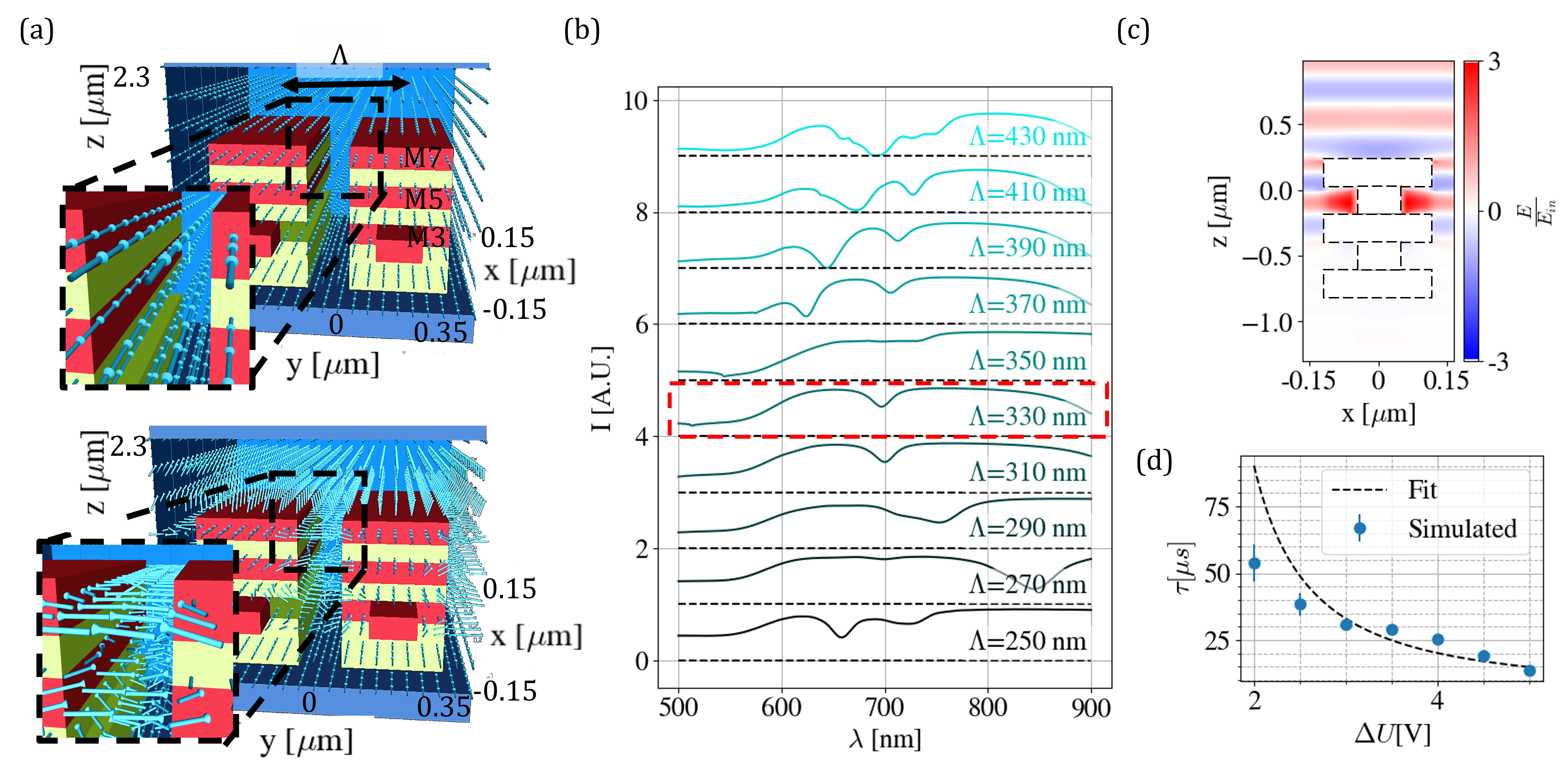
Our design targets the modulator to operate at a wavelength of 700 nm, which is of interest to quantum computing technologies [11]. We calculated the nano-rod array resonance as a function of the array’s pitch (Fig. 2(b)). A nano-rod pitch of 330 nm and a rod width of 230 nm exhibits a resonance at 700 nm. The electric field simulation of the nanorods at resonance is shown Fig. 2(C) (see Methods for details on the field simulations). In our simulations, we assumed an LC layer as a superstrate with . A field enhancement factor of 3 for the x component of the electric field occurs primarily in the region between the nanorods. The optimized nano-rod array dimensions are then incorporated into simulations of the LC dynamics (see Methods). Fig. 2(d) shows the simulated for different applied voltages. As the bias increaases, decreases and reaches 0.01380.0002 ms at . From the fit parameters we can extract the effective cell thickness (see Methods) according to Equation 1. Based on the simulated , the effective cell thickness, , is 81 11 nm.
4 Fabrication and Experimental Results
Our designed modulators were fabricated by a CMOS foundry (TSMC) in their 65-nm bulk CMOS process. The passivation layer of the as-received chips was removed through reactive ion etching (see Supplementary Materials). In Fig. 3(a), we delineate the micro- and nano-scale features of the chip. SubFig. 3(a)(i) show the chip next to a US cent coin. SubFig. 3(a)(ii) provides a view of the full CMOS chip following the removal of the passivation layer. Using scanning electron microscopy (SEM), SubFig. 3(a)(iii) and 3(a)(iv) depict nanorod devices, with different pitches. In SubFig.e 3(a)(V), shows an SEM image where the wires are visible demonstrating that multilayer nanophotonic structures can be realized using our fabless CMOS metal-optics approach. To create interdigitated electrodes, every other wire in M5 (false color, purple) is terminated and connected through a via (false color, yellow) to an M4 metal layer which is routed to a wire bond pad on the PCB. The remaining wires extend further and are connected to a separate pad.
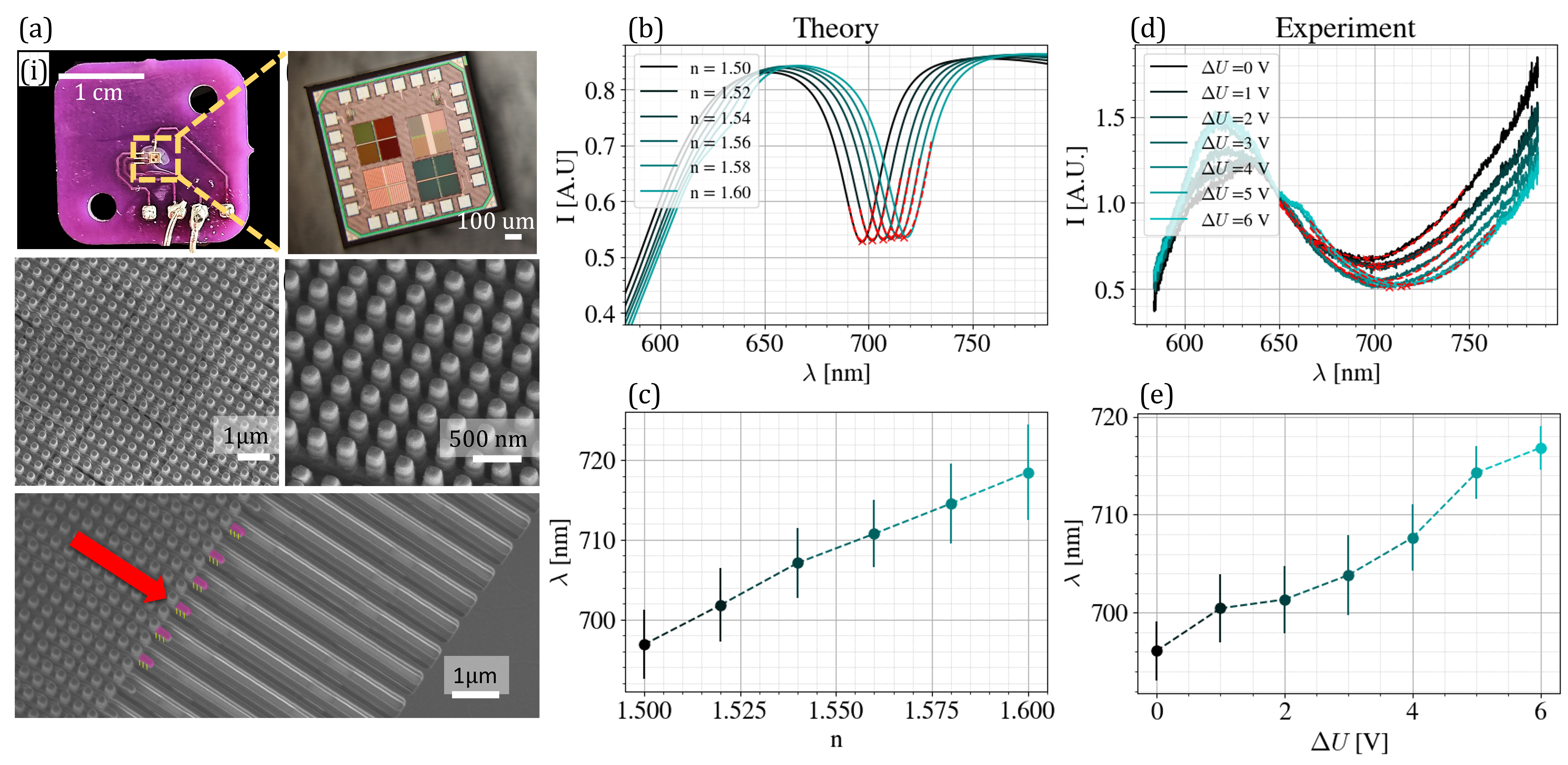
To realize an LC modulator, we drop-cast LC molecules (E7- Merck) on the device and applied a bias across the electrodes. Fig. 3(b) displays the theoretically calculated reflectance spectrum in relation to the refractive index of the superstrate. The extracted minimum reflectance wavelengths, representing the resonant wavelength, are illustrated in Fig. 3(c). The experimentally measured reflectance vs. the and the corresponding minimum reflectance wavelength are shown in Figs. 3(d) and Fig. 3(e), respectively (see supplementary materials for details on the experimental setup). The results indicate that as we increase the voltage the plasmonic resonant red-shifts, as expected from LC with positive birefringence.
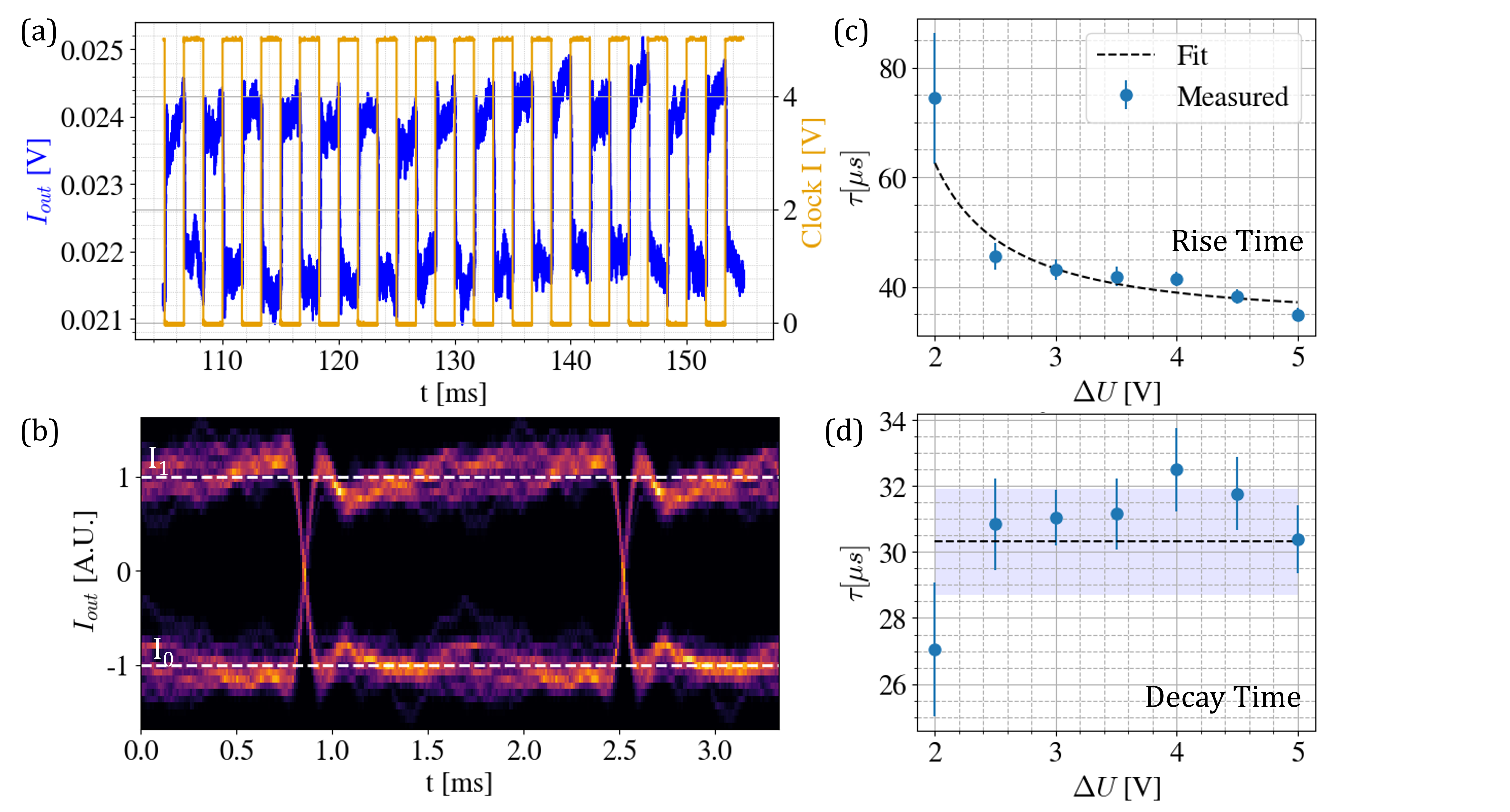
To measure the modulator response time of our modulator, we applied an AC square wave and measured the device reflectance. Fig. 4(a) and Fig. 4(b) shows the dynamics of the electro-optical response of the plasmonic LC modulator as a function of time, for different values of . The reflection switching fronts can be approximated with single exponential fits [26](see Methods), while the decay time is expected to remain consistent across varying bias. The measured rise times (decay times) obtained by fitting the reflection switching fronts are shown in Fig. 4(c) (Fig. 4(d)). The values reported are the average of multiple fits from the captured time series at Hz. The error bars represent the standard error of the mean obtained from the multiple fits and we confirmed these results by measuring the 20-80 rise time shown in Fig. 7, which supports the fit results (see Methods and appendixes). For the decay time, a weighted average was computed and is illustrated in Fig. 4(d) in a black dashed line, with the standard deviation from the mean depicted in blue. The average decay time is 30.4 2.1 s. For rise times, at , the measured rise time is = 27.49 3.33 which corresponds to a modulation speed KHz, which is two orders of magnitude faster than state-of-the-art LC modulators.
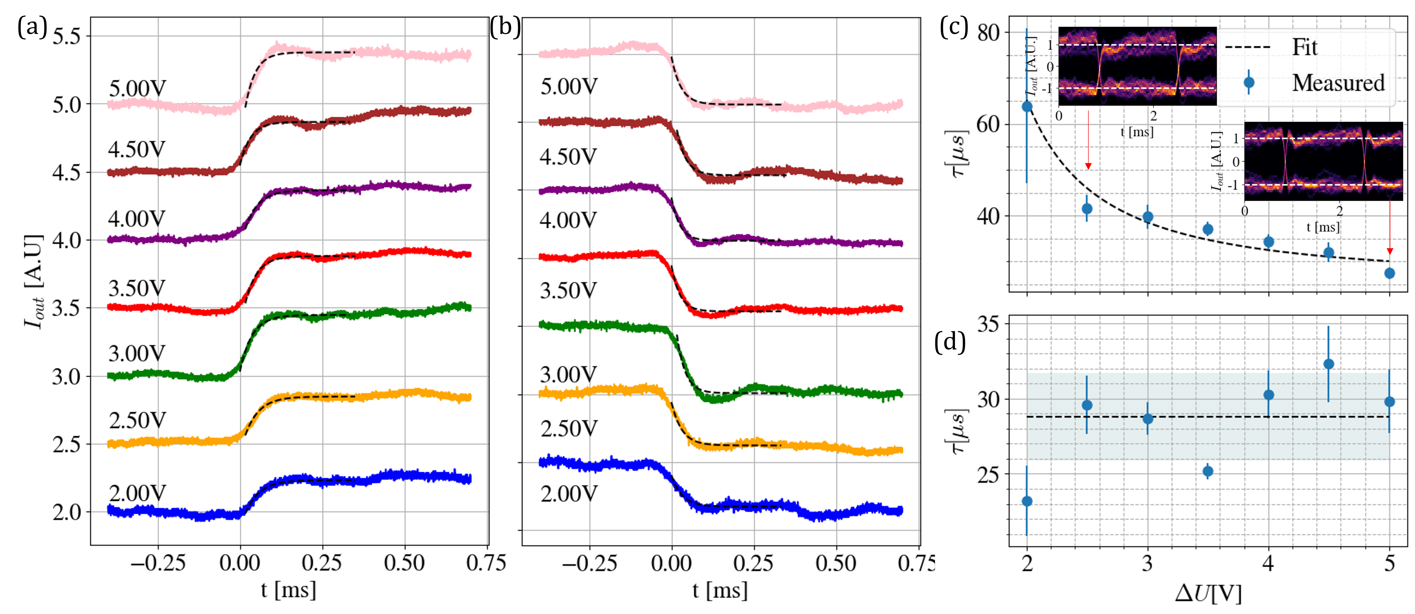
The rise time vs. voltage results are then fitted with equation 1 to extract the effective cell size and the value of at infinite potential difference in Fig. 4(b). For typical parameters of E7 liquid crystals ( viscosity coefficient , elastic constant and ), the calculated is 55.5 6.9 nm and the free parameter is . We found that the fitted value of the cell size is smaller than the numerically predicted effective cell thickness, which is likely due to the immobilized liquid crystal molecules near each interface, reducing the effective cell size. A similar calculation can be performed for the decay time, see Appendix C.
5 Conclusions and Future Outlook
We have introduced a fabless model that enables the fabrication of metal-optic devices and the co-integration of photonics and electronics in bulk CMOS foundry processes. Using a 65-nm CMOS process, we fabricated arrays of metallic nanorods, which are among the most important building blocks in metal-optics due to their strong optical nonlinearities and high refractive index sensitivity [32, 33, 34, 35]. We expect that future works will develop plasmonic nano-rod-based devices in CMOS foundries and directly integrate them with CMOS electronic devices.
With minimal post-processing, we integrated liquid crystals into the nano-rod array and demonstrated an LC optical modulator with speeds two orders of magnitude faster than those of state-of-the-art LC modulators. This work serves as a foundation for fabricating electro-optic devices in CMOS foundries, including the creation of LiDARs and spatial light modulators. Other electro-optic materials with higher response speeds, such as electro-optic polymers, can also be integrated into these devices.
The fabless nanophotonic model has the potential to spur growth in the metal-optic research and industry, similar to the impact of the fabless model on silicon photonics. Due to fabrication difficulties, many metal-optic devices were demonstrated at microwave frequencies [36, 37]. Moreover, metal-optic devices that require multilayer fabrication with precise alignment can be easily demonstrated using the proposed metal-optics fabless model [38, 39]. The possibility of integrating metal-optic devices with other electronic components commonly fabricated in CMOS foundries—such as electromagnets, heaters, transistors, and CMOS photodetectors—will pave the way for a new generation of nanophotonic devices.
6 Methods
6.1 Removing the CMOS passivation layer
In CMOS chips a passivation layer protects the underlying semiconductor devices and circuitry from damage and degradation. We removed this passivation layer to integrate LC molecules with deep metal layers in the CMOS stack.
The passivation layer is typically made of dielectric materials with good insulating and chemical barrier properties. Common materials used for passivation layers include silicon dioxide (), silicon nitride (), and silicon oxynitride (SiON). We used reactive ion etching (RIE) , (Plasma-Therm) to remove these layers. The etching was done using Carbon Tetrafluoride () gas. Note that the Cu nanostructures act as a hard mask during the RIE process. This means that right below the Cu structure, a dielectric layer is present. The exact nature and optical properties of the dielectric layer was not supplied by the manufacturer. The etching rate was nm/min and took a total of 3 hours using W and mTorr. The etching process was done in steps of 15 minutes to allow for the sample to cool down and to avoid overheating of the substrate, which would collapse the nanostructures. We found that these conditions vary significantly depending on the tool used.
6.2 FDTD calculations
All numerical simulations were carried out using the finite difference time domain (FDTD) method (Lumerical™). When designing our plasmonic devices, we used the perfectly matched layer (PML) boundary condition in direction and the periodic boundary conditions in the and directions. The optical constants of Cu were taken from Palik. The ordinary and extraordinary refractive indices of the liquid crystal molecules (E7-Merck) are 1.55 and 1.75, respectively. The unetched dielectric is assumed to be silica with a refractive index = 1.45.
6.3 CMOS Layout
Following the FDTD modulator design stage, the modulator designs were imported into Cadence Virtuoso. Here, we confirmed that they followed design rules for the 65 nm process and added connections to underlying metal layers for the interdigitated electrodes. Different designs were combined onto a single die, and the electrodes were routed to wirebond pads for testing.
6.4 Reflection measurements
For our reflection measurements we mounted the sample on a microscope with a broadband source (lamp) and coupled the reflected light to a multimode fiber connected to a Thorlabs spectrometer (CCS200). Since the resonance is very broad, it is sufficient to fit it with a quadratic polynomial in order to estimate the resonant wavelength. We fit a quadratic polynomial around the dip:
| (2) |
Where and are fitting parameters. The resonant wavelength is the minimal value:
| (3) |
We extract the error for the value from the square root of the covariance matrix of the fit, which gives errors on the fit parameters, and calculate the error for :
| (4) |
The same procedure was applied for measuring the resonant wavelength of the simulated spectra.
6.5 Response time measurements
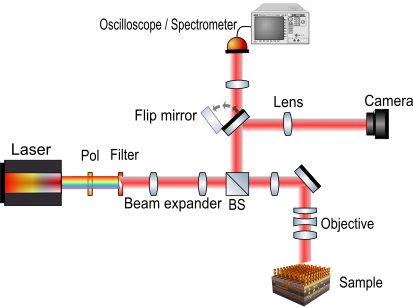
We built an optical microscopy setup (Fig. 5) to measure the response time of our devices. We used a broadband supercontinuum source (SuperK EXTREME Super-continuum Lasers - EXW-12 from NKT Photonics). The source is filtered with a 690 nm filter with a FWHM of 10 nm and the beam is expanded and collimated on our sample using a 50X Mitutoyo IR objective. The reflected light is imaged onto a visible camera (Thorlabs Zelux® 1.6 MP Color CMOS camera) as well as directed to a photo-detector (Thorlabs APD430C) that connects to an oscilloscope/spectrometer. All rise time measurements were performed on this optical setup. Time series measurements were acquired from the APD output on an oscilloscope. We used a signal generator to produce a square wave at 300 Hz applied to the sample and applied a high-pass filter on the measured data to remove slow drifting of the entire field. For each clock period the measured intensity was fitted to an exponential:
| (5) |
Where is the measured intensity of the instance, is the amplitude of the fit, is time, is the zero time, is a constant shift and is the rise time. The final value was calculated according to the central limit theorem:
| (6) |
Where is the mean value, is the fit of the instance, is the number of instances and is the standard deviation.
6.6 Effective Cell Thickness Calculation
We calculated for each voltage from 2 V to 5 V and fit the data (weighted least squares) to:
| (7) |
where is the minimum value of in the limit of , is the voltage, is the threshold voltage for E7 LC and is taken to be 1.3 V [26], and = , where and are the viscosity coefficient and the elastic constant of the LC, respectively, and is the LC cell thickness. The effective cell thickness can then be extracted from the fit:
| (8) |
Where is the error fir the fit parameter b. For the decay time, the same equation can be used, .
6.7 LC dynamics simulations
We used SHINTECH OPTICS LCDMaster 3D software to model the LC dynamics. The software allows the user to simulate complex 3D rotation of liquid crystals. Fig. 1 and Fig. 2(d) in the manuscript show the orientation of LC molecules calculated using the LCDMaster software with a bias OFF and ON, respectively. The dimensions for the device are the same as the one used in FDTD simulations and obtained from TSMC. The unit cell has a height of and base dimensions of 2 and (where is the pitch). To simulate the liquid crystal dynamics for an infinite 2D array of nanorods, we treat the unit cell with periodic boundary conditions in the and directions. The minimum distance between meshes was taken to be . The temporal resolution used to simulate dynamics was 0.08 , and the simulation length was set to be 1 ms. A step voltage is applied across the nanorod electrodes at the start of the simulation (i.e. we set the adjacent nanorods to have voltages of and ).
The initial alignment director has a pre-tilt of 2 degrees on floor and ceiling. The anchoring conditions were set to zero anchoring on the ceiling (since we drop cast the LCs and the interface is with air) and weak anchoring on the floor. The simulation parameters used were: , , [40], and [41]. After running the simulation, at each timestep we calculated the angular deviation , defined as:
| (9) |
where and are the azimuthal and polar angles of the LC at time as defined in Fig. 8(a). The angular deviation was integrated over a volume , corresponding to the region where the field is large (according to FDTD simulations):
| (10) |
Acknowledgments We thank the MITRE Quantum Moonshot Program for program oversight and funding. Experiments were supported in part by Army Research Office grant W911NF-20-1-0084. We thank the MIT.nano staff for fabrication assistance. S.T.M. was supported by the Schmidt Postdoctoral Award and the Israeli Vatat Scholarship. C.B. is supported by NSF GRFP. H.Z.Y. and A.W. were supported by MIT UROP program. I.H. is supported by the STC Center for Integrated Quantum Materials (CIQM) NSF Grant No. DMR-1231319, the National Science Foundation (NSF) Engineering Research Center for Quantum Networks (CQN) awarded under cooperative agreement number 1941583, and the MITRE Moonshot Program.
Authors’ contributions D.E., R.H., and M.E. conceived the idea. M.E. and S.T.M. led the research and performed the experiments, built the experimental setups and performed the data analysis. M.E. developed the post fabrication procedure, designed the plasmonic device and liquid crystal modulator, and performed the FDTD simulations. I.H., M.I., and X.C performed the CMOS tapeout. S.B. designed the printed circuit board (PCB). S.B. and H.Y. helped with the rise time experiments. C.B. contributed to the data analysis. A.W. performed the liquid crystal simulations. D.E. and R.H. supervised the research. M.E., S.T.M. and D.E. wrote the manuscript with input from all authors.
Appendix A Optical Setup
Illustrated in Fig. 5 is a schematic representation of the optical configuration employed in our experimental setup. The broad-spectrum source is polarized and is subsequently filtered through a 690 nm bandpass filter. It is then collimated onto the sample utilizing a 4- system comprising a focusing lens and an objective (Mitutoyo NIR objective). The reflected light can be directed towards a fiber coupled photodetector (Thorlabs APD430), connected to a spectrometer or oscilloscope, or a camera through the use of a flip mirror. The sample is affixed to a printed circuit board (PCB) and is subject to controlled adjustments for tip/tilt. The same setup was used for measuring the rise time and decay time.
Appendix B Passivation Layer Removal
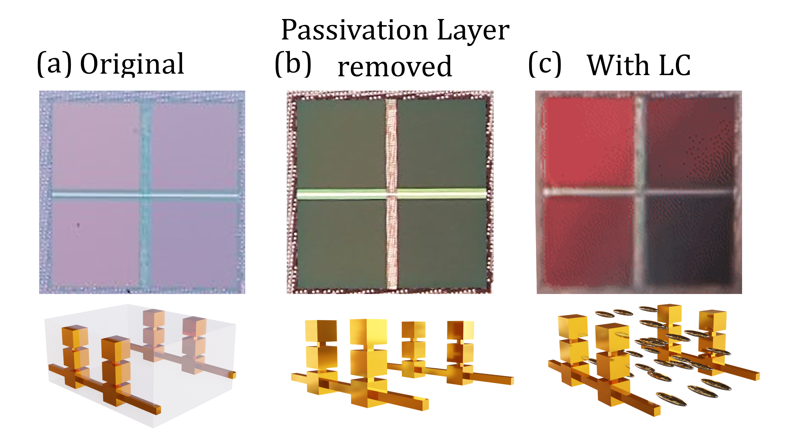
During the post-processing stage involving the removal of the passivation layer through ion etching, a change in pixel color becomes apparent throughout the procedure. The pixels retaining the passivation layer exhibit a diffused red hue. As depicted in Fig. 6, alterations in pixel color are observed subsequent to the removal of the passivation layer and the introduction of LCs. Specifically, the transition ensues from a diffused red tone to green, eventually reverting to a vivid red with the incorporation of LCs. The change in color confirms that the nano-rods support a plasmonic resonance that is sensitive to variations in the local refractive index.
Appendix C 20-80 Rise time analysis.
In addition to fitting an exponent to retrieve the rise time, we performed a 20-80 rise time analysis. We constructed an eye diagram from a time-series measurement at 300 Hz for every applied , as can be seen in Fig. 7(b). The and values were calculated as the average value of all the data samples captured inside the middle 20% (40% to 60% points) of the eye period. The 20-80 rise time was calculated as the time difference between the last cross of the data with 20% of the total height, , and the first cross of the data with 80% of the total height .
| (11) |
For the decay time of the modulator , the analysis was based on equation 12, with a modification: the 20-80 decay time is defined as the time difference between the last instance when the data crosses 80 % of the total height and the first instance when it crosses 20 %:
| (12) |
In both cases, We used equation 6 to calculate the rise time and error for every . The relation between (both for rise time and decay time) and is given by:
| (13) |
Fig. 7(c) shows a fit to equation 7. The effective cell thickness was calculated according to equation 8. The fitted value is = 47.2 6.5 nm and = 34.9 3.1 . These values are within the error of values reported in the main text. The minimal measured value = 28.18 2.16 at = 5 V.
Our expectation is that the decay time remains consistent across varying bias. A weighted average of the decay times was computed and is illustrated in Fig. 7(d). The average decay time obtained from the 20-80 analysis is 30.7 1.5 s. This value is well within the standard deviation of the value reported from the exponential fit analysis.
We can derive the effective cell thickness for the decay time from equation 8. This calculation yields = 41.9 1.5 nm and = 42.1 1.0 nm for the exponential fitting and 20-80 analysis respectively. The effective cell thickness calculated from the measured decay time and measured rise time are within the error of both, which suggests that the two measurements are statistically consistent within the uncertainties of each method.
Appendix D Simulated LC dynamics.
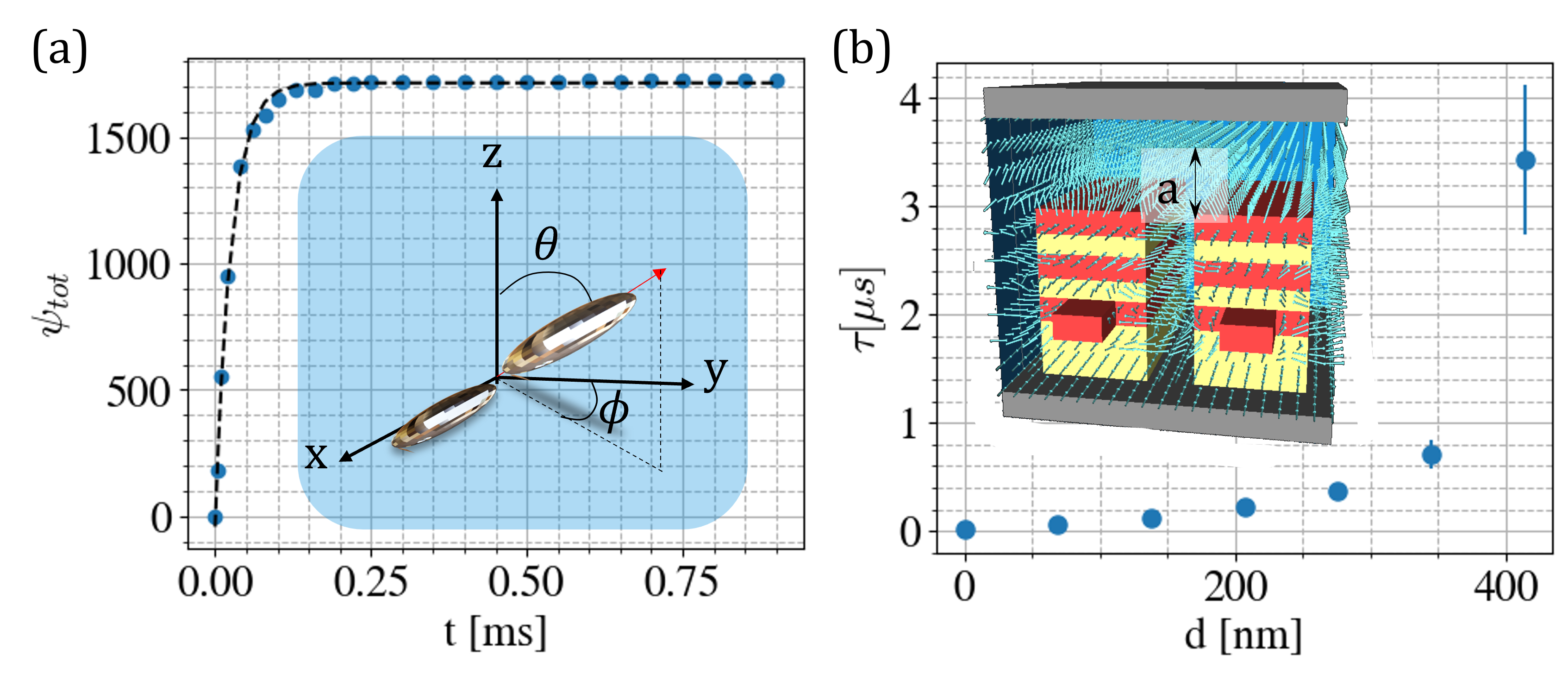
To evaluate the rotational dynamics of LC molecules, we conducted simulations using Shintech LCDMaster3D. Fig. 8(a) shows the simulated integrated angular deviation over the simulation time, and the exponential fit used to extract the rise time. The angular deviation was integrated over the area between the rods, where the electric field attains a high magnitude, as obtained from the COMSOL simulations, and can be seen in Fig. 2(c).
Additionally, we explored how this rise time varies with respect to the vertical distance from the nanorods, denoted as and defined in Fig. 8(a)(inset). Our findings indicate an exponential increase in the LC rotation time with increasing distance from the nano-rods. Fig. 8(b) shows the rise time as a function of , where this exponential relation is evident. The rise time at = 414 nm above the nanorods is 3.4 0.6 ms, surpassing the value at = 0 nm by more than 200-fold.
References
- \bibcommenthead
- Haffner et al. [2018] Haffner, C., Chelladurai, D., Fedoryshyn, Y., Josten, A., Baeuerle, B., Heni, W., Watanabe, T., Cui, T., Cheng, B., Saha, S., Elder, L.R. Delwin L. Dalton, Boltasseva, A., Shalaev, V.M., Kinsey, N., JLeuthold, u.: Low-loss plasmon-assisted electro-optic modulator. Nature 556(7702), 483–486 (2018)
- ElKabbash et al. [2019] ElKabbash, M., Sreekanth, K.V., Alapan, Y., Kim, M., Cole, J., Fraiwan, A., Letsou, T., Li, Y., Guo, C., Sankaran, R.M., Gurkan, U.A., Hinczewski, M., Strangi, G.: Hydrogen sensing using thin-film perfect light absorber. ACS Photonics 6(8), 1889–1894 (2019)
- Pors et al. [2015] Pors, A., Nielsen, M.G., Bozhevolnyi, S.I.: Analog computing using reflective plasmonic metasurfaces. Nano letters 15(1), 791–797 (2015)
- Zangeneh-Nejad et al. [2021] Zangeneh-Nejad, F., Sounas, D.L., Alù, A., Fleury, R.: Analogue computing with metamaterials. Nature Reviews Materials 6(3), 207–225 (2021)
- Madsen et al. [2022] Madsen, L.S., Laudenbach, F., Askarani, M.F., Rortais, F., Vincent, T., Bulmer, J.F., Miatto, F.M., Neuhaus, L., Helt, L.G., Collins, M.J., Lita, A.E., Gerrits, T., Nam, S.W., Vaidya, V.D., Menotti, M., Dhand, I., Vernon, Z., Quesada, N., Lavoie, J.: Quantum computational advantage with a programmable photonic processor. Nature 606(7912), 75–81 (2022)
- ElKabbash et al. [2021] ElKabbash, M., Letsou, T., Jalil, S.A., Hoffman, N., Zhang, J., Rutledge, J., Lininger, A.R., Fann, C.-H., Hinczewski, M., Strangi, G., Guo, C.: Fano-resonant ultrathin film optical coatings. Nature Nanotechnology 16(4), 440–446 (2021)
- Lee et al. [2023] Lee, K.J., Wei, R., Wang, Y., Zhang, J., Kong, W., Chamoli, S.K., Huang, T., Yu, W., ElKabbash, M., Guo, C.: Gigantic suppression of recombination rate in 3d lead-halide perovskites for enhanced photodetector performance. Nature Photonics, 1–8 (2023)
- ElKabbash [2022] ElKabbash, M.: Radiative cooling with angular shields: Mitigating atmospheric radiation and parasitic heating. arXiv preprint arXiv:2208.03797 (2022)
- Bandyopadhyay et al. [2022] Bandyopadhyay, S., Sludds, A., Krastanov, S., Hamerly, R., Harris, N., Bunandar, D., Streshinsky, M., Hochberg, M., Englund, D.: Single chip photonic deep neural network with accelerated training. arXiv preprint arXiv:2208.01623 (2022)
- Menssen et al. [2022] Menssen, A.J., Hermans, A., Christen, I., Propson, T., Li, C., Leenheer, A.J., Zimmermann, M., Dong, M., Larocque, H., Raniwala, H., Gilbert, G., Eichenfield, M., Englund, D.R.: Scalable photonic integrated circuits for programmable control of atomic systems. arXiv preprint arXiv:2210.03100 (2022)
- Christen et al. [2022] Christen, I., Sutula, M., Propson, T., Sattari, H., Choong, G., Panuski, C., Melville, A., Mallek, J., Hamilton, S., Dixon, P.B., Menssen, A.J., Braje, D., Ghadimi, A.H., Englund, D.R.: An integrated photonic engine for programmable atomic control. arXiv preprint arXiv:2208.06732 (2022)
- Hochberg and Baehr-Jones [2010] Hochberg, M., Baehr-Jones, T.: Towards fabless silicon photonics. Nature photonics 4(8), 492–494 (2010)
- Shainline et al. [2013] Shainline, J.M., Orcutt, J.S., Wade, M.T., Nammari, K., Moss, B., Georgas, M., Sun, C., Ram, R.J., Stojanović, V., Popović, M.A.: Depletion-mode carrier-plasma optical modulator in zero-change advanced cmos. Optics letters 38(15), 2657–2659 (2013)
- Alloatti et al. [2016] Alloatti, L., Cheian, D., Ram, R.J.: High-speed modulator with interleaved junctions in zero-change cmos photonics. Applied Physics Letters 108(13), 131101 (2016)
- Alloatti et al. [2015] Alloatti, L., Srinivasan, S., Orcutt, J.S., Ram, R.J.: Waveguide-coupled detector in zero-change complementary metal–oxide–semiconductor. Applied Physics Letters 107(4), 041104 (2015)
- Orcutt et al. [2011] Orcutt, J.S., Khilo, A., Holzwarth, C.W., Popović, M.A., Li, H., Sun, J., Bonifield, T., Hollingsworth, R., Kärtner, F.X., Smith, H.I., Stojanović, V., J. Ram, R.: Nanophotonic integration in state-of-the-art cmos foundries. Optics express 19(3), 2335–2346 (2011)
- Atabaki et al. [2018] Atabaki, A.H., Moazeni, S., Pavanello, F., Gevorgyan, H., Notaros, J., Alloatti, L., Wade, M.T., Sun, C., Kruger, S.A., Meng, H., Al Qubaisi, K., Wang, I., Zhang, B., Khilo, A., Baiocco, C.V., Popović, M.A., Stojanović, V.M., Ram, R.J.: Integrating photonics with silicon nanoelectronics for the next generation of systems on a chip. Nature 556(7701), 349–354 (2018)
- Yesilkoy et al. [2019] Yesilkoy, F., Arvelo, E.R., Jahani, Y., Liu, M., Tittl, A., Cevher, V., Kivshar, Y., Altug, H.: Ultrasensitive hyperspectral imaging and biodetection enabled by dielectric metasurfaces. Nature Photonics 13(6), 390–396 (2019)
- Miller [2017] Miller, D.A.: Attojoule optoelectronics for low-energy information processing and communications. Journal of Lightwave Technology 35(3), 346–396 (2017)
- Zou et al. [2021] Zou, J., Yang, Q., Hsiang, E.-L., Ooishi, H., Yang, Z., Yoshidaya, K., Wu, S.-T.: Fast-response liquid crystal for spatial light modulator and lidar applications. Crystals 11(2), 93 (2021)
- Chen et al. [2019] Chen, R., Huang, Y., Li, J., Hu, M., Li, J., Chen, X., Chen, P., Wu, S.-T., An, Z.: High-frame-rate liquid crystal phase modulator for augmented reality displays. Liquid Crystals 46(2), 309–315 (2019)
- Molesky et al. [2018] Molesky, S., Lin, Z., Piggott, A.Y., Jin, W., Vucković, J., Rodriguez, A.W.: Inverse design in nanophotonics. Nature Photonics 12(11), 659–670 (2018)
- Mkhitaryan et al. [2021] Mkhitaryan, V., March, K., Tseng, E.N., Li, X., Scarabelli, L., Liz-Marzán, L.M., Chen, S.-Y., Tizei, L.H., Stéphan, O., Song, J.-M., Kociak, M., Abajo, F.J., Gloter, A.: Can copper nanostructures sustain high-quality plasmons? Nano Letters 21(6), 2444–2452 (2021)
- Gérard and Gray [2014] Gérard, D., Gray, S.K.: Aluminium plasmonics. Journal of Physics D: Applied Physics 48(18), 184001 (2014)
- Si et al. [2014] Si, G., Zhao, Y., Leong, E.S.P., Liu, Y.J.: Liquid-crystal-enabled active plasmonics: a review. Materials 7(2), 1296–1317 (2014)
- Gorkunov et al. [2017] Gorkunov, M., Kasyanova, I., Artemov, V., Barnik, M., Geivandov, A., Palto, S.: Fast surface-plasmon-mediated electro-optics of a liquid crystal on a metal grating. Physical Review Applied 8(5), 054051 (2017)
- Gigan et al. [2022] Gigan, S., Katz, O., De Aguiar, H.B., Andresen, E.R., Aubry, A., Bertolotti, J., Bossy, E., Bouchet, D., Brake, J., Brasselet, S., Bromberg, Y., Cao, H., Chaigne, T., Cheng, Z., Choi, W., Čižmár, T., Cui, M., R Curtis, V., Defienne, H., Hofer, M., Horisaki, R., Horstmeyer, R., Ji, N., LaViolette, A.K., Mertz, J., Moser, C., Mosk, A.P., Pégard, N.C., Piestun, R., Popoff, S., Phillips, D.B., Psaltis, D., Rahmani, B., Rigneault, H., Rotter, S., Tian, L., Vellekoop, L. Ivo M nad Waller, Wang, L., Weber, T., Xiao, S., Xu, C., Yamilov, A., Yang, C., Yılmaz, H.: Roadmap on wavefront shaping and deep imaging in complex media. Journal of Physics: Photonics 4(4), 042501 (2022)
- Lucente [2011] Lucente, M.: The first 20 years of holographic video—and the next 20. In: SMPTE 2nd Annual International Conference on Stereoscopic 3D for Media and Entertainment, pp. 21–23 (2011)
- Agnew et al. [2011] Agnew, M., Leach, J., McLaren, M., Roux, F.S., Boyd, R.W.: Tomography of the quantum state of photons entangled in high dimensions. Physical Review A 84(6), 062101 (2011)
- Li et al. [2019] Li, S.-Q., Xu, X., Maruthiyodan Veetil, R., Valuckas, V., Paniagua-Domínguez, R., Kuznetsov, A.I.: Phase-only transmissive spatial light modulator based on tunable dielectric metasurface. Science 364(6445), 1087–1090 (2019)
- Lyvers et al. [2008] Lyvers, D.P., Moon, J.-M., Kildishev, A.V., Shalaev, V.M., Wei, A.: Gold nanorod arrays as plasmonic cavity resonators. ACS nano 2(12), 2569–2576 (2008)
- Wang et al. [2018] Wang, P., Krasavin, A.V., Nasir, M.E., Dickson, W., Zayats, A.V.: Reactive tunnel junctions in electrically driven plasmonic nanorod metamaterials. Nature nanotechnology 13(2), 159–164 (2018)
- Kabashin et al. [2009] Kabashin, A.V., Evans, P., Pastkovsky, S., Hendren, W., Wurtz, G.A., Atkinson, R., Pollard, R., Podolskiy, V.A., Zayats, A.V.: Plasmonic nanorod metamaterials for biosensing. Nature materials 8(11), 867–871 (2009)
- Vestler et al. [2018] Vestler, D., Shishkin, I., Gurvitz, E., Nasir, M., Ben-Moshe, A., Slobozhanyuk, A., Krasavin, A.V., Levi-Belenkova, T., Shalin, A., Ginzburg, P., Markovich, G., Zayats, A.V.: Circular dichroism enhancement in plasmonic nanorod metamaterials. Optics express 26(14), 17841–17848 (2018)
- Wurtz et al. [2011] Wurtz, G.A., Pollard, R., Hendren, W., Wiederrecht, G., Gosztola, D., Podolskiy, V., Zayats, A.V.: Designed ultrafast optical nonlinearity in a plasmonic nanorod metamaterial enhanced by nonlocality. Nature nanotechnology 6(2), 107–111 (2011)
- Camacho et al. [2021] Camacho, M., Edwards, B., Engheta, N.: A single inverse-designed photonic structure that performs parallel computing. Nature Communications 12(1), 1466 (2021)
- Silva et al. [2014] Silva, A., Monticone, F., Castaldi, G., Galdi, V., Alù, A., Engheta, N.: Performing mathematical operations with metamaterials. Science 343(6167), 160–163 (2014)
- Park et al. [2020] Park, J.-H., Ndao, A., Cai, W., Hsu, L., Kodigala, A., Lepetit, T., Lo, Y.-H., Kanté, B.: Symmetry-breaking-induced plasmonic exceptional points and nanoscale sensing. Nature Physics 16(4), 462–468 (2020)
- Liu et al. [2009] Liu, N., Langguth, L., Weiss, T., Kästel, J., Fleischhauer, M., Pfau, T., Giessen, H.: Plasmonic analogue of electromagnetically induced transparency at the drude damping limit. Nature materials 8(9), 758–762 (2009)
- Jacobs et al. [1992] Jacobs, S.D., Marshall, K., Schmid, A., OPTICS, R.U.N.I.O.: Liquid Crystals for Laser Applications. Laboratory for Laser Energetics, College of Engineering and Applied Science …, ??? (1992)
- Gorkunov et al. [2017] Gorkunov, M., Kasyanova, I., Artemov, V., Barnik, M., Geivandov, A., Palto, S.: Fast surface-plasmon-mediated electro-optics of a liquid crystal on a metal grating. Physical Review Applied 8(5), 054051 (2017)