Modeling of Surface Damage at the Si/SiO2-interface of Irradiated MOS-capacitors
Abstract
Surface damage caused by ionizing radiation in SiO2 passivated silicon particle detectors consists mainly of the accumulation of a positively charged layer along with trapped-oxide-charge and interface traps inside the oxide and close to the Si/SiO2-interface. High density positive interface net charge can be detrimental to the operation of a multi-channel -on- sensor since the inversion layer generated under the Si/SiO2-interface can cause loss of position resolution by creating a conduction channel between the electrodes. In the investigation of the radiation-induced accumulation of oxide charge and interface traps, a capacitance-voltage characterization study of n/- and -irradiated Metal-Oxide-Semiconductor (MOS) capacitors showed that close agreement between measurement and simulation were possible when oxide charge density was complemented by both acceptor- and donor-type deep interface traps with densities comparable to the oxide charges. Corresponding inter-strip resistance simulations of a -on- sensor with the tuned oxide charge density and interface traps show close agreement with experimental results. The beneficial impact of radiation-induced accumulation of deep interface traps on inter-electrode isolation may be considered in the optimization of the processing parameters of isolation implants on -on- sensors for the extreme radiation environments.
1 Introduction
In the high-radiation environment of LHC experiments, where silicon particle detectors are utilized, radiation-induced defects are introduced both in the silicon substrate (bulk damage or displacement damage) and in the SiO2 passivation layer, that affect the sensor performance through the interface with the Si-bulk (surface damage). An accompanying study to the investigation presented here focused on the influence of displacement damage on the bulk properties of test-diode samples exposed to a reactor radiation environment [1]. In this study, the influence and accumulation of surface damage is investigated by the characterizations of Metal-Oxide-Semiconductor (MOS) capacitors, exposed to either the same reactor radiation environment as in the previous study or to a -source.
Surface damage caused by ionizing radiation from charged particles, X-rays or gammas in SiO2 passivated devices consists of the accumulation of positively charged layer (fixed oxide charge density that does not move or exchange charge with Si), trapped-oxide-charge and interface traps (or surface states ), along with mobile-ionic-charge density () inside the oxide and close to the interface with silicon bulk. When exposed to high-energy ionizing radiation, electron-hole pairs are created in the oxide. The fraction of electrons and holes escaping from the initial recombination drift through the oxide either to the gate-electrode or to the Si/SiO2-interface, depending on the gate bias. Holes transport with positive gate bias through the oxide toward the Si/SiO2-interface by hopping through localized states in the oxide, and a fraction of the holes that reach the vicinity of the interface are captured by oxygen vacancies (most of the vacancies in the SiO2 are located close to the Si/SiO2-interface) and form positive oxide-trapped charge. During the transport of holes, some react with hydrogenated oxygen vacancies and result in protons (hydrogen ions). The fraction of protons that drift to the interface produce dangling Si-bonds, i.e. interface traps, by breaking the hydrogenated Si-bonds at the interface. The mechanisms by which surface damage accumulation occurs are described extensively in [2, 3, 4, 5, 6].
High positive is detrimental to the functionality of segmented -on- (-bulk with electrode implants) sensors, since the electron layer generated under the Si/SiO2-interface can cause loss of position resolution by providing a conduction channel that compromises the inter-electrode isolation. Additionally, the accumulating interface charges can contribute to higher channel noise by the increase of inter-electrode capacitance () and modify the electric fields at the edges of the isolation- and channel-implants. can also play a notable role in determining the surface properties of Si-sensors as significant fraction of these interface states have been reported to be deep traps with densities comparable to [7, 8] in X-ray irradiated devices, thus capable of altering the space charge near the Si/SiO2-interface.
Device simulations play a vital role in understanding and parametrizing the observed macroscopic effects of the microscopic surface states and charges at the Si/SiO2-interface. Previous simulation studies to model the radiation-induced accumulation of surface damage involve several approaches, of which one is to approximate the surface damage solely by (for the modeling of inter-strip resistance () in Ref. [9], in Ref. [10] and electric field surface distribution in Ref. [11]). Models complementing with interface traps include approaches presented in Table1.
| type | [eV] | Tuning properties | Reference |
|---|---|---|---|
| Deep acceptor | and | [12] | |
| Shallow acceptor | |||
| Deep donor | and | [13, 14] | |
| Deep acceptor | |||
| Deep donor | [15] | ||
| Deep acceptor | |||
| Shallow acceptor |
A further model, tuned to reproduce the charge-injection position dependence of charge collection efficiency (CCE()) in the inter-strip region and , includes an approach where two bulk defect levels tuned for proton irradiation [16] are augmented by a shallow ( eV) with 2 m depth distribution from the surface [17, 18].
It needs to be pointed out that for higher tunability of the models the use of a single set of effective interface traps is an approximation of the real situation, where there can be a continuum of levels at the interface.
The approach taken in this study is to first tune and the parameters of (number of , type, energy level, trapping cross-sections and density) to reproduce -characteristics of irradiated MOS-capacitors and next, as a confidence level test of the tuning, monitor their possible influence on the of a -on- strip-sensor. The inter-strip isolation results are further examined for the dynamical influence of the fully occupied on the net in the operating conditions of reverse biased -on- sensors.
The paper is arranged by first introducing the samples, the neutron fluences and the -doses the samples were exposed to in Section 2. Next, the measurement and simulation setups are descibed in Section 3. -characterization results start with the analysis of pre-irradiated reference MOS-capacitors diced from 6-inch wafers in Section 4.1, where the extracted oxide thicknesses () and oxide charge densities at the Si/SiO2-interface () are presented. Results of both reactor neutron and -irradiated MOS-capacitors are presented in Section 4.2 by first determining the change in the flat band voltage () after irradiation, followed by the extraction of effective oxide charge density () at the Si/SiO2-interface. Technology Computer-Aided Design (TCAD) simulations are applied in both results sections to reproduce and model the measured -characteristics. The inter-strip resistance simulations applying and surface states tuned to reproduce the irradiated MOS-capacitor -characteristics are presented in the second part of Section 4.2. Finally, the results are discussed in Section 5, while summary and conclusions are given in Section 6.
2 Samples, effective neutron fluences and doses
Out of five reactor irradiated samples in this study, three were irradiated at Rhode Island Nuclear Science Center111http://www.rinsc.ri.gov/ (RINSC) and two at UC Davis McClellan Nuclear Research Center222https://mnrc.ucdavis.edu/ (MNRC). Total Ionizing Dose (TID) in both reactor cores was from a mixed field of neutrons and gammas, while the contribution from gammas was expected to dominate TID. Monte Carlo N-Particle Transport (MCNP) simulations indicated that neutron contribution to TID was only about 5% at MNRC. In addition, three samples were -irradiated at Sandia National Laboratories Gamma Irradiation Facility333https://www.sandia.gov/research/gamma-irradiation-facility-and-low-dose-rate-irradiation-facility/ (GIF) with a 60Co-source. After irradiations, the samples were shipped cooled in thermally isolated containers to Texas Tech University (TTU) to avoid annealing of the radiation-induced defects and were then stored at - C between the measurements.
Samples like one shown in Figure 1 were diced from 6-inch Hamamatsu Photonics K.K. (HPK) sensor-wafers with crystal orientation. The test structures on the samples were designed at Institut für Hochenergiephysik (HEPHY). Two distinct diffusion processes were applied in the samples with MOS-capacitors to produce the heavily-doped backplane blocking contact: standard-diffusion (‘std-FZ’) to produce 300- active thickness sensors and deep-diffusion (‘dd-FZ’) for 200- and 120- active thicknesses, while the physical thickness of all samples was 320 . Sample identification of e.g. ‘300P-std-FZ’ in Table 2, refers to a 300--active thickness MOS-capacitor with -type float-zone Si-bulk and standard-diffused backplane implant. Gate oxide in all samples was silicon dioxide (SiO2) with positive oxide charge. The corresponding effective 1-MeV neutron equivalent fluences () extracted from the test-diode leakage currernts in the samples, -doses and MCNP-simulated TIDs are also presented in Table 2. Details of the effective fluence extraction and the bulk properties of the samples are given in [1].

| Sample ID, | Irradiation | D | MCNP TID | |
| thickness & type | site | [cm] | [kGy] | [kGy] |
| N1(n): 300N-std-FZ | RINSC | – | – | |
| N2(n): 300N-std-FZ | MNRC | – | ||
| N3(n): 120N-dd-FZ | RINSC | – | – | |
| N4(p): 120P-dd-FZ | RINSC | – | – | |
| N5(n): 120N-dd-FZ | MNRC | – | ||
| G1(n): 200N-dd-FZ | GIF | – | – | |
| G2(p): 300P-std-FZ | GIF | – | – | |
| G3(n): 300N-std-FZ | GIF | – | – |
3 Measurement and simulation setups
The capacitance-voltage () characterizations were carried out with a dark-box-enclosed custom probe station at TTU. The gate voltage of the MOS-capacitor is supplied by a Keithley 2410 SMU while the capacitance is read out by a Keysight E4980AL LCR-meter. The decoupling of the LCR-meter’s high- and low-terminals from the DC-circuit is accomplished by 1- capacitors. The remote control and data acquisition functions are carried out with LabVIEW™-based software. The MOS-capacitor is connected to the measurement circuit by a vacuum chuck from its backplane, which also provides fixed position, and by a probe needle on the segmented front surface.
Simulations were carried out using the Synopsys Sentaurus444http://www.synopsys.com finite-element TCAD software framework. The parameters extracted from -measurements of the MOS-capacitors (oxide thickness (), flat band capacitance () and voltage ()) and test diodes on the same samples (bulk doping () and backplane deep-diffusion doping profiles (see ref. [1] for details)) before irradiation, as well as their known gate area, were used as inputs to reproduce the devices as closely as possible by a 2D-simulation.
4 Experimental and simulation results
4.1 Results before irradiation
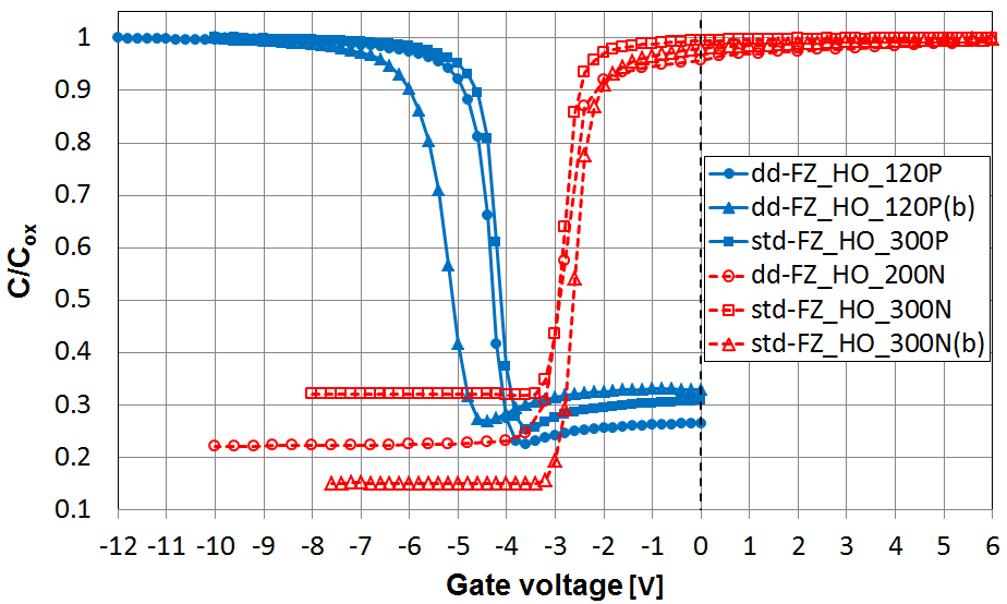
The -measurements of six reference MOS-capacitors were carried out at room temperature and the resulting -characteristics are presented in Figure 2a, where the three modes of operation –accumulation, depletion and inversion– are visible. At gate voltages with , where is the oxide capacitance, the majority carriers (holes for -bulk, electrons for -bulk) are pulled to the Si/SiO2-interface, forming an accumulation layer with zero surface potential. An abrupt drop of capacitance takes place in the depletion region, where the Si-surface is being depleted from majority carriers and measured is now and depletion layer capacitance in series. Thus, the measured keeps decreasing with gate voltage as the effective thickness of the depletion region, that acts as a dielectric between the gate and the Si-substrate, increases. Depth of the depletion region reaches its maximum, and measured its minimum (), when most of the available minority carriers are pulled to the Si/SiO2-interface (by the positive oxide charge and by the negative gate voltage for - and -bulk MOS-capacitors, respectively, in Figure 2a), forming an inversion layer. The depletion region in the measured -curve is limited by the threshold voltage (), where the surface potential equals twice the bulk potential, and the flat band voltage (), where the Si energy band becomes flat and the surface potential goes to zero [2].
Oxide thicknesses were extracted by the relation
| (1) |
where is the product of vacuum permittivity and the relative permittivity of the oxide material (SiO2), and is the MOS gate area [19]. Flat band voltages were determined by the flat-band-capacitance method with
| (2) |
where is the permittivity of the substrate material (Si) and is the extrinsic Debye length [2]. Flat band voltage is extracted from the -curve at the value of . Effective oxide charge densities at the Si/SiO2-interface were then calculated by
| (3) |
where is the metal-semiconductor work function and is the elementary charge. The results for , and of the reference MOS-capacitors are presented in Table 3. extracted from -measurements can be stated as
| (4) |
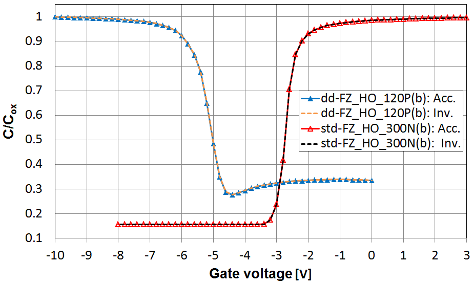
where the total value of is influenced by fixed-oxide-charge (), interface-trapped-charge () and mobile-ionic-charge () densities [2]. can be observed in -curve hysteresis when the charges (typically alkali metal ions such as Na+, K+ and Li+ before irradiation [20]) drift between metal/SiO2- and Si/SiO2-interfaces under the applied electric field, depending on the gate bias and the polarity of the charges [2, 21]. The results in Figure 2b do not show any sign of hysteresis. Scanned frequencies involved 1200 kHz, while the low mobility of in oxide (highest for Na+ with cm2/Vs at room temperature [2]) that results in long drift time from metal- to Si-interface (about 2 min with V/cm and nm), was taken into account by applying extended gate-voltage hold-time at strong inversion and strong accumulation before -sweep, respectively. Thus, the influence of in the reference samples is considered negligible, reducing Eq. 4 to . This is in contrast with previous results for thin (25 nm) SiO2 films, where significant influence of was observed [21]. The oxide films in Table 3 produced by high-growth-rate deposition method like wet thermal oxidation [22, 23] are about 30 times thicker than the oxide films in ref. [21]. Increased trapping probability of ions with substantially longer drift distance from metal- to Si-interface could explain the lack of influence from in the results.
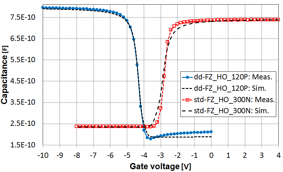
The measured -characteristics in Figure 2c were closely reproduced by TCAD simulation. Matching -values within uncertainty to the measured were reached in the simulation by using (implemented as a positive charge-sheet located at the Si/SiO2-interface with a uniform distribution along the interface) as the sole tuning parameter. Frequency-scan kHz showed no frequency dependence on the measured value of , which was repeated by the simulation. The values of (extracted from the measurement) and (required in the simulation) for 120P MOS-capacitor in Figure 2c were and , respectively, while the corresponding values for 300N were and , respectively. In four measured and simulated reference MOS-capacitors the required deviated from the measured by .
Thus, the combined hysteresis and simulation results show evidence that in the reference samples is essentially governed by , i.e. . This is in line with the results of ref. [24], where it was reported that at the Si/SiO2-interface of a non-irradiated silicon device is about two-orders-of-magnitude lower than at the interface. Therefore, the density of surface traps corresponding to should be in the order of . Additional simulation with surface-trapping-center energy of [25, 26] and a fairly large capture cross-section of results in identical -characteristics to the simulations in Figure 2c until the difference between and is less than one-order-of-magnitude.
| Sample thickness & | |||
| type | [nm] | [-V] | [] |
| 120P-dd-FZ | |||
| 120P-dd-FZ(b) | |||
| 300P-std-FZ | |||
| 200N-dd-FZ | |||
| 300N-std-FZ | |||
| 300N-std-FZ(b) |
4.2 Results after n/- and -irradiations
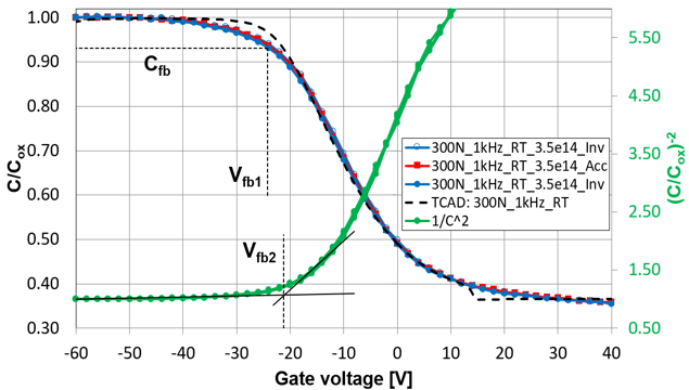
The -measurements of five n/-irradiated and three -irradiated MOS-capacitors were carried out at room temperature with frequencies 1–9 kHz, and the resulting -characteristics are presented in Figures 3–5. Due to the extended depletion-regions and the gradual change from depletion to accumulation in the -curves, most probable estimates for the of the irradiated samples were extracted by both -method in Eq. 2 and from the crossing-point of linear fits to the dynamic (depletion) and static (accumulation) regions of the reciprocal -curve, as shown in Figure 3a. The final value and the uncertainty of was then given by the average and the difference of the two extracted values, respectively. The results for and its relative change before and after irradiation () are presented in Table 4.
The change of with ionizing radiation is proportional to the change of and in Eq. 3 before ( and ) and after irradiation
| (5) |
The results of the bulk properties of the same reactor-irradiated samples in the accompanying study [1] indicate that the effective bulk doping () varies in the studied fluence range from a few times (before irradiation) to close to (at the highest fluence of about ). The dependence of leads in this range to the maximal change of , regardless of bulk polarity [2]. In comparison, the values of in Table 4 are two-orders-of-magnitude higher to . Thus, contribution from to is considered negligible in the following analysis, simplifying Eq. 5 to
| (6) |
Since the absolute values of in the n/-irradiated MOS-capacitors were observed to fluctuate significantly from the initial before irradiation, the relation applied to extract was reached by combining Eqs. 1 and 6:
| (7) |
where is solely dependent on oxide thickness, change in the flat band voltage and the initial oxide charge density at Si/SiO2-interface before irradiation. The results for are included in Table 4.
| Sample | TID | -sweep | |||
| ID | [kGy] | [-V] | [V] | [] | |
| N1(n) | – | Inv./Acc. | |||
| N2(n) | Inv./Acc. | ||||
| N3(n) | () | Inv./Acc. | |||
| N4(p) | () | Inv./Acc. | |||
| N5(n) | Inv./Acc. | ||||
| G1(n) | Inv. | ||||
| Acc. | |||||
| G2(p) | Inv. | ||||
| Acc. | |||||
| G3(n) | Inv. | ||||
| Acc. |
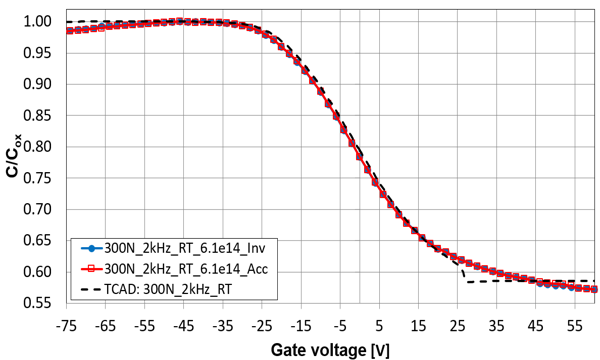
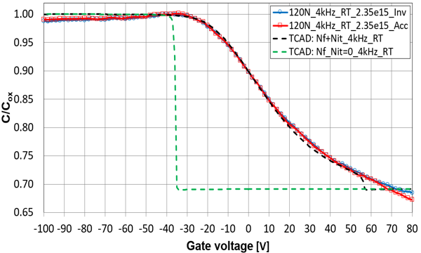
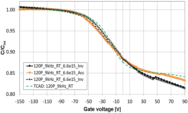
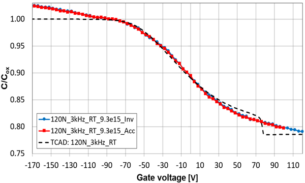
As displayed by the measurements in Figures 3a, 3b, 4a, 5 and 6a, -characteristics of the n/-irradiated MOS-capacitors are distinctly different compared to the results observed before irradiation. The about 1 V-wide depletion regions displayed in Figure 2 have increased to tens of V and has an opposite sign compared to , while hysteresis between -sweeps starting either from accumulation or inversion regions is absent. Additionally, the inversion region has a non-zero slope that is independent of measurement and delay times, and of -sweep direction, while the accumulation region in the initally -bulk MOSs has been reversed to opposite sign gate-voltages () from Figure 2, indicating neutron-irradiation-induced space charge sign inversion (SCSI), where -type Si-bulk is turned effectively to -type by the introduction of acceptor-type bulk defects, switching the majority carriers from electrons to holes. Further signs of the neutron-irradiation-induced displacement damage in the Si-substrate is displayed by the significant increase in the ratio [27, 28] (from 0.3 before irradiation to 0.83 after irradiation, increasing with fluence). The accumulation of displacement damage with neutron irradiation in the Si-bulk of the samples is considered only qualitatively in the scope of this study, while more detailed investigation is presented in [1]. Finally, to produce stable -curves from the n/-irradiated MOSs, careful tuning of the measurement frequency was required, resulting in specific (1–9 kHz) for each of the five investigated fluences. The three -irradiated MOS-capacitors in the study were exposed to doses within uncertainty to the corresponding TID-values of the three neutron irradiated MOSs in Table 4, and were measured at identical frequencies to the n/-irradiated MOSs to enable meaningful comparison.
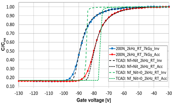
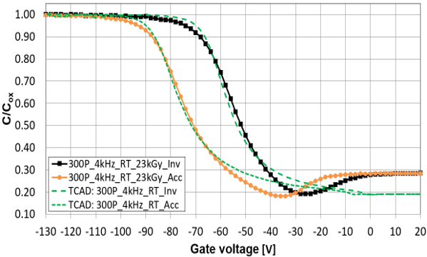
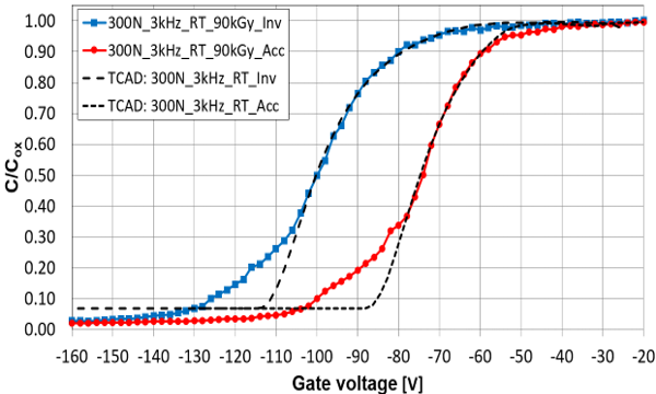
Although the threshold energy for X-rays or gammas to induce bulk damage has been reported to be about 300 keV [6] ( MeV), none of the aforementioned bulk damage effects are visible on the -characteristics of the MOS-capacitors irradiated solely by gammas in Figures 3c, 4b and 6b. The depletion region has again expanded to tens of V, as for n/-irradiated MOSs, but and are now of the same sign, while the -curves starting from the accumulation or inversion regions display significant hysteresis (10 V) that increases with dose. In Figures 3c, 4b and 6b higher absolute value of (= higher positive ) is always seen when -sweep starts from negative . This rules out the influence of , that at negative would always reduce the net value of positive , regardless of the charge sign of .
The comparison between the -irradiated MOS-capacitors with doses within uncertainty to the corresponding MCNP-simulated/interpolated TID-values of the three n/-irradiated MOSs in Table 4 shows systematically lower and -values for the n/-irradiated MOSs, suggesting that the simulated TID-levels at MNRC reactor were overestimated.
To investigate and reproduce the -characteristics of the irradiated MOS-capacitors in Figures 3–6 by TCAD simulation, MOS-structures with input parameters described in Section 3 were applied. For the n/-irradiated MOSs, the occurance of SCSI in -type bulk and the accumulation of the effective bulk doping with neutron fluence were approximated by using -type bulk and tuning to reach similar /-ratios with the measurements, while for -irradiated MOSs, in the absence of displacement damage in the bulk, both - and -bulks were utilized. Simulations were carried out at matching temperature and frequencies to the measurements.
As shown in Figures 3c and 4a, including only (within uncertainty to the measured in Table 5) at the Si/SiO2-interface results in an abrupt depletion region that does not reproduce the characteristics of the measured -curves of either n/- or -irradiated MOS-capacitors. Hence, close agreement between measured and simulated -characteristics was found to require the introduction of both donor- and acceptor-type ( and , respectively) at the interface. Data from previous studies on X-ray irradiated MOS-capacitors and strip sensors [6, 8, 24, 25, 29, 30, 31] was used as a starting point for setting the parameter values of in Table 6, and for further tuning, the surface-state dynamics [2],
| (8) | ||||
where is the interface-trapped charge and is the elementary charge, were considered.
The fully occupied increase the electron density at the Si/SiO2-interface, reducing the net positive oxide charge at the interface, eventually moving from negative to positive with the tuned parameter values presented in Tables 5 and 6. The fully occupied keep the hole density at the interface high enough to widen the depletion region over an extended voltage range with a gradual slope. After the tuning of the parameter values for agreeing -characteristics with the measurements, the densities of both types of in Table 5 remain comparable to the magnitude of , which is in line with previous experimental observations [7, 8, 12]. Additionally, to reproduce the measured -characteristics, it was found to be necessary that both are deep traps, since tuning of one or both with shallow (0.39 eV and 0.48 eV) traps reported in [29] did not produce agreement with the measurements. Also, the of needed to be tuned from the initial eV to eV in Table 6 for a closer match with the experimental results. The trapping cross-section cm2 for deep traps in [29] was not tuned from the initial value for both electrons and holes.
| Sample | -sweep | TCAD | TCAD | TCAD | |
|---|---|---|---|---|---|
| ID | [] | [] | [] | [] | |
| N1(n) | Inv./Acc. | 0.68 | 1.11 | 1.08 | |
| N2(n) | Inv./Acc. | 0.77 | 1.65 | 1.59 | |
| N3(n) | Inv./Acc. | 1.00 | 2.30 | 2.60 | |
| N4(p) | Inv./Acc. | 1.75 | 3.25 | 4.70 | |
| N5(n) | Inv./Acc. | 2.20 | 4.15 | 4.35 | |
| G1(n) | Inv. | 0.79 | 1.92 | 1.10 | |
| Acc. | 0.79 | 1.65 | 1.10 | ||
| G2(p) | Inv. | 1.20 | 1.70 | 1.15 | |
| Acc. | 1.20 | 2.11 | 1.00 | ||
| G3(n) | Inv. | 2.20 | 1.05 | 1.50 | |
| Acc. | 2.00 | 0.50 | 1.00 |
| type | [eV] | [cm2] | Density [cm-2] |
|---|---|---|---|
| Deep donor () | see column 5 in Table 5 | ||
| Deep acceptor () | see column 6 in Table 5 |
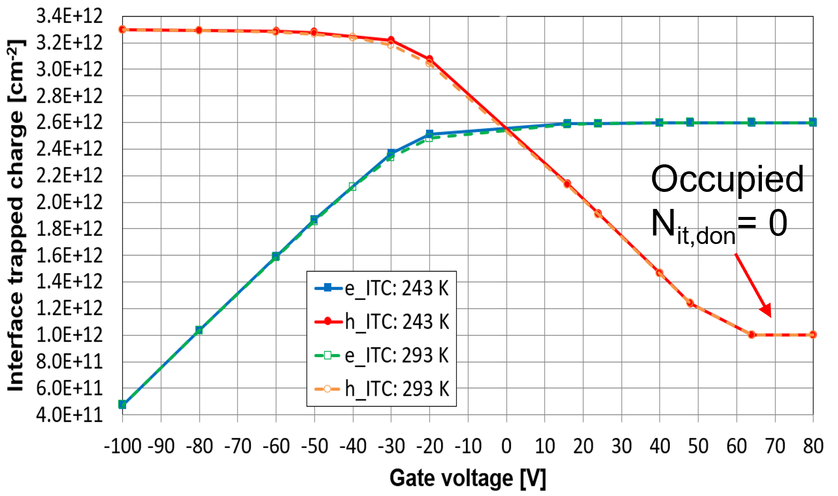
For n/-irradiated MOS-capacitors, the accuracy of the simulation degrades at the highest positive -values in Figures 3a, 3b, 4a and 6a, where an increasing number of minority carriers are pulled to the Si/SiO2-interface. Above , the simulated -curve stabilizes to a constant value in the inversion region, which is not seen in the measurement. This is due to all becoming unoccupied, resulting in the net positive interface charge being composed solely of ( cm-2 in row three of Table 5), as shown in Figure 7a where simulated interface-trapped charge density is displayed as a function of . Thus, in the absence of , the net oxide charge density can be described as
| (9) |
where and are the fractions of fully occupied and , respectively. In Figure 7a, the values of and at -100 V are 1.00 and 0.18, respectively, while at +80 V the corresponding values are 0.0 and 1.0, respectively. This effectively makes in Eq. 9 a dynamic characteristic that experiences polarity change with .
For -irradiated MOS in Figure 4b the measured at deep inversion, showing signs of low-frequency measurement behavior where the inversion-layer charge is supplied/removed quickly enough to respond to changes in (reducing depletion layer depth and increasing inversion towards ) [2], which is not reproduced by the otherwise closely agreeing simulation at kHz. The other visible disagreement between measured and simulated -irradiated MOS-capacitors’ -characteristics is seen in Figure 6b, where the abrupt slope change at about 25 V into depletion-region after in measured -curve is not reproduced by the simulation. This could be evidence of an additional level introduced to the Si/SiO2-interface at high doses, and for - and -bulk MOSs, respectively, that becomes fully occupied at given -value and stops contributing dynamically to the shape of the depletion-region -slope.
Using tuned values of , and , it is possible to analytically find estimates for and in Eq. 9 that produce matching with the measured values in Table 5. By plotting the TCAD-simulated evolution of peak-density-normalized fully occupied and , i.e. interface-trapped charge densities, with in Figure 7b, it is possible to directly extract and at the point of . For -bulk MOS G1(n) in Figure 7b and , resulting in cm-2 (with , and values for -sweep starting from accumulation in Table 5) that is within uncertainty of the measured . Corresponding values of and for MOS N2(n) in the same figure are 0.92 for both, resulting in cm-2, which again is within uncertainty of the measured value. Thus, TCAD simulation and Eq. 9 provide a prediction of the fraction of fully occupied and at , where is extracted.
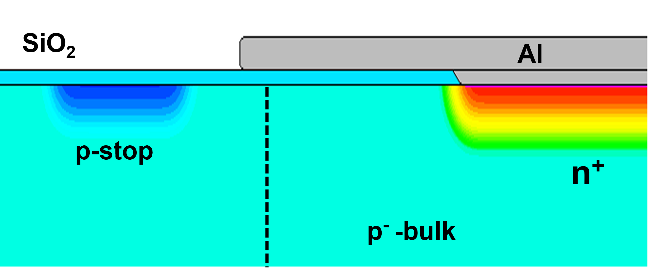
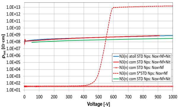
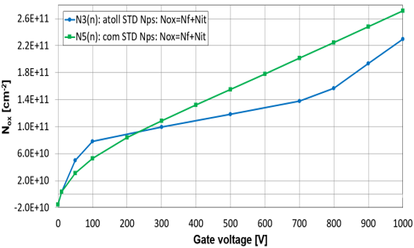
The -dependent dynamic properties of in Eq. 9 can potentially lead to improved isolation of segmented electrodes (e.g. pads, strips, pixels) in irradiated -on- devices, that are in danger of getting shorted at high levels of positive polarity . This was investigated in Figure 8 by using , and in Table 5, tuned to the measured -characteristics of the MOS-capacitors N3(n) (with ) and N5(n) (with ) as an input at the Si/SiO2-interface for an inter-strip resistance ()-simulation of a -on- sensor structure in Figure 8a. Displayed in Figure 8b, high levels of () are maintained throughout the investigated reverse bias -range ( kV), for the ‘standard’ value of -stop peak doping (STD ) and regardless of the -stop configuration. Both the voltage dependence and absolute values of are in close agreement with previously reported experimental results of X-ray [15] and reactor [32, 33] irradiated strip-sensors, while the gradual decay of measured with fluence is also reproduced. By excluding and from the simulation, the strips become either shorted (STD , in Figure 8b) for all voltages or reach isolation only above 500 V of for an extreme value of -stop peak doping ( , ).
Figure 8c shows the effect of fully occupied on in the inter-strip region with the evolution of the positive potential at the strip electrode. For the MOS-capacitor N3(n), after polarity change from negative to positive between 0–10 V the values of at the Si/SiO2-interface only increase beyond pre-irradiated levels in Table 3 above 700 V, resulting in high throughout the -range. Even though keeps increasing above (for N3(n) between 0–1 kV and in Eq. 9 change from 0.679 and 0.991 to 0.782 and 0.988, respectively), the corresponding in Figure 8b keeps growing, since electrons are getting increasingly swiped from the inter-strip region to the strip-electrodes at extreme voltages. The decay of for the higher fluence N5(n) from the levels observed for N3(n) in Figure 8b, is reflected by the higher values of at V. Hence, the experimentally observed high -values in irradiated -on- strip-sensors can be explained by the beneficial effect to from the radiation-induced accumulation of . Similar observations have been reported in previous simulation studies [15, 34] with varied approaches in the application of .
5 Discussion
The -dependence of the irradiated MOS-capacitor -characteristics is introduced by the capture and emission rates of [2], which is opposite for and . Thus, at increased a larger fraction of and are fully occupied and unoccupied, respectively, leading to higher positive net oxide charge at Si/SiO2-interface, while at decreased the trap occupation is reversed, resulting in lower positive and therefore lower negative gate voltage produces the flat-band condition in both - and -bulk devices. Additionally, the Boltzmann statistics of deep-trap-level introduces significant temperature dependence (, where is the activation energy of the trap) [2], when the capture and emission rates slow down with lower and measurements with constant result in substantially different and -characteristics already within C. These compromise the assessment of any fluence or dose-dependence of the Si/SiO2-interface properties from MOS -characteristics, since the results are only valid for the given measurement and . Frequency dependence changes also with the densities of , thus no conclusions on the evolution of the oxide-interface properties between n/- and -irradiated MOS-capacitors or between different fluences and doses are included in this study.
6 Summary and conclusions
Combined experimental and simulation -characterization study of MOS-capacitor samples diced from 6-inch wafers –with about 700-nm-thick gate oxides– suggests that at the Si/SiO2-interface changes from being dominated by before irradiation to include both deep donor- ( eV) and deep acceptor-type ( eV) , with comparable densities to , after being exposed to either a -source or to a reactor radiation environment. This was found by the process of reproducing the measured -characteristics of five n/-irradiated and three -irradiated MOS-capacitors by a TCAD-simulation, where close agreement between measurement and simulation were only reached when in addition to , both and were included in the tuning.
Due to the -dependence of the fraction of the fully occupied and , the dynamic nature of can explain the experimentally observed high levels of inter-electrode resistance in irradiated -on- devices, like strip-sensors. An -simulation of a -on- strip-sensor structure using , and (tuned to reproduce the -characteristics of an irradiated MOS-capacitor) as an input, showed close agreement for both the voltage dependence and absolute values of with previously reported experimental results of X-ray and reactor irradiated strip-sensors. High values of simulated were due to the low levels of in the inter-strip region between the strip-anodes.
Thus, the simulation study provides two separate observations of the macroscopic effects of the radiation-induced accumulation of at the Si/SiO2-interface that can explain the experimental results. The -accumulation-generated beneficial impact on inter-electrode isolation in irradiated -on- sensors suggests that very high levels of -stop peak doping () could be avoided, mitigating the probability of discharges or avalanche effects due to excessive electric fields at the -stops in the extreme radiation environment of the foreseen high-luminosity LHC.
Acknowledgements
This work has been supported by the US Department of Energy, Office of Science (DE-SC0015592). We thank the HGCAL and CMS Tracker collaborations of the CMS Experiment for providing the samples investigated in this study. We thank K. Zinsmeyer, C. Perez, and posthumously P. Cruzan of TTU for their expert technical support.
References
- [1] T. Peltola, et al., Charge Collection and Electrical Characterization of Neutron Irradiated Silicon Pad Detectors for the CMS High Granularity Calorimeter, JINST 15 (2020) P09031. doi:10.1088/1748-0221/15/09/P09031.
- [2] E. H. Nicollian, J. R. Brews, MOS (Metal Oxide Semiconductor) Physics and Technology, John Wiley & Sons, New York NY U.S.A., 1982.
- [3] T. P. Ma, P. V. Dressendorfer, Ionizing Radiation Effects in MOS Devices and Circuits, John Wiley & Sons, New York NY U.S.A., 1989.
- [4] T. R. Oldham, Ionizing Radiation Effects in MOS Oxides, World Scientific Publishing, Singapore, 1999.
- [5] J. R. Schwank, et al., Radiation Effects in MOS Oxides, IEEE Trans. Nucl. Sci. 55 (4) (2008) 1833–1853. doi:10.1109/TNS.2008.2001040.
- [6] J. Zhang, et al., Investigation of X-ray induced radiation damage at the Si-SiO2 interface of silicon sensors for the European XFEL, JINST 7 (2012) C12012. doi:10.1088/1748-0221/7/12/C12012.
- [7] S. Kim, et al., The effects of X-ray irradiation-induced damage on reliability in MOS structures, Solid-State Electronics 38 (1995) 95–99. doi:10.1016/0038-1101(94)E0054-I.
-
[8]
J. Zhang,
X-ray
Radiation Damage Studies and Design of a Silicon Pixel Sensor for Science at
the XFEL, Ph.D. thesis, University of Hamburg (2013).
URL https://bib-pubdb1.desy.de/record/152137/files/DESY-2013-00115.pdf - [9] G. Verzellesi, G.-F. D. Betta, G. Pignatel, Compact modeling of n-side interstrip resistance in p-stop and p-spray isolated double-sided silicon microstrip detectors, in: 2000 IEEE Nuclear Science Symposium, IEEE, Lyon, France, 2000, pp. 25–27. doi:10.1109/NSSMIC.2000.949004.
- [10] C. Piemonte, Device simulations of isolation techniques for silicon microstrip detectors made on p-type substrates, IEEE Trans. Nucl. Sci NS-53 (2006) 1694–1705. doi:10.1109/TNS.2006.872500.
- [11] Y. Unno, et al., Optimization of surface structures in n-in-p silicon sensors using TCAD simulation, Nucl. Instr. Meth. A 636 (2011) 118–124. doi:10.1016/j.nima.2010.04.095.
- [12] R. Dalal, et al., Simulation of irradiated Si detectors, PoS 030 (2014) (VERTEX2014). doi:10.22323/1.227.0030.
- [13] A. Morozzi, F. Moscatelli, D. Passeri, G. M. Bilei, TCAD advanced radiation damage modeling in silicon detectors, PoS 050 (2020) (VERTEX2019). doi:10.22323/1.373.0050.
- [14] A. Morozzi, F. Moscatelli, T. Croci, D. Passeri, TCAD Modeling of Surface Radiation Damage Effects: A State-Of-The-Art Review, Front. in Phys. 9 (2021) 617322. doi:10.3389/fphy.2021.617322.
- [15] F. Moscatelli, D. Passeri, A. Morozzi, S. Mattiazzo, G. F. Dalla Betta, M. Dragicevic, G. M. Bilei, Effects of Interface Donor Trap States on Isolation Properties of Detectors Operating at High-Luminosity LHC, IEEE Trans. Nucl. Sci. 64 (8) (2017) 2259–2267. doi:10.1109/TNS.2017.2709815.
-
[16]
R. Eber,
Investigations
of new sensor designs and development of an effective radiation damage model
for the simulation of highly irradiated silicon particle detectors, Ph.D.
thesis, Karlsruhe Institute of Technology (2013).
URL http://digbib.ubka.uni-karlsruhe.de/volltexte/1000038403 - [17] T. Peltola, et al., A method to simulate the observed surface properties of proton irradiated silicon strip sensors, JINST 10 (2015) C04025. doi:10.1088/1748-0221/10/04/C04025.
-
[18]
T. Peltola,
Numerical
simulations of semiconductor radiation detectors for high-energy physics and
spectroscopy applications, Ph.D. thesis, University of Helsinki (2016).
URL https://helda.helsinki.fi/bitstream/handle/10138/159441/numerica.pdf?sequence=1 - [19] S. M. Sze, Physics of Semiconductor Devices, 2nd Edition, John Wiley & Sons, Hoboken New Jersey U.S.A., 1981.
- [20] G. Greeuw, J. F. Verwey, The mobility of Na+, Li+, and K+ ions in thermally grown SiO2 films, J. Appl. Phys. 56 (8) (1984) 2218–2224. doi:10.1063/1.334256.
- [21] A. J. Suria, H. C. Chiamori, A. Shankar, D. G. Senesky, Capacitance-voltage characteristics of gamma irradiated Al2O3, HfO2, and SiO2 thin films grown by plasma-enhanced atomic layer deposition, in: Sensors for Extreme Harsh Environments II, Vol. 9491, SPIE, 2015, pp. 6 – 13. doi:10.1117/12.2179129.
- [22] P. O. Oviroh, et al., New development of atomic layer deposition: processes, methods and applications, Sci. Technol. Adv. Mater. 20 (1) (2019) 465 – 496. doi:10.1080/14686996.2019.1599694.
- [23] R. C. Jaeger, Introduction to Microelectronic Fabrication, Vol. 5, in The Modular Series on Solid State Devices, 2nd Edition, Addison-Wesley, 2002.
- [24] T. Poehlsen, et al., Charge losses in segmented silicon sensors at the Si-SiO2 interface, Nucl. Instr. Meth. A 700 (2013) 22–39. doi:10.1016/j.nima.2012.10.063.
- [25] J. Zhang, et al., X-ray induced radiation damage in segmented p+n silicon sensors, PoS 019 (2012) (VERTEX2012). doi:10.22323/1.167.0019.
- [26] T. Peltola, Simulation of radiation-induced defects, PoS 031 (2015) (VERTEX2015). doi:10.22323/1.254.0031.
- [27] P. Fernández-Martínez, et al., Analysis of displacement damage effects on MOS capacitors, Nucl. Instr. Meth. A 730 (2013) 91–94. doi:10.1016/j.nima.2013.05.108.
-
[28]
J. A. Luna-López, M. Aceves-Mijares, O. Malik, R. Glaenzer,
Modelling the C-V
characteristics of MOS capacitor on high resistivity silicon substrate for
PIN photodetector applications, Revista Mexicana de Fisica 52 (2) (2006)
45–47.
URL https://www.researchgate.net/publication/242092497 - [29] J. Zhang, et al., Study of radiation damage induced by 12 keV X-rays in MOS structures built on high-resistivity -type silicon, J. Synchrotron Rad. 19 (2012) 340–346. doi:10.1107/S0909049512002348.
- [30] T. Poehlsen, et al., Study of the accumulation layer and charge losses at the Si-SiO2 interface in p+n-silicon strip sensors, Nucl. Instr. Meth. A 721 (2013) 26–34. doi:10.1016/j.nima.2013.04.026.
-
[31]
T. Pöhlsen, Charge Losses in
Silicon Sensors and Electric-Field Studies at the Si-SiO2 Interface,
Ph.D. thesis, University of Hamburg (2013).
URL https://cds.cern.ch/record/1604839 - [32] The Tracker Group of the CMS Collaboration, P-Type Silicon Strip Sensors for the new CMS Tracker at HL-LHC, JINST 12 (2017) P06018. doi:10.1088/1748-0221/12/06/P06018.
- [33] The Tracker Group of the CMS Collaboration, Experimental study of different silicon sensor options for the upgrade of the CMS Outer Tracker, JINST 15 (2020) P04017. doi:10.1088/1748-0221/15/04/P04017.
-
[34]
J.-O. Müller-Gosewisch,
Investigation of Radiation
Damage in Silicon Sensors for the Phase-2 Upgrade of the CMS Outer Tracker,
Ph.D. thesis, KIT, Karlsruhe, ETP (2021).
URL https://publish.etp.kit.edu/record/22097