Self-probed ptychography from semiconductor high-harmonic generation
Abstract
We demonstrate a method to image an object using a self-probing approach based on semiconductor high-harmonic generation. On one hand, ptychography enables high-resolution imaging from the coherent light diffracted by an object. On the other hand, high-harmonic generation from crystals is emerging as a new source of extreme-ultraviolet ultrafast coherent light. We combine these two techniques by performing ptychography measurements with nano-patterned crystals serving as the object as well as the generation medium of the harmonics. We demonstrate that this strong field in situ approach can provide structural information about the object. With the future developments of crystal high harmonics as a compact short-wavelength light source, our demonstration can be an innovative approach for nanoscale imaging of photonic and electronic devices in research and industry.
Imagine Optic, 18, rue Charles de Gaulle, 91400 ORSAY, France \alsoaffiliationGoLP, Instituto de Plasmas e Fusão Nuclear, Instituto Superior Técnico, Universidade de Lisboa, 1049-001 Lisboa, Portugal \alsoaffiliationUniversité de Limoges, CNRS, XLIM, UMR 7252, 87000 Limoges, France \alsoaffiliationLOA, ENSTA ParisTech, CNRS, Ecole Polytechnique, UMR 7639, 828 Boulevard des Maréchaux, 91120 Palaiseau, France
KEYWORDS: diffractive imaging, high-harmonic generation, nanostructured semiconductors, nano-optics, ultrafast photonics
1 Introduction
Since its first observation 1 high-harmonic generation (HHG) from band gap solids has been an intensively studied topic that opens up to a wide range of applications. The all-solid-state nature of the generating medium enables more compact UV to extreme-ultraviolet (XUV) HHG sources. Additionally, the harmonics generated from the strong field interaction with the solid are highly sensitive to its electronic band structure, making them an excellent observable for structural properties of the material 2. Furthermore, the visualization of the electron currents associated to the fundamental mechanisms of the strong field process can pave the way for applications in future petahertz optoelectronics 3, 4, 5 or light induced topology 6, 7. Over the past years high harmonics have been observed in a multitude of materials ranging from 3D bulk 1, 8, 9, 10 to 2D crystals 11, 12, 13. Out of the many possibilities, nanostructuring of the material is especially interesting as it allows to increase the generated harmonic yield and directly control the spatial structure of the generated harmonics 14, 15, 6, 16. The sub-wavelength sensitivity of the generating beam to those nanostructures can be further exploited to monitor nanoscale spatial amplitude and phase modulations of the crystal itself.
Coherent diffractive imaging (CDI) is a powerful technique that has been widely used for nanoscale imaging since its first experimental demonstration 17. By solving the so-called phase problem, using a phase retrieval algorithm, this lensless technique can reach a spatial resolution limited only by the wavelength. Ptychography was developed to generalize CDI to extended objects 18. It uses multiple coherent diffraction patterns originating from overlapping light probes on the structure. The image reconstruction of the whole structure is performed using the redundant information provided by these multiple diffraction patterns using an iterative algorithm 19, 20. Stunning demonstrations have been performed using synchrotron radiation or HHG-gas sources in biology and solids state physics 18, 21, 22, 23, 24, 25.
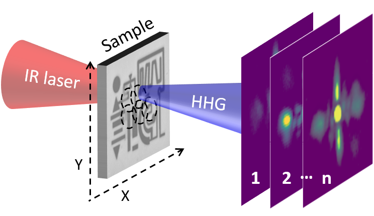
In this work we demonstrate the use of HHG from solids as an integrated source of light to image a sample using ptychography. The key here is to combine in a 2-in-1 configuration the generation medium and the object, as illustraded in Figure 1. In this configuration, the ptychographic HHG probe is intricated with the object. Indeed HHG from solids is a spatially coherent light source that qualifies also well for coherent diffractive imaging as was demonstrated recently 15. The conservation of the coherence properties during the generation process makes the harmonics a suitable intrinsic self-probe for ptychography. Compared to a previous work that uses the perturbative second harmonic generation 26, the non-perturbative high-harmonic generation allows to image the object with significant structural information thanks to the sensitivity of the strong field emission process to the material properties. Finally, another interest of the ptychographic approach is the compatibility with tight focusing. This enables low average power femtosecond fiber lasers to reach sufficient intensities for HHG in solids and opens up possibilities for extremely compact and affordable arrangements.
2 Methods
In our experiments we use a commercial all-fiber laser delivering 90 fs pulses with 10 nJ at a central wavelength of 2100 nm and 18.66 MHz repetition rate, having linearly polarized purely single mode output beam 27. The laser beam is focused at the rear side of the sample by an aspheric lens with 3 cm focal length, reaching a focal spot size of 6.5 µm (FWHM), with intensities of about 0.2 TW/cm2. Self-focusing during the propagation of the beam in the sample can additionally decrease the laser focus and furhter increase the peak intensity. The fifth harmonic order at a wavelength of 420 nm is selected using a bandpass filter set just before the CCD camera. Because of mechanical limitations and of the limited chip size of the CCD, a microscope objective (numerical aperture (NA) of 0.75) is set after the sample collecting the wide angle diffraction patterns on the detector. It images the far field diffraction pattern from a virtual plane located about 200 µm after the sample.

The raw ptychographic data are pre-processed before the reconstruction, this includes: i) binning and cropping of the diffraction pattern, ii) subtraction of background noise and iii) correction for the projection of the Ewald sphere onto the flat detector. As a consequence of this pre-processings, the effective NA of the diffraction data set is limited to 0.5. The calibration of the microscope objective magnification (of about 20) is performed by comparing the experimental data to numerical simulations. The ptychographic data were then used to perform the amplitude and phase image reconstruction of the nano-patterned samples using the PyNX library 28.
3 Results and discussion
3.1 Nanopatterned silicon sample
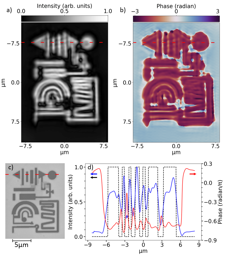
The first structure is patterned onto a 300 µm (100)-cut silicon sample using a Focused Ion Beam (FIB). The test geometry is a custom mix of features commonly used in scientific and industrial applications (see Figure 2 (c)). Its overall size is 18x12 µm2. The depth is chosen to be about 50 nm to achieve a well contrasted phase object. The structure is probed in a spiral scanning pattern using 2000 points with an average step size of 500 nm and with 3 seconds of integration time each. The polarization of the laser is aligned along the short axis of the structure that matches the [110]-axis (K) of the silicon sample. The reconstruction uses 40 iterations of the alternating projections algorithm followed by 40 iterations of maximum likelihood algorithm retrieving the probe simultaneously with the image of the object. The reconstructions are performed on a GPU using PyNX CUDA supported modules. To avoid artifacts of the reconstruction process, 10 independent reconstructions are averaged. The retrieved probe, that reconstructs the harmonic source, has a size of 2.5 µm (FWHM). The size reduction in respect to the laser focus results from the self-focusing effect and from the harmonic nonlinear conversion.

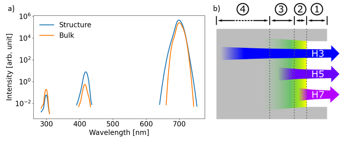
An example of a reconstruction in amplitude and phase of the sample is shown in Figure 2. It retrieves all the features of the sample. A resolution of 800 nm is estimated using a 10%-90% edge criterion on the rightmost edge of the amplitude in Figure 2 (d), which is less than twice the theoretical resolution limit for this setup (). The comparison of the cut through the reconstructed structure with a cut through the original pattern shows a good overlap. We note the presence of unexpected amplitude modulations in the reconstruction. This effect takes its origin in the propagation of H5 in the structure 29 and is qualitatively confirmed by finite difference time domain (FDTD) simulations. Moreover, the simulation of the propagation of the fundamental laser confirms no significant confinement in the 50 nm depth nanostructures. The overall phase profile shows a contrast of 0.95, close to the designed phase difference of . However, The amplitude reveals an increase of the coherent signal from the patterned area compared to the unpatterned parts of the sample by tenfold that does not match the expected design of a phase object. Comparative spectroscopic measurements of the HHG emission between the structured sample and the bulk material have been conducted and have confirmed this increase of the harmonic 5 signal from the patterned sample (Figure 3 (a)). This behaviour is also visible for H3, which is slightly increased. In contrast H7, the first above band gap harmonic, is decreased significantly.

This increase of below band gap harmonics was observed by Sivis et al 14 for FIB induced Ga+ ion implantation as well. However the ion dose (at 30 keV) used to etch the structures in our work is larger, leading to a higher relative fraction of Ga ions of up to 0.1 30. The process also generates secondary effects like the amorphization of the crystal structure close to the surface 30, 31, 32. This effect can create tails of localized states into the bands 33, while the doping, as well as the crystal defects (e.g. vacancies) occurring alongside, add defect bands in the band gap or can even modify the band gap itself. The increase in signal for the below band gap harmonics (H3 and H5) could result from an increased probability of interband transitions (photon emission from the electron-hole recombination) from those additional states present in the band gap of the pristine silicon. This is particularly true for H5 whose energy is close to the band gap energy. Theoretical studies have reported such enhancement for below band gap harmonics, in the case of pure doping and vacancies 34, 35. However, crystal amorphization has been studied theoretically and experimentally and have been found to significantly lower the HHG yield 36, 37. Thus, the enhancement of below band gap harmonics is counter-acted by the overall HHG signal reduction due to the amorphization. Additionally, each harmonic experiences a different absorption by the material. This absorption also depends on the changes induced by the FIB and consequently changes with depth. All together, the measured part for each harmonic is generated up to a different depth and experiences a different sensitivity to the material changes as sketched Figure 3 (b). For our case H3 is generated at a large depth and is therefore less affected than H5 and H7 that are generated closer to the surface.
3.2 Spiral zone plate patterned on ZnO

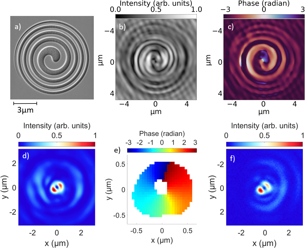
As a second test of the capabilities of ptychography with HHG from solids, we studied a 10x10 µm2 spiral zone plate (SZP) patterned on a 500 µm thick zinc oxide (ZnO) crystal. The structure is designed to generate a Laguerre-Gaussian beam carrying an orbital angular momentum (OAM) without the need to pre-shape the driving IR field 6. An example of an SZP is shown in Figure 4 (a). It is designed to be a pure phase object combining the phase profiles of helical and spherical waves to induce the OAM and focus the beam 6 µm after the structure. The harmonic used for the measurements is again H5 which lies below the band gap energy of ZnO (3.3 eV) and is hence generated in the bulk before being diffracted by the SZP. The etching depth is chosen to be 210 nm resulting in a phase step of . Measurements are performed under similar conditions as for the silicon sample, but scanning the sample in a grid pattern with an average step size of 400 nm. We attempt to retrieve the induced OAM from the patterned structure based on the ptychography measurements similar to the approach presented by Vila Comamala et al 38. The data were reconstructed using a combination of algorithms with a total of 210 iterations of alternating projections and 10 iterations of difference map, performed using the CPU supported module of PyNX.
The results of the complex field at the exit of the SZP in amplitude and phase are shown in Figure 4 (b) and (c). The expected well contrasted binary phase profile is retrieved within the boundaries of the scanned area. This object behaves closely as a pure phase object with a low amplitude contrast between the patterned and non-patterned areas, a behaviour that can be explained by the higher resistance of ZnO to material alterations in the FIB process 39. Amplitude vs. phase contrast are clearly target dependant, emphasising the potential of this technique for elemental mapping. However, as the ZnO sample features a much deeper structure than the silicon, the amplitude picture shows a double spiral as a results of the strong propagation effects expected for both the fundamental and H5, which is in qualitative agreement with FDTD simulations. The stronger confinement effect in the structure from the vertical polarization is particularly visible. The numerical propagation of the reconstructed complex field to the focal plane of the SZP is shown in Figure 4 (d) and (e). It matches the result from our previous experiments in [6] (reproduced in Figure 4 (f)). We retrieve the same aberration due to the limited number of illuminated diffracting zones from the structure. In addition, we access the phase profile that confirms the OAM carried by the focused beam.
4 Conclusion
In conclusion, we demonstrated that self-probed ptychography allows for robust reconstruction of various structures and can be a valuable asset for the characterization of nanostructures or meta-optics in the context of HHG from solids. This approach can be scaled towards the cutoff of HHG from solids, reaching currently 50 nm 8, which translates directly into a gain of resolution. Additionally, the sensitivity of the HHG mechanisms based on the non-perturbative nonlinear properties of the material to the driving laser field can give access to valuable spectroscopic information from the reconstructed image. In combination with the recent potential in multi-wavelength imaging 40, self-probed ptychography could allow a full access to the spatio-spectral image of the sample. Finally, high spatial and temporal resolution could be obtained in conjunction with broadband CDI algorithms 41.
5 Funding
We acknowledge the financial support from the PETACom FET Open H2020 grant No. 829153/ OPTOLogic grant No. 899794/ TSAR grant No. 964931 and EIC Open grant No. 101047223-NanoXCAN. We acknowledge the financial support from the French ANR through the grants PACHA (ANR-17-CE30-0008-01), FLEX-UV (ANR-20-CE42-0013-02) and ATTOCOM (ANR-21-CE30-0036-02). We acknowledge the financial support from the French ASTRE program through the “NanoLight” grant. This work was partially supported by the Fundação para a Ciência e Tecnologia (grant No. PD/BD/135224/2017).
6 Acknowledgments
We thank Vincent Favre-Nicolin and Kadda Medjoubi for the valuable advice and discussions regarding the reconstructions and PyNX library. We thank Juliana Tiburcio, Reda Berrada and Vijay Sunuganty for the fruitful discussions. We acknowledge Franck Fortuna and the use of the SEM-FIB facility of the Institut des Sciences Moléculaires d’Orsay, for the sample structurations.
7 Notes
The authors declare no competing financial interest.
8 Data availability
The data are available from the corresponding author upon reasonable request.
References
- Ghimire et al. 2011 Ghimire, S.; DiChiara, A. D.; Sistrunk, E.; Agostini, P.; DiMauro, L. F.; Reis, D. A. Observation of high-order harmonic generation in a bulk crystal. Nature Physics 2011, 7, 138–141
- Vampa et al. 2015 Vampa, G.; Hammond, T.; Thiré, N.; Schmidt, B.; Légaré, F.; McDonald, C.; Brabec, T.; Klug, D.; Corkum, P. All-Optical Reconstruction of Crystal Band Structure. Physical Review Letters 2015, 115, 193603
- Krausz and Stockman 2014 Krausz, F.; Stockman, M. I. Attosecond metrology: from electron capture to future signal processing. Nature Photonics 2014, 8, 205–213
- Schoetz et al. 2019 Schoetz, J.; Wang, Z.; Pisanty, E.; Lewenstein, M.; Kling, M. F.; Ciappina, M. F. Perspective on Petahertz Electronics and Attosecond Nanoscopy. ACS Photonics 2019,
- Sederberg et al. 2020 Sederberg, S.; Zimin, D.; Keiber, S.; Siegrist, F.; Wismer, M. S.; Yakovlev, V. S.; Floss, I.; Lemell, C.; Burgdörfer, J.; Schultze, M.; Krausz, F.; Karpowicz, N. Attosecond optoelectronic field measurement in solids. Nature Communications 2020, 11, 1–8
- Gauthier et al. 2019 Gauthier, D.; Kaassamani, S.; Franz, D.; Nicolas, R.; Gomes, J.-T.; Lavoute, L.; Gaponov, D.; Février, S.; Jargot, G.; Hanna, M.; Boutu, W.; Merdji, H. Orbital angular momentum from semiconductor high-order harmonics. Optics Letters 2019, 44, 546–549
- Silva et al. 2019 Silva, R. E. F.; Jiménez-Galán, A.; Amorim, B.; Smirnova, O.; Ivanov, M. Topological strong-field physics on sub-laser-cycle timescale. Nature Photonics 2019, 13, 849–854
- Luu et al. 2015 Luu, T. T.; Garg, M.; Kruchinin, S. Y.; Moulet, A.; Hassan, M. T.; Goulielmakis, E. Extreme ultraviolet high-harmonic spectroscopy of solids. Nature 2015, 521, 498–502
- Kim et al. 2017 Kim, H.; Han, S.; Kim, Y. W.; Kim, S.; Kim, S.-W. Generation of Coherent Extreme-Ultraviolet Radiation from Bulk Sapphire Crystal. ACS Photonics 2017, 4, 1627–1632
- Nefedova et al. 2021 Nefedova, V. E. et al. Enhanced extreme ultraviolet high-harmonic generation from chromium-doped magnesium oxide. Applied Physics Letters 2021, 118, 201103
- Yoshikawa et al. 2017 Yoshikawa, N.; Tamaya, T.; Tanaka, K. High-harmonic generation in graphene enhanced by elliptically polarized light excitation. Science 2017, 356, 736–738
- Liu et al. 2017 Liu, H.; Li, Y.; You, Y. S.; Ghimire, S.; Heinz, T. F.; Reis, D. A. High-harmonic generation from an atomically thin semiconductor. Nature Physics 2017, 13, 262–265
- Hafez et al. 2018 Hafez, H. A. et al. Extremely efficient terahertz high-harmonic generation in graphene by hot Dirac fermions. Nature 2018, 561, 507–511
- Sivis et al. 2017 Sivis, M.; Taucer, M.; Vampa, G.; Johnston, K.; Staudte, A.; Naumov, A. Y.; Villeneuve, D. M.; Ropers, C.; Corkum, P. B. Tailored semiconductors for high-harmonic optoelectronics. Science 2017, 357, 303–306
- Franz et al. 2019 Franz, D. et al. All semiconductor enhanced high-harmonic generation from a single nanostructured cone. Scientific Reports 2019, 9, 5663
- Liu et al. 2020 Liu, H.; Vampa, G.; Zhang, J. L.; Shi, Y.; Buddhiraju, S.; Fan, S.; Vuckovic, J.; Bucksbaum, P. H.; Reis, D. A. Beating absorption in solid-state high harmonics. Communications Physics 2020, 3, 1–6
- Miao et al. 1999 Miao, J.; Charalambous, P.; Kirz, J.; Sayre, D. Extending the methodology of X-ray crystallography to allow imaging of micrometre-sized non-crystalline specimens. Nature 1999, 400, 342–344
- Pfeiffer 2018 Pfeiffer, F. X-ray ptychography. Nature Photonics 2018, 12, 9–17
- Rodenburg and Faulkner 2004 Rodenburg, J. M.; Faulkner, H. M. L. A phase retrieval algorithm for shifting illumination. Applied Physics Letters 2004, 85, 4795–4797
- Thibault et al. 2008 Thibault, P.; Dierolf, M.; Menzel, A.; Bunk, O.; David, C.; Pfeiffer, F. High-resolution scanning x-ray diffraction microscopy. Science (New York, N.Y.) 2008, 321, 379–382
- Holler et al. 2017 Holler, M.; Guizar-Sicairos, M.; Tsai, E. H. R.; Dinapoli, R.; Müller, E.; Bunk, O.; Raabe, J.; Aeppli, G. High-resolution non-destructive three-dimensional imaging of integrated circuits. Nature 2017, 543, 402–406
- Giewekemeyer et al. 2010 Giewekemeyer, K.; Thibault, P.; Kalbfleisch, S.; Beerlink, A.; Kewish, C. M.; Dierolf, M.; Pfeiffer, F.; Salditt, T. Quantitative biological imaging by ptychographic x-ray diffraction microscopy. Proceedings of the National Academy of Sciences 2010, 107, 529–534
- Shi et al. 2016 Shi, X.; Fischer, P.; Neu, V.; Elefant, D.; Lee, J. C. T.; Shapiro, D. A.; Farmand, M.; Tyliszczak, T.; Shiu, H.-W.; Marchesini, S.; Roy, S.; Kevan, S. D. Soft x-ray ptychography studies of nanoscale magnetic and structural correlations in thin SmCo5 films. Applied Physics Letters 2016, 108, 094103
- Baksh et al. 2016 Baksh, P. D.; Odstrčil, M.; Kim, H.-S.; Boden, S. A.; Frey, J. G.; Brocklesby, W. S. Wide-field broadband extreme ultraviolet transmission ptychography using a high-harmonic source. Optics Letters 2016, 41, 1317–1320
- Loetgering et al. 2021 Loetgering, L.; Loetgering, L.; Loetgering, L.; Liu, X.; Liu, X.; Beurs, A. C. C. D.; Beurs, A. C. C. D.; Du, M.; Du, M.; Kuijper, G.; Eikema, K. S. E.; Eikema, K. S. E.; Witte, S.; Witte, S. Tailoring spatial entropy in extreme ultraviolet focused beams for multispectral ptychography. Optica 2021, 8, 130–138
- Odstrcil et al. 2016 Odstrcil, M.; Baksh, P.; Gawith, C.; Vrcelj, R.; Frey, J. G.; Brocklesby, W. S. Nonlinear ptychographic coherent diffractive imaging. Opt. Express 2016, 24, 20245–20252
- 27 NOVAE Brevity. \urlhttps://www.novae-laser.com/brevity/
- Favre-Nicolin et al. 2020 Favre-Nicolin, V.; Girard, G.; Leake, S.; Carnis, J.; Chushkin, Y.; Kieffer, J.; Paleo, P.; Richard, M.-I. PyNX: high-performance computing toolkit for coherent X-ray imaging based on operators. Journal of Applied Crystallography 2020, 53, 1404–1413
- Zayko et al. 2015 Zayko, S.; Mönnich, E.; Sivis, M.; Mai, D.-D.; Salditt, T.; Schäfer, S.; Ropers, C. Coherent diffractive imaging beyond the projection approximation: waveguiding at extreme ultraviolet wavelengths. Optics Express 2015, 23, 19911–19921
- Gnaser et al. 2008 Gnaser, H.; Brodyanski, A.; Reuscher, B. Focused ion beam implantation of Ga in Si and Ge: fluence-dependent retention and surface morphology. Surface and Interface Analysis 2008, 40, 1415–1422
- Lehrer et al. 2001 Lehrer, C.; Frey, L.; Petersen, S.; Ryssel, H. Limitations of focused ion beam nanomachining. Journal of Vacuum Science & Technology B: Microelectronics and Nanometer Structures Processing, Measurement, and Phenomena 2001, 19, 2533–2538
- Schrauwen et al. 2007 Schrauwen, J.; Van Thourhout, D.; Baets, R. Iodine enhanced focused-ion-beam etching of silicon for photonic applications. Journal of Applied Physics 2007, 102, 103104
- Horowitz 2015 Horowitz, G. Validity of the concept of band edge in organic semiconductors. Journal of Applied Physics 2015, 118, 115502
- Pattanayak et al. 2020 Pattanayak, A.; Mrudul, M. S.; Dixit, G. Influence of vacancy defects in solid high-order harmonic generation. Physical Review A 2020, 101, 013404
- Mrudul et al. 2020 Mrudul, M. S.; Tancogne-Dejean, N.; Rubio, A.; Dixit, G. High-harmonic generation from spin-polarised defects in solids. npj Computational Materials 2020, 6, 1–9
- Orlando et al. 2018 Orlando, G.; Wang, C.-M.; Ho, T.-S.; Chu, S.-I. High-order harmonic generation in disordered semiconductors. JOSA B 2018, 35, 680–688
- You et al. 2017 You, Y. S.; Yin, Y.; Wu, Y.; Chew, A.; Ren, X.; Zhuang, F.; Gholam-Mirzaei, S.; Chini, M.; Chang, Z.; Ghimire, S. High-harmonic generation in amorphous solids. Nature Communications 2017, 8, 724
- Vila-Comamala et al. 2014 Vila-Comamala, J.; Sakdinawat, A.; Guizar-Sicairos, M. Characterization of x-ray phase vortices by ptychographic coherent diffractive imaging. Opt. Lett. 2014, 39, 5281–5284
- Kucheyev et al. 2003 Kucheyev, S. O.; Williams, J. S.; Jagadish, C.; Zou, J.; Evans, C.; Nelson, A. J.; Hamza, A. V. Ion-beam-produced structural defects in ZnO. Physical Review B 2003, 67, 094115
- Rana et al. 2020 Rana, A.; Zhang, J.; Pham, M.; Yuan, A.; Lo, Y. H.; Jiang, H.; Osher, S. J.; Miao, J. Potential of Attosecond Coherent Diffractive Imaging. Phys. Rev. Lett. 2020, 125, 086101
- Huijts et al. 2020 Huijts, J.; Fernandez, S.; Gauthier, D.; Kholodtsova, M.; Maghraoui, A.; Medjoubi, K.; Somogyi, A.; Boutu, W.; Merdji, H. Broadband coherent diffractive imaging. Nature Photonics 2020, 14, 618–622