Towards ab initio identification of paramagnetic substitutional carbon defects in hexagonal boron nitride acting as quantum bits
Abstract
Paramagnetic substitutional carbon (C, C) defects in hexagonal boron nitride (hBN) are discussed as candidates for quantum bits. Their identification and suitability are approached by means of photoluminescence (PL), charge transitions, electron paramagnetic resonance, and optically detected magnetic resonance (ODMR) spectra. Several clear trends in these are revealed by means of an efficient plane wave periodic supercell ab initio density functional theory approach. In particular, this yields insight into the role of the separation between C and C. In most of the cases the charge transition between the neutral and a singly charged ground state of a defect is predicted to be experimentally accessible, since the charge transition level (CTL) position lies within the band gap. A posteriori charge corrections are also discussed. A near-identification of an experimentally isolated single spin center as the neutral C point defect was found via comparison of results to recently observed PL and ODMR spectra.
I Introduction
Single-photon emitters (SPEs) in semiconductors are the most attractive fundamental building blocks for novel quantum technologies such as quantum computing [1, 2, 3, 4, 5, 6], quantum information distribution [7, 1, 5], quantum sensing [1, 5], quantum photonics [7, 8, 9], quantum cryptography [2, 3, 4], hybrid spin-photon interfaces [8] and spin-mechanics interfaces [8].
To create more versatile structures an embedding material with a large band gap, such as diamond [10], is desirable, because atomic like defect states and levels isolated from the environment can be controlled. In particular, this control over the electronic configuration also concerns charge and spin. Another issue is to engineer the suitable atomic like defects for scalable quantum architecture where twodimensional (2D) materials offer a natural platform to this end.
Hence hexagonal boron nitride (hBN), an sp2-bonded strongly covalent [8] layered van-der-Waals solid with indirect band gap at 5.955 eV [11] and excellent chemical and thermal stability [2, 3] retaining the wide band gap in its exfoliated form [8], has recently emerged as a promising alternative [12, 7, 1, 8, 9, 2, 3, 5, 6]. It hosts a plethora of stable optically active defects with a broad emission range (1.2-5.3 eV [8]) and very high brightness, also at room temperature [5]. Moreover they exhibit additional favorable quantum-optical properties including narrow linewidth, high emission into the zero-phonon line (ZPL) and addressability via spin-selective optical transitions [7].
Recently, a breakthrough has been achieved by observing single spin resonance in hBN as spin-dependent fluorescence intensity, i.e., continuous-wave (cw) optically detected magnetic resonance (ODMR) measurements, where the electron spin resonance (ESR) spectrum was broadened by the interaction with the electron spin and the proximate nuclear spins of the host [12]. The origin of the single spin centers is unknown, in stark contrast to the other ODMR center in hBN [13] which is the negatively charged boron-vacancy defect [14, 15]. The negatively charged boron-vacancy was proposed earlier as a quantum bit candidate by theory [16] which implies a strong predictive power of first principles calculations. With using the same theoretical approach, this study now focuses on the recently observed single spin centers with using the advantage that the observed ESR signals provide direct information about the spin density distribution of the defect in the paramagnetic ground state [12].
Generally the atomic structure of isolated optical emitters in hBN cannot be determined directly in experiments. This is due to the vast number of candidates, e.g. different complexes of substitutional carbon or oxygen atoms possibly with adjacent vacancies or antisites. However, simple models can be developed to capture the fundamental motifs before the identification of specific defects. Substitutional carbon defects are popular candidates, since they exhibit low formation energies [2] as well as high migration barriers [8] and carbon interstitials are highly mobile [1]. Indeed Mendelson et al. [7] recently found a direct correlation between the photoluminescence of visible SPEs (=2.08-2.16 eV upon 532-nm illumination) and implanted carbon surveying various samples grown via metalorganic vapor-phase epitaxy (MOVPE), molecular beam epitaxy (MBE) and highly oriented pyrolytic graphite (HOPG) conversion. Additionally they also associated the spin readout of room-temperature ODMR performed on MOVPE samples with the density of carbon-related quantum emitters which was varied from singles to ensembles. Their X-ray photospectroscopy (XPS) experiments yielded even more evidence for the presence of carbon point defects and complexes thereof. The neutral CC dimer has been proposed to explain the ubiquitous 4.1-eV photoluminescence [9]. Since a stepwise change of ZPL energies has been reported for the single spin centers [12], not only isolated or adjacent point defects, but also structures with increased separation between C and C are analyzed. At a later stage the results might also be helpful for target-oriented engineering of charge transition level (CTL) positions in quantum technologies. We note that, parallel to our work, the optical signatures of neutral C and C pair and trimer configurations have been considered by first principles studies [1, 8]. In our study, beside the optical signals, we systematically investigate CTLs associated with the photostability upon illumination and the ESR signals associated with ODMR spectra too, including charged C and C pair configurations that are paramagnetic in their ground state.
This paper is organized as follows. Section II elucidates the theoretical model. Section III discusses the results for substitutional carbon (C, C) defects focusing on paramagnetic structures. It successively elaborates on photoluminescence (Sec. III.1), charge transition levels (Sec. III.2) and cw EPR/ODMR spectra (Sec. III.3). The results are summarized in Sec. III.4. Finally, Sect. IV consolidates the implications for defect identification and quantum bit engineering, and it provides an outlook. The Supplemental Material [17] is a collection of data regarding hyperfine coupling and electronic electric field gradients (EFGs) at the atomic nuclei.
II Methodology
The investigation is conducted within the framework of plane wave periodic supercell ab initio density functional theory (DFT) using the VASP package https://www.vasp.at/ [18, 19]. The systems are intralayer defects and respective defect complexes consisting of one to three substitutional carbon atoms embedded in bulk hexagonal boron nitride (hBN). The bulk cells are hexagonal () cells. All calculations are performed for the point.
Screened hybrid DFT, the modified Heyd-Scuzeria-Ernzerhof (HSE) [20, 21] with dispersion corrections, 32% exact exchange (instead of the original HSE06 at 25%), screening parameter ) is used to describe electronic structures and to calculate total energies. For the given supercell size it yields an indirect (direct) band gap of 5.950 eV (6.439 eV), which is almost identical to the experimental value of 5.955 eV [11] (6.42 eV [22]). Ions are relaxed only in the defective molecular layer as other deviations from the ideal bulk crystal geometry turned out to be negligible. It was found that it is more efficient to optimize the geometry of the systems with semilocal generalized gradient approximation DFT (PBE) [23, 24] including dispersion corrections. Only the hybrid DFT lattice constants Å and Å have to be adjusted afterwards. They are smaller than the experimental values [25]. Dispersion corrections (Grimme-D3 [26, 27] with Becke-Johnson (BJ) damping [28]) are indispensable for an adequate treatment of the interlayer interaction and hence the determination of the distance () between adjacent layers.
The photoluminescence (PL) spectra are determined after the additionally required data have been obtained from two separate calculations [29]. The total energy and geometry of the excited state are obtained from a SCF calculation [30]. We note that the SCF method inherently contains the electron-hole interaction which is strong in hBN [31]. For singlets the ZPL energy is corrected as given in Ref. 9. The ground state phonon modes are calculated on the aforementioned semilocal gradient DFT level, which is considered a reliable approximation drastically reducing the computational effort [14, 1, 8]. Again only the ions in the defective molecular layer are allowed to move. Furthermore the cw ODMR defect line broadening can also be accessed, since the hyperfine coupling for the most abundant nuclear spin active isotopes (11B, 14N, 13C) is analyzed with the aforementioned screened hybrid DFT [32, 33]. The cw ODMR spectra are calculated based on this data employing the MATLAB toolbox EasySpin [34, 35, 36]. EasySpin can also take the nuclear Zeeman and quadrupole interaction into account. The electronic electric field gradients (EFGs) at the positions of the (quadrupolar) atomic nuclei () required for the latter are calculated with VASP [37]. The EFG matrix is converted into the quadrupole matrix according to
| (1) |
where and are the nuclear quadrupole moment and nuclear spin quantum number, respectively [38], and is the Planck-constant. This leads to (MHz)=0.01636(V/Å2) for 11B and (MHz)=0.02471(V/Å2) for 14N. Carbon atom has only non-quadrupolar isotopes.
The plane wave energy cutoff is 500 eV throughout. The energies are considered converged for differences of less than 0.01 meV. In the semilocal generalized gradient approximation DFT calculations the Hellmann-Feynman force components within the defective molecular layer are reduced to less than 5 meV/. The PL spectra were calculated with a Gaussian smearing of 5 meV.
The total energy of the charged systems, and hence the position of the charge transition levels (CTLs), is affected by a spurious contribution due to the interaction between the charge and its periodic images. Hence a posteriori charge corrections according to Freysoldt et al. [39, 40] are applied for the charged bulk defects.
III Results
Chejanovsky et al. [12] recorded the PL spectrum of an isolated optical emitter (cf. Fig. 10) with =1.71 eV (cf. Tab. 2) upon illumination by 633-nm (1.96-eV) laser. Its ground state has to be paramagnetic with non-integer spin as concluded based on ODMR (c.f. Fig. 12) and photokinetics. Furthermore, the electronic spin density is essentially out-of-plane and -like as indicated by angular-dependence and magnitude of the hyperfine coupling. We concluded that paramagnetic substitutional carbon defects with spin states can satisfy these criteria (see Fig. 5 for electronic structure). Since the abundance of 13C is low no hyperfine splitting due to the carbon impurity is expected for the vast majority of the spin centers.
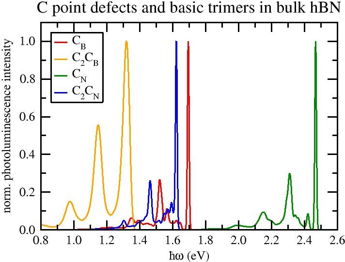
With up to three adjacent carbon atoms there are six basic ways to construct a paramagnetic defect (complex) exhibiting paramagnetic states: two neutral isolated point defects (C, C), two singly charged dimers (CC(+), CC(-)) and two neutral trimers (C2C, C2C) (cf. Figs. 1, 2, and 4, respectively). Starting from the CC dimer structures with larger separation between the point defects are also investigated. These are called “donor-acceptor pairs” (DAPs), because for the neutral case an electron transfer resulting in a non-paramagnetic structure (C and C) is energetically favorable (see the text below as well as Secs. III.1 and III.2). The DAPs are labeled according to their separation in the ideal lattice with “1” being the dimer. The five smallest separations are 1, 2, , , 4 (cf. Figs. 2, 3).
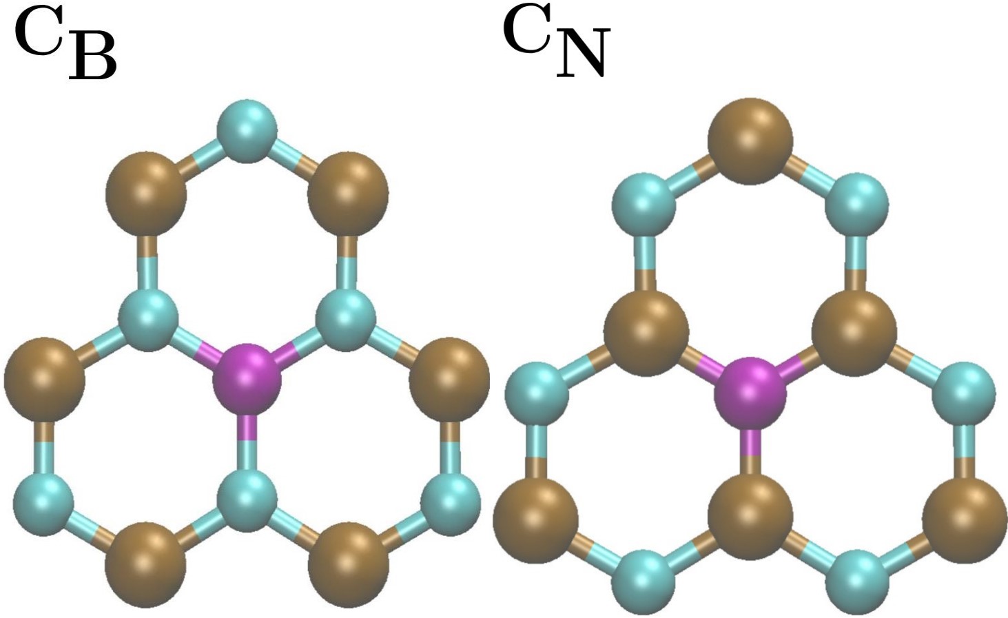
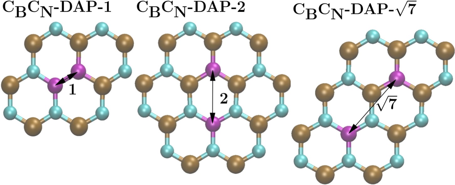
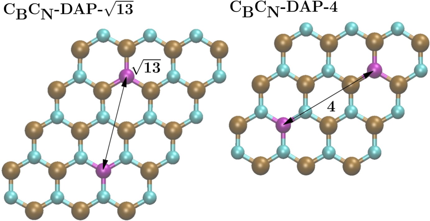
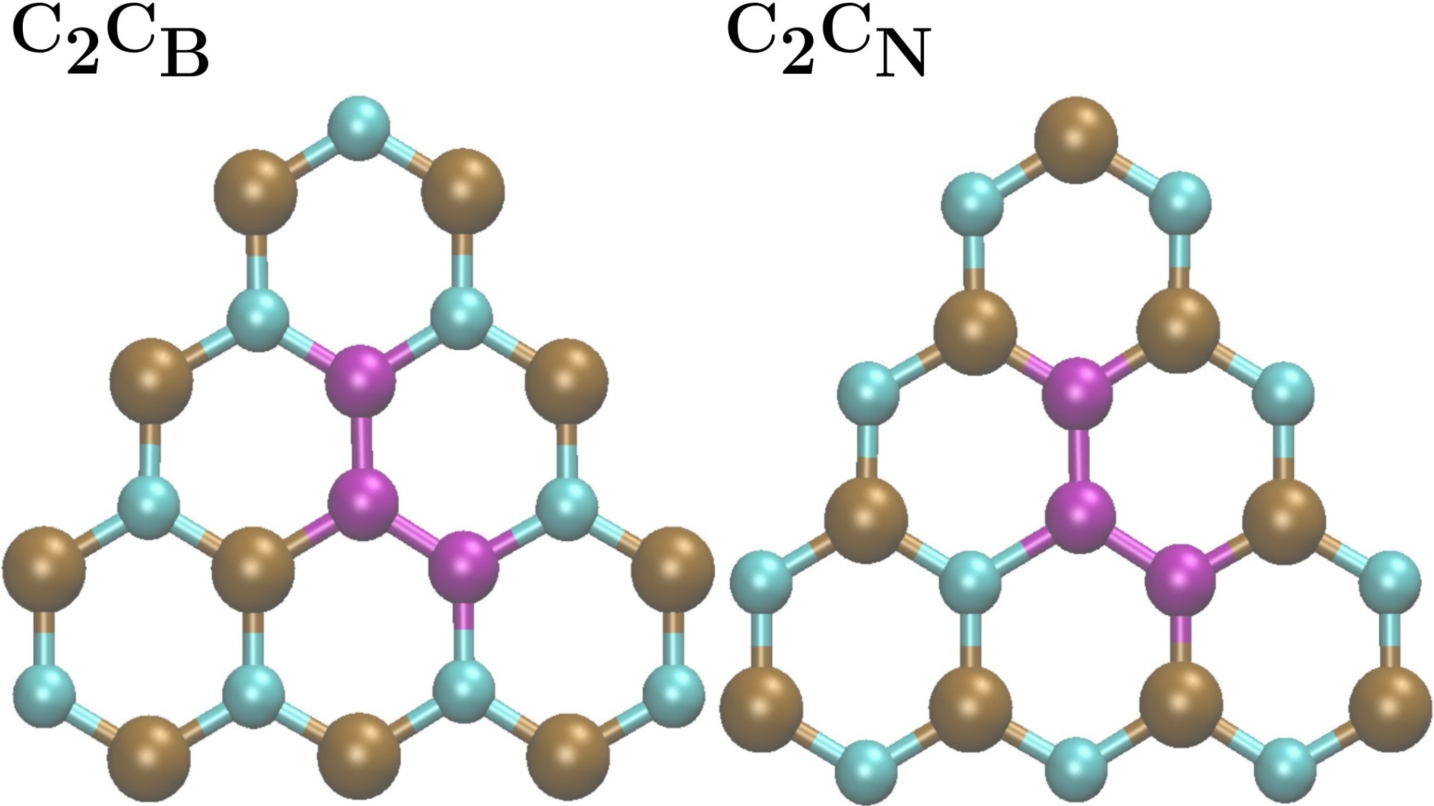
We plot the in-gap Kohn-Sham levels of the neutral defects in Fig. 5. The isolated neutral C and C defects introduce a single defect level into the fundamental band gap occupied by a single electron. The occupied level of C lies at higher energy than the empty level of C, thus the electron transfer occurs from C towards C when the defects are relatively close to each forming DAP complexes as noted above. This reflects in the calculated defect levels of DAP defects which show a completely filled low-energy level (localized around C) and an empty high-energy level (localized around C). By combining three carbon defects, i.e., the considered trimer complexes in our study, the electronic structure shows the characteristic of the constituent defects. In CC-trimer, two low-energy defect levels appear localized around C atoms and a high-energy level localized around C atom where the two low-energy defect levels are occupied by three electrons. In CC-trimer, rather one low-energy defect level and two high-energy defect levels appear in the gap occupied by three electrons.

The calculated binding energies are listed in Table 1. The donor-acceptor pairs are stabilized through charge transfer from C donor to C acceptor which involves Coulomb-interaction. As the attractive Coulomb-interaction increases with shorter distances the binding between C and C is stronger for pairs with shorter distances. The calculated binding energies clearly show this trend. We note that this looks to hold for the immediate C-C dimer defect but a C-C bond is created in that defect, and it cannot be described by the simple donor-acceptor pair model. Since the isolated carbon impurities introduce defect wavefunctions localized inside the host sheet and interlayer diffusion of carriers is hindered in hBN, complexes of carbon substitutional defects within a single sheet of hBN layer are considered in which we expect direct electron transfer between the constituting carbon defects. Certainly, different configurations of DAP and trimer complexes may occur in each hBN layer in multilayered hBN but we do not expect direct interaction between carbon defects residing in different layers of hBN.
| Defect | Binding energy (eV) |
|---|---|
| CC-DAPs | |
| 1 | -3.93 |
| 2 | -2.04 |
| -1.90 | |
| -1.52 | |
| 4 | -1.49 |
| trimers | |
| C2C | -5.31 |
| C2C | -5.28 |
III.1 Photoluminescence
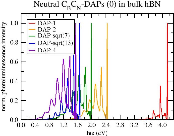
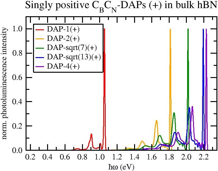
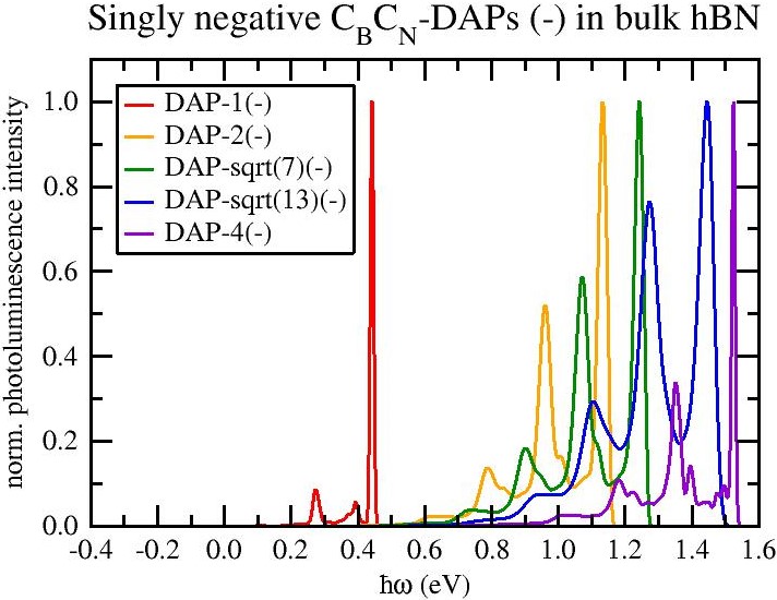
The ZPL energy is the first criterion for potentially identifying an experimentally isolated emitter. It has been calculated for all neutral systems and additionally also for the singly charged DAPs (cf. Tab. 2). The theoretical values range from 0.44 eV to 4.13 eV. depends on the electronic structure of the defect (complex), in particular its states inside the band gap, and its ionic relaxation triggered via deexcitation resp. emission.
The first optical excitation of a neutral point defect either transfers the unpaired electron from the band gap to the conduction band minimum (C, =1.695 eV, cf. Fig. 2) or instead transfers another electron from the valence band maximum into its orbital (C, =2.468 eV, cf. Fig. 2). The former electron transfer is within the majority spin channel, while it is the minority spin channel for the latter. This behavior was obtained earlier by Jara et al. [1], but they gave no values for .
Although the neutral point defects (C, C) are paramagnetic, their interaction leads to non-paramagnetic structures (CC-DAPs with “charge structure” C-C), because transferring the unpaired electron from C to C is energetically favorable. The CTLs C(+10) and C(0-1) (cf. Tab. 3) explain this for the limiting case of large separations. All numerical calculations at finite separations yielded the same behavior. Each CC-DAP exhibits two orbitals inside the band gap. The lower one is fully occupied and localized at C, while the higher one is empty and localized at C. The energy difference between them diminishes with increasing separation corroborating the results of Linderälv et al. [8].
of the neutral CC-DAPs diminishes with separation (cf. Tab. 2) as expected in view of the previous findings. The neutral CC dimer has been proposed to explain the ubiquitous 4.1-eV photoluminescence [9]. The calculated =4.13 eV is consistent with that and agrees well with the hybrid DFT (HSE) results of Mackoit-Sinkevičienė et al. (4.31 eV in Ref. 9), who also employed a bulk model, and Jara et al. (4.12 eV in Ref. 1), who employed a single layer model instead. On the contrary the underlying gradient DFT (PBE) is not sufficient to reproduce this result as found by Linderälv et al. (3.34 eV in Ref. 8).
The “charge structure” of the neutral CC-DAPs is C-C. Hence a singly charged DAP can be created either by removing the excess electron from C (positive DAP, C-C) or by adding an electron to C (negative DAP, C-C). In both cases the unpaired electron is localized at one point defect and the excess charge at the other one.
of both singly charged CC-DAPs increases with separation (cf. Tab. 2). It seems to approach a value equal, or at least similar, to that of the respective isolated neutral (paramagnetic) point defect. This convergence behavior had to be expected, because it turned out that the lowest optical excitation is linked to the same electronic transition as for the isolated neutral point defect. Hence the influence of the charged (non-paramagnetic) point defect vanishes with separation. The aforementioned Jara et al. [1] also found that of the singly charged dimers is too low for the visible range.
Placing a point defect (C or C) adjacent to the dimer (CC, abbreviated as C2) creates a basic trimer (C2C or C2C with the desired paramagnetic ground state, cf. Fig. 4). of the neutral basic trimers (1.36 eV for C2C, 1.62 eV for C2C) is lower than that of their neutral “building blocks” point defect and dimer (cf. Tab. 2). This is essentially due to the (overlap of) additional states inside the band. Jara et al. [1] obtained a similar value for C2C (1.62 eV), but a clearly higher one for C2C (1.65 eV). The origin of the discrepancy in the latter is unclear.
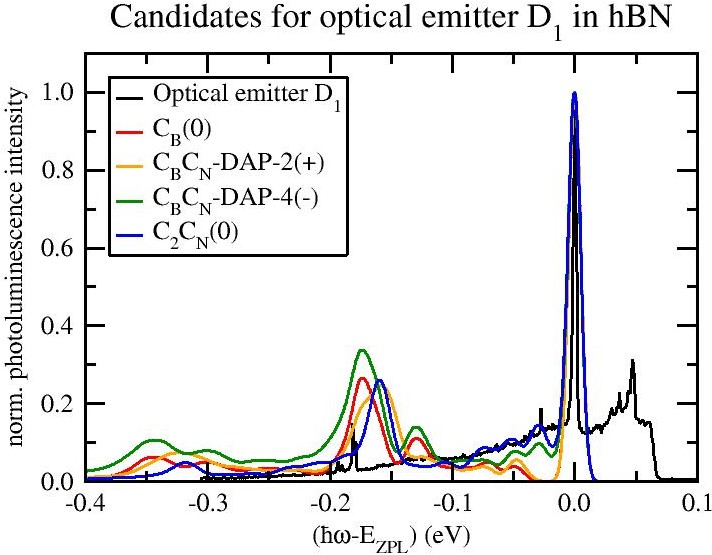
Beside the characteristic ZPL emission line (cf. Figs. 6, 7, 8, and 9), the most intense feature in the phonon sideband (PSB) always exhibited an energy detuning of 0.15-0.17 eV with respect to ZPL peak, except for the neutral dimer (0.20 eV). The intensity of its replica decreases with the number of quanta. Linderälv et al. [8] obtained similar results including a mostly somewhat larger PSB energy detuning of 0.18-0.20 eV for the neutral points defects and DAPs. According to them, these phonons are slightly distorted high-frequency in-plane modes of the ideal lattice, which would be at 0.15 eV, with the only exception (local mode) being the dimer (C-C bond). The present results are corroborated by Jara et al. [1], who report 0.20 eV resp. 0.16 eV for neutral CC resp. C2C and ascribe both to a local vibration mode. They also mention values in the same range for other substitutional carbon defects. Experimental PL spectra with similar features have been recorded by various groups [12, 7, 41, 6]. E.g. Mendelson et al. [7] recently observed several emitters with =2.08-2.16 eV and 0.16-0.20 eV PSB energy detuning upon illumination by 532-nm (2.33-eV) laser. The characteristics of the ODMR spin readout are in line with those found in a previous report [12] giving evidences for their connection to carbon-related defects although using a longer excitation wavelength (at least 594 nm or 2.09 eV) insufficient for exciting all of these emitters. Hence the singly positive CC-DAPs at larger separations (at least , cf. Tab. 2) may explain the observations if the defect ground state spin is .
Fig. 10 compares the PSBs of optical emitter D1, which was experimentally isolated by Chejanovsky et al. [12], to those of the candidates for its identification. D1 has =1.71 eV with a very similar PSB to the calculated ones and is paramagnetic with half-integer spin. We note that the other reported single photon emitters with longer wavelength ZPLs than that of 1.71-eV D1 center in Ref. 12 have different PL lineshape, so the characteristic PSBs are distinct from that of D1. On the other hand, all the considered carbon substitutional defects have very similar PSB features. Thus our paper now focuses on the identification of D1 center and it is beyond the scope to identify the other single photon emitters.
An error of 0.2 eV was allowed to take any kind of inaccuracy into account when the D1 ZPL energy is compared to the calculated ZPL energies. Hence the present study provides four candidates: C(0), CC-DAP-2(+), CC-DAP-4(-), C2C(0) (cf. Tab. 2). We note that we often anticipate an accuracy of about 0.1 eV for the calculated ZPLs. Here we expect a larger error for some of the considered defects as excitation to band edges is involved in the excited state which is a subject of finite size error for the neutral defects. Tests on C defect shows that the calculated increases by about 0.12 eV going from to supercell. Nevertheless, we provide the calculated ZPL energies within meV throughout the paper which is technically convergent in terms of the given supercell size () and DFT functional.
| Defect | (eV) | ||
|---|---|---|---|
| C() | 1.695 | ||
| C() | 2.468 | ||
| CC-DAPs | () | () | () |
| 4 | 2.229 | 1.547 | 1.525 |
| 2.194 | 1.655 | 1.446 | |
| 2.018 | 1.984 | 1.243 | |
| 2 | 1.814 | 2.432 | 1.133 |
| 1 (dimer) | 1.055 | 4.131 | 0.442 |
| Trimers | |||
| C2C() | 1.360 | ||
| C2C() | 1.623 | ||
| Emitter D1 | 1.710 | ||
III.2 Charge transition levels
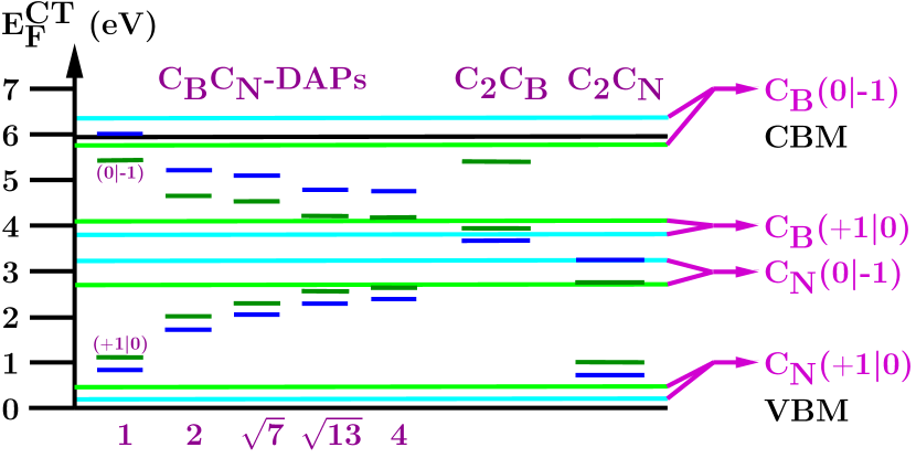
To modify the charge state of a specific defect it has to be understood how it depends on the Fermi level . The transition between two charge states happens at the CTL position where they are equally favorable. The defect charge can be modified accordingly if this transition is between the two most stable states and lies within the band gap.
The CTLs between neutral and singly charged ground states with respect to valence band maximum () are calculated as
| (2) |
where is the total energy of the defect with charge and is the charge correction. We note that we believe that the threedimensional model corresponds to the experimental conditions where the defects were found in multilayer hBN on a substrate which introduce a charge screening.
Tab. 3 summarizes the CTL positions. All uncorrected CTLs lie within the band gap as displayed in Fig. 11. C(+10) resp. C(0-1) is closest to the VBM resp. CBM. Since the charge structure of the neutral DAPs is C-C it is possible to either add an electron to C or to remove an electron from C in the presence of the other charged point defect. Hence CC(+10) resp. CC(0-1) converges to C(0-1) resp. C(+10) with increasing separation. Meanwhile CC(+10) is raised whereas CC(0-1) is lowered. This is not only due to the diminishing, and finally vanishing, stabilizing effect of the Coulomb interaction between the charged point defects on the neutral ground state (cf. Eq. (2)). It is also due to the decreasing energy difference between the orbitals involved in the charge transitions (highest occupied at C and lowest empty at C). As a consequence of this a “forbidden region” in which the Fermi level can be modified without affecting the charge of the point defects and DAPs exists between C(0-1) and C(+10). The CTLs have also been calculated for the basic trimers C2C and C2C. C2C(+10) and C2C(0-1) are similar to those of the isolated point defects without the “additional dimer” C2, whereas C2C(0-1) and C2C(+10) resemble those of C2.
The charge corrections stabilize the charged systems by several hundreds of meV (cf. Tab. 3) but the expected trend of convergence is not obvious for the corrected CTLs (cf. Fig. 11).
Note that similar values for the corrected CTL positions of point defects and dimer were found by Mackoit-Sinkevičienė et al. [9], while Weston et al. [2, 3] also give a similar value for C(+10) but a somewhat lower one for C(0-1). Just like in this work both employed a bulk model, hybrid DFT and charge corrections according to Freysoldt et al. [39, 40].
| Defect | CTL(+10) (eV) | CTL(0-1) (eV) |
|---|---|---|
| C | 3.81 (4.11) | 6.39 (5.79) |
| C | 0.21 (0.47) | 3.27 (2.72) |
| CC-DAPs | ||
| 1 | 0.85 (1.13) | 5.99 (5.42) |
| 2 | 1.73 (2.01) | 5.25 (4.68) |
| 2.02 (2.31) | 5.10 (4.53) | |
| 2.29 (2.57) | 4.81 (4.23) | |
| 4 | 2.37 (2.65) | 4.77 (4.20) |
| Trimers | ||
| C2C | 3.66 (3.94) | unclear (5.40) |
| C2C | 0.71 (0.98) | 3.29 (2.72) |
III.3 cw ODMR spectra
The cw ODMR spectrum, in particular the line shape resp. broadening, serves as a further criterion for identifying experimentally isolated emitters. It has been analyzed for all ground state systems (doublets), i.e. the neutral point defects and basic trimers as well as the singly charged DAPs (see also [17]).
The theoretical ODMR spectra are mostly obtained based on a simplified spin Hamiltonian taking into account the interaction of the unpaired electron with the external magnetic field B (electron Zeeman interaction ) and the spins of the nuclei (hyperfine interaction ). In the chosen approximation they are determined by the external magnetic field B (assuming a gyromagnetic tensor for the electron), the isotopic composition and the associated hyperfine matrices from hybrid DFT. The hyperfine parameters are calculated for the most abundant nuclear spin active isotopes (11B, 14N, 13C). Since nuclear spin active carbon is rare (13C of 1.1%), it is assumed that only boron (11B of 80.1%) and nitrogen (14N of 99.6%) contribute to the hyperfine splitting. For the neutral point defects and singly charged DAPs up to second neighbors (d=) of the paramagnetic carbon atom carrying the unpaired electron are taken into account. For the neutral basic trimers those of each carbon atom were chosen instead. The results and the justification of the underlying assumptions are discussed in the following.
We also considered a full spin Hamiltonian for test cases, e.g., C defect, which reads as
| (3) |
which includes nuclear Zeeman-term and nuclear quadrupole term too. The terms can be in Eq. (3) expressed as
| (4) |
where and are the Bohr-magneton of the electron and nuclei , and are the gyromagnetic factor and quadrupole moment of nuclei . In terms of broadening of the ESR signal, the most important parameter is the hyperfine tensor for nuclei . We will show that and can be typically neglected at non-zero magnetic fields, although, can contribute to the final shape of the ESR or ODMR spectrum coming from the 14N nuclei spins.
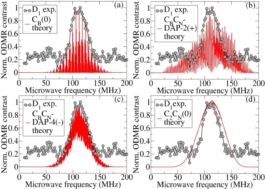
Tab. 4 summarizes the calculated line broadening and peak positions at an external magnetic field of 42 Gauss as used for the ODMR measurement of D1 spin center (cf. Fig. 12 and Ref. 12). The line broadening FWHM=2 is defined as the FWHM of a Gaussian normal distribution with the same standard deviation . The original peak position due to the electron Zeeman interaction is at 118 MHz (cf. Tab. 9). The asymmetric influence of the hyperfine interaction induces a defect-dependent blueshift of up to 15 MHz. Neutral C exhibits a much larger line broadening (74 MHz) than neutral C (43 MHz) as expected in view of the hyperfine constants (cf. Tabs. 5 and 6 and [17]). The underlying reason is that the gyromagnetic ratio of the boron isotope ( = 1366 Hz/Gauss for 11B), which is a first neighbor of the paramagnetic carbon for C but only a second neighbor for C, is more than four times larger than that of the nitrogen isotope ( = 308 Hz/Gauss for 14N). In view of the charge structure the line broadening of the singly positive resp. negative DAP has to converge to that of neutral C resp. C with increasing separation. While no unambiguous trend is found for the former, the presence of the charged point defect increases it for the latter. The line broadening of the basic trimers is smaller than that of the corresponding point defect without the adjacent dimer. We note that the C2C defect create a dense eigenvalue spectrum of the spin Hamiltonian with contribution of 14 nuclear spins which will result in a relatively smooth ODMR spectrum in the simulation.
| Defect type | FWHM (MHz) ( (MHz)) | |
|---|---|---|
| Point defects | C(0) | C(0) |
| 74 (132) | 43 (119) | |
| CC-DAPs | positive (+) | negative (-) |
| 4 | 74 (132) | 42 (119) |
| 73 (132) | 44 (119) | |
| 77 (133) | 49 (119) | |
| 2 | 71 (131) | 54 (119) |
| 1 (dimer) | 77 (125) | 70 (118) |
| Trimers | C2C(0) | C2C(0) |
| 51 (127) | 27 (119) | |
The experimental ODMR spectrum of D1 is compared to those calculated for the defect identification candidates C(0), CC-DAP-2(+), CC-DAP-4(-), C2C(0) (cf. Fig. 12). It is concluded that D1 has to be either C(0) or at least a very similar structure where the spin density is localized around C. As previously discussed the theoretical model fulfills the conditions found by Chejanovsky et al. [12] and all defect identification candidates exhibit PL in good agreement with the measured spectrum. However C(0) is the simplest and best explanation of the observed ODMR, while non-similar structures provide only inferior spectra. The observed ODMR peak is centered at 112-113 MHz. A constant shift of every single calculated spectrum has been introduced to match this value, since the magnetic field measurement (42 Gauss) may have an error of a few Gauss. For C(0) and CC-DAP-4() ( MHz) it is smaller than for C2C(0) ( MHz) and CC-DAP-2(+) ( MHz). While C(0) with 43 MHz line broadening yields a very good reproduction of the observed peak, the spectra of C2C(0) (51 MHz) and especially CC-DAP-2(+) (71 MHz) are clearly broader. In view of the charge structure the results for C(0) and CC-DAP-4() are close to each other. In both defects, the spin density is localized around C, so one can conclude that C defect should be involved in the D1 spin center.
Although the experimental background might reach up to 40% of the peak maximum, it can not lead to another interpretation of the results or a substantial reduction of their quality. The measured intensities within, and only within, the interval 92-134 MHz are 40% while they come close to this value at some other frequencies. It is hence an upper bound for the background. Since even after subtraction of the full 40% (as background correction) the normalized peak within the relevant interval is only slightly less broad, so the conclusions remain unchanged.
The hyperfine constants of C(0) are given in Tab. 5. Note that the involvement of nuclear spin active carbon ( = 1071 Hz/Gauss for 13C) would substantially split the ODMR peak of C(0) to a doublet because of the huge spin density on the carbon atom attributed to the unpaired electron localized on its orbital. This behavior is also found for the other defects [17]. Measuring it would provide further insight into the structure of D1 and/or other experimentally isolated emitters.
The hyperfine parameters include the contribution of the spin polarization of the core electrons to the Fermi contact interaction. Tab. 6 takes neutral C as an example to show that this contribution can be significant, in particular if the carbon is nuclear spin active. Without it Sajid et al. [4] found hyperfine constants in reasonable agreement employing a 2D model and the regular HSE06 functional. Our calculations imply that the core polarization should be included in the calculations of accurate hyperfine tensors.
| total | # | d(C) | (MHz) | (MHz) | (MHz) |
|---|---|---|---|---|---|
| C | 1 | 0 | 12.1 | 12.1 | 231.3 |
| N | 3 | 1 | -9.0 | -5.1 | -9.0 |
| B | 6 | 1.4 | -0.9 | 6.1 |
| total | # | d(C) | (MHz) | (MHz) | (MHz) | (MHz) |
|---|---|---|---|---|---|---|
| C | 1 | 0 | -19.2 (44.8) | -19.2 (44.8) | 156.5 (220.5) | -64.0 |
| B | 3 | 1 | -17.9 (-16.7) | -16.0 (-14.8) | -24.5 (-23.3) | -1.2 |
| N | 6 | -0.2 (0.8) | -0.8 (0.1) | 2.4 (3.4) | -1.0 |
The influence of the isotopic composition on the ODMR spectra of the point defects (see Tabs. 7 and 8) was analyzed, because 10B is also significantly abundant (19.9%). Replacing 11B with 10B gradually reduces the line broadening, because the hyperfine matrices scale linearly with the nuclear gyromagnetic factor (g = instead of ) although the nuclear spin is increased ( instead of ) [42]. This effect is more pronounced for neutral C, since the boron isotopes are first neighbors of the paramagnetic carbon. In this case it also affects the peak center which is slightly redshifted. Considering only 11B is usually a good approximation, since large changes of the ODMR spectra (dominant contribution of 10B) are unlikely to be observed at the natural distribution of isotopes.
| #(11B) | #(10B) | p(%) | (MHz) | FWHM (MHz) |
|---|---|---|---|---|
| 6 | 0 | 26.41 | 119 | 43 |
| 5 | 1 | 39.37 | 119 | 41 |
| 4 | 2 | 24.45 | 119 | 39 |
| 3 | 3 | 8.10 | 119 | 37 |
| 2 | 4 | 1.51 | 119 | 34 |
| 1 | 5 | 0.15 | 119 | 32 |
| 0 | 6 | 0.01 | 119 | 29 |
| #(11B) | #(10B) | p (%) | (MHz) | FWHM (MHz) |
|---|---|---|---|---|
| 3 | 0 | 51.39 | 132 | 74 |
| 2 | 1 | 38.30 | 129 | 66 |
| 1 | 2 | 9.52 | 126 | 57 |
| 0 | 3 | 0.79 | 123 | 45 |
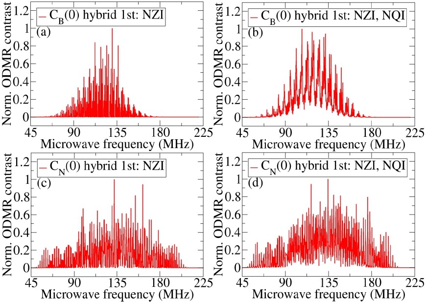
The peak broadening is essentially determined by the hyperfine interaction and the simplified spin Hamiltonian (evaluated with second-order perturbation theory) yields already a good approximation of the ODMR spectra. This is demonstrated using the most basic example of the neutral point defects C and C. However it has to be kept is mind that a comprehensive discussion of the full spin Hamiltonian is beyond the scope of the present study. Tab. 9 summarizes the results for line broadening and peak center position obtained from different approaches. Further simplifying the spin Hamiltonian via using only the hyperfine constants, instead of the full hyperfine tensor is not justified. It leads to a significant overestimation of the line broadening, in particular for C (38 MHz) whose peak center is additionally redshifted (5 MHz). Since second-order perturbation theory cannot be combined with exact diagonalization for specific nuclei in the code, first-order perturbation theory is also considered. Since the C peak center is redshifted by 14 MHz, this seems to be a non-accurate approach. Exact diagonalization allows to include the nuclear Zeeman interaction and additionally the nuclear quadrupole interaction, which have an indirect effect on the electronic transitions as the HFI couples the electronic spin to the nuclear spins. Due to computational expense which scales exponentially with the number of spins in the Hilbert space it was performed only for the first (1st) neighbors of the respective point defect. Including the NZI reverses the 14 MHz redshift of the C peak center. However this might also be related to the underlying change of the algorithm to solve the spin Hamiltonian. Note that the NZI leads to core transition peaks in a low frequency range (30MHz) that was not included in the calculation of peak center and line broadening. Judging from Fig. 13 the NQI can still have a non-negligible effect on the spectral shape although peak center and line broadening are hardly affected (cf. Tab. 9). Indeed the entries of the matrices (cf. Eqs. (1) and (3) and [17]) are 1MHz. Hence the line splittings induced by the NQI can only be correspondingly small. However it can also induce significant intensity redistribution explaining its importance in the given context. The results for C are further evidence for its near-identification as experimentally isolated optical emitter D1.
| Approach | FWHM (MHz) ( (MHz)) | |
|---|---|---|
| C(0) | C(0) | |
| EZI only | 0 (118) | 0 (118) |
| perturb2 ( constants) | 112 (127) | 49 (119) |
| perturb2 (full ) | 74 (132) | 43 (119) |
| perturb1 (full ) | 73 (118) | 43 (118) |
| hybrid (1st: NZI) | 72 (132) | 42 (119) |
| hybrid (1st: NZI, NQI) | 72 (132) | 42 (119) |
III.4 Summary
Paramagnetic substitutional carbon defects in hexagonal boron nitride have been characterized via modeling their photoluminescence spectra, charge transition levels and cw ODMR spectra. Clear trends in all of these were found by analyzing the separation between C and C. Furthermore a near-identification of an experimentally isolated optical emitter D1 as neutral C is given.
=1.695 eV (2.468 eV) was obtained for neutral C (C) which are approximate values due to the finite size effects and the accuracy in the applied DFT functional. of the singly negative (positive) CC-DAP converges to this, or at least a similar, value from below with increasing separation. This behavior is explained based on the relevant electronic transition and the charge structure. The result for the neutral dimer (CC, =4.131 eV), which allegedly causes the ubiquitous 4.1-eV photoluminescence [9], is consistent with previous hybrid DFT results [9, 1]. of the neutral CC-DAPs has to decrease with separation due to the position of the states inside the band gap (see also [8]). Each basic trimer has a lower than its “building blocks” point defect and dimer as expected in view of the overlap of their states inside the band gap.
An intense feature in PSB next to ZPL at 0.15-0.17 eV (except for the neutral dimer at 0.20 eV) was found for all defects. Similar results were obtained in theoretical [1, 8] as well as experimental [12, 7, 41, 6] studies. In particular ODMR experiments yielded evidences for the connection of these features to carbon-related defects [7, 12]. Four candidates for the identification of D1 spin center were provided based on the agreement with the ZPL energies within 0.2 eV accuracy.
The cw ODMR spectra for all ground state systems have been calculated at 42 Gauss external magnetic field based on a simplified spin Hamiltonian. The asymmetric influence of the hyperfine interaction induces a defect-dependent blueshift of the peak positions from 118 MHz up to 133 MHz. C exhibits a much larger line broadening than C due to the hyperfine parameters. Replacing 11B with the less abundant 10B reduces the peak width and can also shift the peak center. However large changes are unlikely to be observed at the natural distribution of isotopes. The charge structure explains the convergence of the line broadening of the singly charged CC-DAPs.
The calculated ZPL energy and PSB as well as the ESR spectrum strongly implies that C is involved as spin-active part of the D1 spin center, and it could be the isolated neutral C defect. Measuring the ODMR splitting due to 13C isotope would provide further insight about the chemical composition of D1 or other emitters.
An exemplary analysis of the point defects demonstrates that the ODMR line broadening is essentially due to hyperfine interaction. The simplified spin Hamiltonian together with second-order perturbation theory results in a good approximation of the spectra. Using only the hyperfine constants, i.e. neglecting the Euler angles, is not appropriate as it leads to a large overestimation of the line broadening. A hybrid approach allowed to include the nuclear Zeeman and additionally the quadrupole interaction for the first neighbors. The line broadening remained essentially unaffected. Nuclear quadrupole interaction is important for an exact description of the spectral shape as it can lead to non-negligible modifications of the intensities but it does not effect the overall broadening of the ESR signal.
IV Conclusions and outlook
The modeling of PL and ODMR spectra has yielded helpful criteria for the identification of paramagnetic substitutional carbon defects in hBN. An example for a near-identification as neutral C has been given. The separation between C and C emerged as key to control the ZPL wavelength and charge compensation of defects. All findings are further steps towards the identification of these structures and later their target-oriented engineering as quantum bits.
It is demonstrated that first principles theory is able to predict the complex electron spin resonance spectrum of defects in hBN. It has been found that the full hyperfine tensor of the nuclei is required to accurately determine the linewidth and the central position of the ODMR signal at a given external magnetic fields. As direct measurement of the full hyperfine tensors is challenging our results demonstrate that the accurate interpretation of ESR and ODMR signals in hBN requires a tight cooperation between experimental and ab initio theoretical spectroscopy.
Acknowledgements
We are grateful to Prof. Jörg Wrachtrup and Dr. Durga Dasari for sharing and explaining their experimental results, Christoph Freysoldt for discussions about his charge correction scheme and EasySpin creator Stefan Stoll for helping us to use his program. This research was supported by the Ministry of Innovation and Technology and the National Research, Development and Innovation Office (NKFIH) within the Quantum Information National Laboratory of Hungary, the National Quantum Technology Program (NKFIH Grant No. 2017-1.2.1-NKP-2017-00001), the National Excellence Program (NKFIH Grant No. KKP129866), as well as the support of European Commission within the Quantum Technology Flagship Project ASTERIQS (Grant No. 820394). We acknowledge that the results of this research have been achieved using the DECI resource Eagle HPC based in Poland at Poznan with support from the PRACE aisbl and resources provided by the Hungarian Governmental Information Technology Development Agency, including the project “gallium”.
References
- Jara et al. [2021] C. Jara, T. Rauch, S. Botti, M. A. L. Marques, A. Norambuena, R. Coto, J. E. Castellanos-Águila, J. R. Maze, and F. Munoz, First-principles identification of single photon emitters based on carbon clusters in hexagonal boron nitride, J. Phys. Chem. A 125, 1325 (2021).
- Weston et al. [2018] L. Weston, D. Wickramaratne, M. Mackoit, A. Alkauskas, and C. G. V. de Walle, Native point defects and impurities in hexagonal boron nitride, Phys. Rev. B 97, 214104 (13) (2018).
- Weston et al. [2020] L. Weston, D. Wickramaratne, M. Mackoit, A. Alkauskas, and C. G. V. de Walle, Erratum: Native point defects and impurities in hexagonal boron nitride [phys. rev. b 97, 214104 (2018)], Phys. Rev. B 102, 099903 (2) (2020).
- Sajid et al. [2018] A. Sajid, J. R. Reimers, and M. J. Ford, Defect states in hexagonal boron nitride: Assignments of observed properties and prediction of properties relevant to quantum computation, Phys. Rev. B 97, 064101 (9) (2018).
- Hayee et al. [2020] F. Hayee, L. Yu, J. L. Zhang, C. J. Ciccarino, M. Nguyen, A. F. Marshall, I. Aharonovich, J. Vučković, P. Narang, T. F. Heinz, and J. A. Dionne, Revealing multiple classes of stable quantum emitters in hexagonal boron nitride with correlated optical and electron microscopy, Nat. Mater. 19, 534 (2020).
- Bourrellier et al. [2016] R. Bourrellier, S. Meuret, A. Tararan, O. Stéphan, M. Kociak, L. H. G. Tizei, and A. Zobelli, Bright uv single photon emission at point defects in h-bn, Nano Lett. 16, 4317 (2016).
- Mendelson et al. [2021] N. Mendelson, D. Chugh, J. R. Reimers, T. S. Cheng, A. Gottscholl, H. Long, C. J. Mellor, A. Zettl, V. Dyakonov, P. H. Beton, S. V. Novikov, C. Jagadish, H. H. Tan, M. J. Ford, M. Toth, C. Bradac, and I. Aharonovich, Identifying carbon as the source of visible single-photon emission from hexagonal boron nitride, Nat. Mater. 20, 321 (2021).
- Linderälv et al. [2021] C. Linderälv, W. Wieczorek, and P. Erhart, Vibrational signatures for the identification of single-photon emitters in hexagonal boron nitride, Phys. Rev. B 103, 115421 (13) (2021).
- Mackoit-Sinkevičienė et al. [2019] M. Mackoit-Sinkevičienė, M. Maciaszek, C. G. V. de Walle, and A. Alkauskas, Carbon dimer defect as a source of the 4.1 ev luminescence in hexagonal boron nitride, Appl. Phys. Lett. 115, 212101 (4) (2019).
- Korneychuk et al. [2018] S. Korneychuk, G. Guzzinati, and J. Verbeeck, Measurement of the indirect band gap of diamond with eels in stem, Phys. Status Solidi A 215, 1800318 (7) (2018).
- Cassabois et al. [2016] G. Cassabois, P. Valvin, and B. Gil, Hexagonal boron nitride is an indirect bandgap semiconductor, Nat. Photonics 10, 262 (2016).
- Chejanovsky et al. [2021] N. Chejanovsky, A. Mukherjee, J. Geng, Y.-C. Chen, Y. Kim, A. Denisenko, A. Finkler, T. Taniguchi, K. Watanabe, D. B. R. Dasari, P. Auburger, A. Gali, J. H. Smet, and J. Wrachtrup, Single-spin resonance in a van der waals embedded paramagnetic defect, Nat. Mater. 10.1038/s41563-021-00979-4 (2021).
- Gottscholl et al. [2020] A. Gottscholl, M. Kianinia, V. Soltamov, S. Orlinskii, G. Mamin, C. Bradac, C. Kasper, K. Krambrock, A. Sperlich, M. Toth, I. Aharonovich, and V. Dyakonov, Initialization and read-out of intrinsic spin defects in a van der Waals crystal at room temperature, Nat. Mater. 19, 540 (2020).
- Ivády et al. [2020] V. Ivády, G. Barcza, G. Thiering, S. Li, H. Hamdi, J.-P. Chou, O. Legeza, and A. Gali, Ab initio theory of the negatively charged boron vacancy qubit in hexagonal boron nitride, npj Comp. Mat. 6, 1 (2020).
- Sajid et al. [2020] A. Sajid, K. S. Thygesen, J. R. Reimers, and M. J. Ford, Edge effects on optically detected magnetic resonance of vacancy defects in hexagonal boron nitride, Communications Physics 3, 1 (2020).
- Abdi et al. [2018] M. Abdi, J.-P. Chou, A. Gali, and M. B. Plenio, Color Centers in Hexagonal Boron Nitride Monolayers: A Group Theory and Ab Initio Analysis, ACS Photonics 5, 1967 (2018).
- [17] See the Supplemental Material at … to be provided by the editor … for a collection of data regarding hyperfine coupling and electronic electric field gradients (EFGs) at the atomic nuclei. The data for the full matrices can be made available upon request.
- Kresse and Furthmüller [1996] G. Kresse and J. Furthmüller, Efficient iterative schemes for ab initio total-energy calculations using a plane-wave basis set, Phys. Rev. B. 54, 11169 (18) (1996).
- Kresse and Joubert [1999] G. Kresse and D. Joubert, From ultrasoft pseudopotentials to the projector augmented-wave method, Phys. Rev. B 59, 1758 (1999).
- Heyd et al. [2003] J. Heyd, G. E. Scuseria, and M. Ernzerhof, Hybrid functionals based on a screened coulomb potential, J. Chem. Phys. 118, 8207 (2003).
- Heyd et al. [2006] J. Heyd, G. E. Scuseria, and M. Ernzerhof, Erratum: Hybrid functionals based on a screened coulomb potential [j. chem. phys. 118, 8207 (2003)], J. Chem. Phys. 124, 219906 (1) (2006).
- Doan et al. [2016] T. C. Doan, J. Li, J. Y. Lin, and H. X. Jiang, Bandgap and exciton binding energies of hexagonal boron nitride probed by photocurrent excitation spectroscopy, Appl. Phys. Lett. 109, 122101 (5) (2016).
- Perdew et al. [1996] J. P. Perdew, K. Burke, and M. Ernzerhof, Generalized gradient approximation made simple, Phys. Rev. Lett. 77, 3865 (1996).
- Perdew et al. [1997] J. P. Perdew, K. Burke, and M. Ernzerhof, Erratum: Generalized gradient approximation made simple [phys. rev. lett. 77, 3865 (1996)], Phys. Rev. Lett. 78, 1396 (1997).
- Paszkowicz et al. [2002] W. Paszkowicz, J. B. Pelka, M. Knapp, T. Szyszko, and S. Podsiadlo, Lattice parameters and anisotropic thermal expansion of hexagonal boron nitride in the 10–297.5k temperature range, Appl. Phys. A 75, 431 (2002).
- Grimme et al. [2010] S. Grimme, J. Antony, S. Ehrlich, and H. Krieg, A consistent and accurate ab initio parametrization of density functional dispersion correction (dft-d) for the 94 elements h-pu, J. Chem. Phys. 132, 154104 (19) (2010).
- Smith et al. [2016] D. G. A. Smith, L. A. Burns, K. Patkowski, and C. D. Sherrill, Revised damping parameters for the d3 dispersion correction to density functional theory, J. Phys. Chem. Lett. 7, 2197 (2016).
- Grimme et al. [2011] S. Grimme, S. Ehrlich, and L. Goerigk, Effect of the damping function in dispersion corrected density functional theory, J. Comput. Chem. 32, 1456 (2011).
- Alkauskas et al. [2014] A. Alkauskas, B. B. Buckley, D. D. Awschalom, and C. G. V. de Walle, First-principles theory of the luminescence lineshape for the triplet transition in diamond nv centres, New J. Phys. 16, 073026 (23) (2014).
- Gali et al. [2009] A. Gali, E. Janzén, P. Deák, G. Kresse, and E. Kaxiras, Theory of Spin-Conserving Excitation of the $N\ensuremath{-}{V}^{\ensuremath{-}}$ Center in Diamond, Physical Review Letters 103, 186404 (2009).
- Attaccalite et al. [2011] C. Attaccalite, M. Bockstedte, A. Marini, A. Rubio, and L. Wirtz, Coupling of excitons and defect states in boron-nitride nanostructures, Phys. Rev. B 83, 144115 (2011).
- Blöchl [2000] P. E. Blöchl, First-principles calculations of defects in oxygen-deficient silica exposed to hydrogen, Phys. Rev. B 62, 6158 (2000).
- Szász et al. [2013] K. Szász, T. Hornos, M. Marsman, and A. Gali, Hyperfine coupling of point defects in semiconductors by hybrid density functional calculations: The role of core spin polarization, Phys. Rev. B 88, 075202 (7) (2013).
- Stoll [2003] S. Stoll, Spectral simulations in solid-state electron paramagnetic resonance, (phd) dissertation, ETH Zürich (2003).
- Stoll and Schweiger [2006] S. Stoll and A. Schweiger, Easyspin, a comprehensive software package for spectral simulation and analysis in epr, J. Magn. Reson. 178, 42 (2006).
- Stoll [2015] S. Stoll, Chapter six - cw-epr spectral simulations: Solid state, in Electron Paramagnetic Resonance Investigations of Biological Systems by Using Spin Labels, Spin Probes, and Intrinsic Metal Ions, Part A, Methods in Enzymology, Vol. 563, edited by P. Z. Qin and K. Warncke (Academic Press, 2015) pp. 121–142.
- Petrilli et al. [1998] H. M. Petrilli, P. E. Blöchl, P. Blaha, and K. Schwarz, Electric-field-gradient calculations using the projector augmented wave method, Phys. Rev. B 57, 14690 (1998).
- Stoll and Goldfarb [2017] S. Stoll and D. Goldfarb, Epr interactions – nuclear quadrupole couplings, in eMagRes, Vol. 6 (American Cancer Society, 2017) pp. 495–510, https://onlinelibrary.wiley.com/doi/pdf/10.1002/9780470034590.emrstm1504 .
- Freysoldt et al. [2011] C. Freysoldt, J. Neugebauer, and C. G. V. de Walle, Electrostatic interactions between charged defects in supercells, Phys. Stat. Sol. B 248, 1067 (2011).
- Freysoldt et al. [2009] C. Freysoldt, J. Neugebauer, and C. G. V. de Walle, Fully Ab Initio finite-size corrections for charged-defect supercell calculations, Phys. Rev. Lett. 102, 016402 (4) (2009).
- Museur et al. [2008] L. Museur, E. Feldbach, and A. Kanaev, Defect-related photoluminescence of hexagonal boron nitride, Phys. Rev. B 78, 155204 (8) (2008).
- [42] At this point the order of replacement is irrelevant in view of the nuclear symmetry and the neglect of core-core interaction in the spin Hamiltonian.