A compact linear accelerator based on a scalable microelectromechanical-system RF-structure
Abstract
A new approach for a compact radio-frequency (RF) accelerator structure is presented. The new accelerator architecture is based on the Multiple Electrostatic Quadrupole Array Linear Accelerator (MEQALAC) structure that was first developed in the 1980s. The MEQALAC utilized RF resonators producing the accelerating fields and providing for higher beam currents through parallel beamlets focused using arrays of electrostatic quadrupoles (ESQs). While the early work obtained ESQs with lateral dimensions on the order of a few centimeters, using printed circuits board (PCB), we reduce the characteristic dimension to the millimeter regime, while massively scaling up the potential number of parallel beamlets. Using Microelectromechanical systems scalable fabrication approaches, we are working on further reducing the characteristic dimension to the sub-millimeter regime. The technology is based on RF-acceleration components and ESQs implemented in PCB or silicon wafers where each beamlet passes through beam apertures in the wafer. The complete accelerator is then assembled by stacking these wafers. This approach has the potential for fast and inexpensive batch fabrication of the components and flexibility in system design for application specific beam energies and currents. For prototyping the accelerator architecture, the components have been fabricated using PCB. In this paper, we present proof of concept results of the principal components using PCB: RF acceleration and ESQ focusing. Ongoing developments on implementing components in silicon and scaling of the accelerator technology to high currents and beam energies are discussed.
pacs:
29.20.-c,29.27.-a,41.75.-,41.85.Ne, 07.77.KaI Introduction
Ion beams have many applications in research and industry. Increasing intensity and reducing the size and cost are important aspects of developing new particle accelerators for many possible applications.
Among them the most ambitious applications for high-intensity beams are driving nuclear fusion power systems for the purpose of electricity generation. At present, there are two main approaches to achieving practical fusion energy production, magnetic fusion energy (MFE) and inertial fusion energy (IFE). In both approaches, high intensity particle beams have been proposed as methods to heat the fusion fuel.
In MFE, typified by toroidal devices called tokamaks, magnetically confined deuterium and tritium plasma would be heated to fusion conditions, i.e., an ion temperature of , at least in part, by intense 0.1-1.0 MeV neutral deuterium beams in order to initiate fusion reactions. In principle, the resulting charged reaction product, the 3.5 MeV helium nucleus, will be able to maintain the plasma temperature above 10 keV indefinitely in a well designed magnetic confinement system. The International Thermonuclear Experimental Reactor (ITER), now under construction in France,Takatsu (2011) will have two 16.5 MW deuterium beam systems with negative ions accelerated to 1 MeV kinetic energy before being neutralized and injected into the device. Each beamline occupies a volume exceeding .Hemsworth et al. (2009)
The idea of using ion beam accelerators for IFE arose in the 1970’s shortly after the recognition that lasers might drive inertial fusion targets.Nuckolls et al. (1972) In laser and ion beam driven targets, the fuel is a spherical shell a few millimeters in diameter. Ion beam energy of the order of 1-10 MJ must be delivered in to achieve fusion ignition, and computer simulations indicate that more energy may be created from the fusion reactions before the compressed fuel disassembles.Bangerter, Faltens, and Seidl (2013) In contrast to the magnetic fusion approach, the process here is pulsed, with a repetition rate of several Hertz. The ion beam requirements are constrained by the target design: for heavy ions, , a kinetic energy of several GeV and currents in the kiloampere range are required; for lighter ions and the same total beam energy, since the MeV per nucleon must be similar, the current must be increased appropriately.
There is also interest in magneto-inertial fusion (MIF), where aspects of magnetic and inertial fusion approaches are merged. Initially low density deuterium-tritium plasma is confined by a magnetic field. The plasma and embedded magnetic field are compressed by, e.g., a metal liner, directed plasma or beams, with a confinement time longer than characteristic of IFE and shorter than MFE.Lindemuth and Siemon (2009); Wurden et al. (2016)
For the IFE and MIF fusion energy applications, the required total energy per pulse . For example, consider indirect drive IFE driven with 5 MJ pulses of 5 GeV heavy ions in a 10 ns pulse. The corresponding total beam current is and is distributed among approximately 100 beams. With present-day accelerator technology, the accelerators generating the fusion driver beams would be kilometers long and are usually the most costly aspects of the fusion energy power plant system. For MIF systems, the final beam pulse duration is longer, (), while the desired ion energy is typically lower (). Thus, the required current could be higher depending on the drive pulse duration which can vary widely from the nanoseconds timescale to hundreds of microseconds.Wurden et al. (2016)
Most ion accelerators have average acceleration gradients of 1-5 over their length. Comprising focusing magnets and acceleration cells (radio-frequency or induction accelerators), they have transverse dimensions approximately 0.1-0.5 m, not including power supplies, vacuum pumps, and other ancillary equipment. For non-fusion applications, the beam requirements tend to be less demanding. Nevertheless, the state-of-the-art accelerator architectures in these applications have similar footprint and cost.
This work is motivated by the use of microfabrication based approaches to both miniaturize and reduce system cost. Applying fabrication approaches widely used to fabricate Microelectromechanical systems (MEMS), waferscale fabrication has the potential of reducing cost and increasing performance.Shi and Lal (2011) In particular, fabrication of small orifices in the millimeter range with submicron lithography enables high precision and high electric fields at modest voltages. In order to generate high power beams, we propose to accelerate many parallel beams in a common accelerator structure and vacuum system. Utilizing MEMS technology, the beamlets can be densely packed, leading to a lower-cost and reliable accelerator architecture for the applications above.
The idea of a scaled down high energy physics accelerator architecture was presented by Maschke,Maschke (1979) motivated by the need to generate high current and brightness beams for ion-driven IFE. He proposed a Multiple Electrostatic Quadrupole Array Linear Accelerator (MEQALAC) structure consisting of electrostatic quadrupoles (ESQs) and radio-frequency (RF) acceleration. The current limit for an ESQ focusing lattice is given by
| (1) |
where is the beam aperture (distance to the focusing electrode pole tip), the maximum electric field, and the ion beam velocity.Hogan, Bangerter, and Kulcinski (1992); Faltens and Seidl (1996) The peak electric field is bound by the breakdown field of the quadrupole structure. Measured breakdown fields stay constant or increase when scaling down the gap distance.Slade and Taylor (2002); Faltens and Seidl (1996) The current density averaged over the focusing structure increases inversely with and the total current can be increased by accelerating and focusing multiple closely-packed beamlets in separate focusing channels. Although magnetic quadrupoles offer stronger focusing than ESQs at higher beam velocities, they do not scale well to smaller sizes, i.e., the current density needed to create the magnetic field increases when scaling down the quadrupole size. In practice, the smallest useful size for the quadrupole structures will be limited by alignment and fabrication errors of the structure. MEMS technology pushes the boundaries of these fabrication errors into the sub-micrometer range and, therefore, allows drastic improvements in transportable currents. In fact, the theoretical current density transport limits achievable with an aperture of the order of , a unit cell size of , and an applied field of (taken as 50% of the breakdown limit from Fig. 4 in Ref. 11) will be for Xe ions and for H ions, both at 10 keV. Normal ion sources produce of the order of beam currents for Xe. For hydrogen, has been achieved.Skalyga et al. (2016) The ion source will therefore be the limiting factor in most applications, and bunching, funneling, or other methods of increasing the current density might be utilized to overcome this limitation.
II Concept
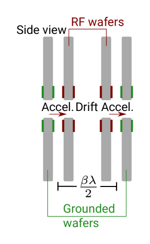
The proposed accelerator structure consists of two main components: RF units and ESQ doublets. The RF units will provide the acceleration for the ion beam bunches, and the ESQs will provide transverse focusing along the accelerator structure. Each RF unit consists of two vacuum gaps between ring electrodes that define acceleration and field-free drift regions. The field-free drift gap is set so that
| (2) |
where is the RF wavelength and , and is the center-to-center distance between adjacent acceleration gaps. Successive gaps can easily take into account the increasing particle due to acceleration. Thus particles see nearly identical acceleration fields in adjacent gaps since the RF phase advances by (see Fig. 1(a)). For each RF unit, the ion bunches enter and leave the unit at ground potential. Components consist of either silicon wafers or printed circuit boards (PCB). For this paper, we will refer to both as wafers independent of the chosen implementation. All RF wafers share the same design making batch fabrication possible: each beamlet corresponds to a through hole aperture in the wafer that has a ring electrode at its entrance and exit on the surface of the wafer. In silicon, this would be a deposited metal ring, and in our PCB implementation, the on-board copper is utilized for this purpose. To create an RF unit, four wafers are stacked together. Both sides of the outer wafers are grounded and the four sides of the inner wafers are connected to a common RF source (see Fig. 1(a)). We have chosen acceleration gaps of 1.4 mm for the experiments reported here. Precision washers are used between the wafers to define the gap distances.
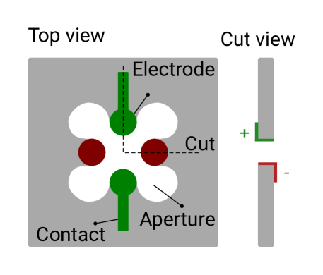
For transverse focusing, each ESQ consists of two pairs of electrodes which are biased to . To implement ESQ components, we form four electrodes around each beam aperture with electrical connections to the front and back of each wafer for the positive and negative voltages (see Fig. 1(b)). The ESQ structure is therefore completely contained in a single wafer. A single ESQ wafer focuses the beam in one direction and defocuses the beam in the other. We therefore use two ESQ wafers to form a focusing doublet to provide an overall focusing effect on the beam.
III Fabrication
For initial proof-of-concept experiments, we utilize FR-4 PCB to fabricate the RF and ESQ wafers. We are also exploring the fabrication of quadrupole structures using 3D-printing techniques as well as quadrupoles based on silicon wafers.
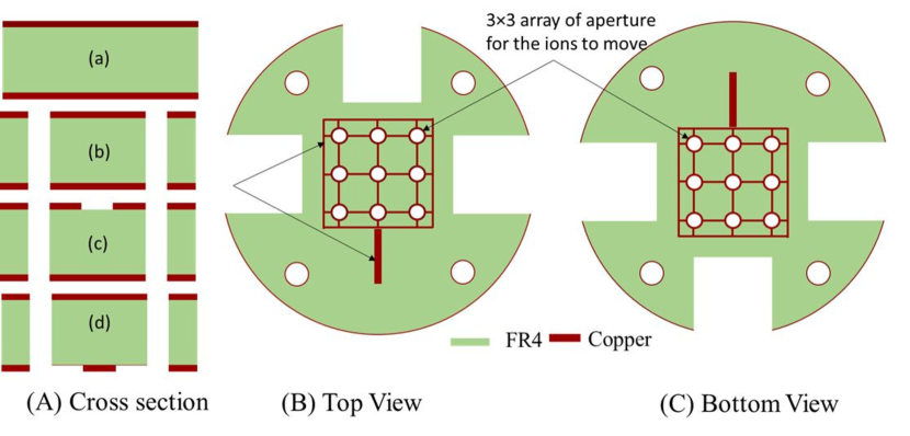
Using laser micromachining (LPKF ProtoLaser U4), top and bottom metal layers are patterned and holes are drilled through the PCB. Alignment between top and bottom is achieved by using an integrated vision system and pre-fabricated alignment fiducials. Steps of the process to fabricate RF wafers are given in Fig. 2. In this process, we start with a FR-4 based board that has copper on both sides as seen in the cross section [Fig. 2 (A)]. The circular holes are created using a laser tool. Then laser cutting is used to define top and bottom metal routing. The top and bottom views of the fabricated RF wafer are also shown in Fig. 2.
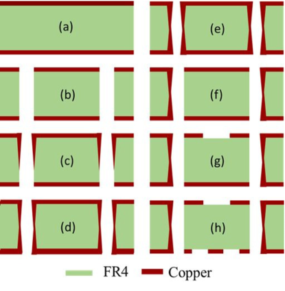
The main steps of the process to fabricate ESQ wafers are given in Fig. 3. The FR-4 based board has copper on both sides and holes are then created using the laser tool. As the holes in the PCBs are created using a scanned laser beam rather than a milling tool, arbitrary hole shapes can easily be realized. After cutting the holes, a copper layer ( thick) is evaporated onto the board in a conformal evaporator with a rotating chuck system on both sides. For better sidewall coverage, copper is also electroplated on top of the evaporated copper, which serves as a seed layer for the electroplated copper. The laser is then used to remove the metal on certain parts of the sidewalls of the holes to isolate the electrode. Finally, the laser is used again to define top and bottom metal routing.
IV Experimental Setup
To test the major components of this technology, a compact test stand has been set up. A filament driven, multi-cusp ion source Ji et al. (2016) is used to generate plasma. The source operates using argon or helium at a pressure in the plasma chamber of around 6 mTorr. To create the plasma, we rely on continuous gas flow rather than periodic gas puffs. The filament is then operated at several amperes and a -100 V arc pulse is applied for to ignite the plasma. Ions are extracted during the arc pulse by floating the source body to a high voltage (). Along with the plasma density, a three-electrode extraction system determines the plasma meniscus shape, extracted current density, and beamlet envelope trajectory at the high voltage acceleration gap (see Fig. 4). The plasma facing electrode (grid 1 in Fig. 4) is not electrically connected to a fixed voltage source and, therefore, floats to the plasma potential during operation. A voltage of has been measured during plasma operation. The second electrode (grid 2) is used to extract the ion beam and is biased at a negative voltage relative to the source body. A third electrode (grid 3) has been implemented that can be utilized to gate the extracted beam and short, uniform ion pulses of bunch duration with no electron pre-pulse have been achieved. However, in the work reported here, we do not utilize the gating mechanism and the third electrode is biased slightly more negative than the second grid, so that ions are extracted continuously during the arc-pulse. The ions then gain their remaining kinetic energy when they are accelerated from the source potential to a grounded exit aperture.
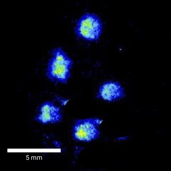
To demonstrate multiple parallel beamlets, we use a multi-aperture extraction system. In our prototype, a array of beam extraction apertures is implemented for each electrode, where each extraction aperture has a 0.5 mm diameter and the electrodes are positioned with an inter-hole pitch of 5 mm, see Fig. 5.
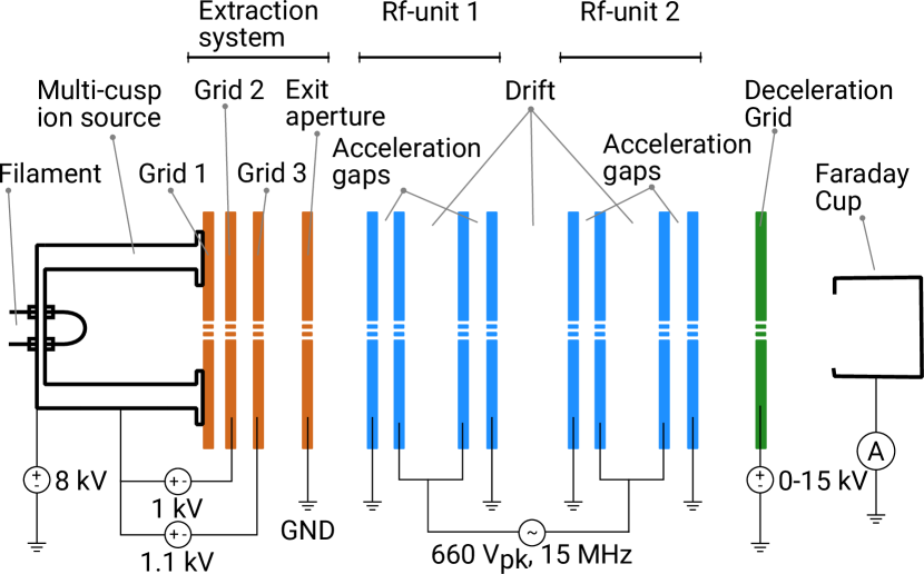
After the ions leave the beam extraction section, we utilize the beam to test our accelerator components. For the RF experiment, the test structure consisted of two RF units. The drift gap length was designed to match an 8 keV argon ion beam, a driving RF frequency of 15 MHz, and an acceleration voltage of 1 keV per gap. We summarize the implemented distances in our two RF-unit (four acceleration gaps) setup in Table 1.
| Drift gap number | Drift length (mm) |
|---|---|
| 1 | 4.00 |
| 2 | 4.37 |
| 3 | 4.73 |
The RF high-voltage for our experiments is generated by amplifying the output of a signal generator (Agilent 33520A) to an output power of at most 1 W (Mini Circuit ZHL-2-8) where it can be used to directly drive the gate of an RF metal–oxide–semiconductor field-effect transistor (MOSFET) and excite the tuned resonant circuit at the same frequency resulting in another gain of . This design is based on the RF generator for the buncher for the 88-inch cyclotron at Lawrence Berkeley National Laboratory (LBNL).Todd et al. (2013) The losses in the MOSFET and the RF wafer capacitance ( per gap) are the dominant loads. The frequency range used for the experiments presented here is 10-20 MHz. A peak amplitude on the PCB of up to 660 V has been measured.
In the absence of a pre-bunching (or chopper) section, the ion source will deliver a constant ion current over many RF periods. Therefore, some ions are expected to be accelerated and others decelerated. A retarding potential analyzer is used to measure the beam energy distribution. This is implemented by adding a biased grid after the RF units followed by a Faraday cup to measure the beam current. By scanning the grid voltage, the Faraday-cup at the end of the beamline selectively detects the current of ions with a kinetic energy higher than the bias voltage on the grid. For a larger accelerator structure, only a pulsed beam can be transported through the accelerator structure, since the focusing elements as well as the drift gaps will be tuned for a single ion energy. Without bunching the beam, one can expect a transport limit of about 10% of a continuous beam to be accelerated through an RF accelerator. This transport limit is given by the requirement for longitudinal phase stability.Wangler (2008)

The ESQ wafers are tested in a similar fashion. Instead of the RF units, a single ESQ wafer or a doublet is mounted downstream of the ion source. We then use a scintillator (RP 400 plastic scintillator) and a fast image intensifying camera (Princeton Instruments) to observe the beam transverse distribution. Since a filament driven ion source is being used, light from the filament is also detected by the camera. By looking at the scintillator at an angle, we avoid overlapping the light from the filament with light output from the ion beam hitting the scintillator. As both have roughly the same amplitude, this avoids the need for background subtraction. Voltage scans on the ESQ electrodes then result in beam deflection that can be measured.
V Results
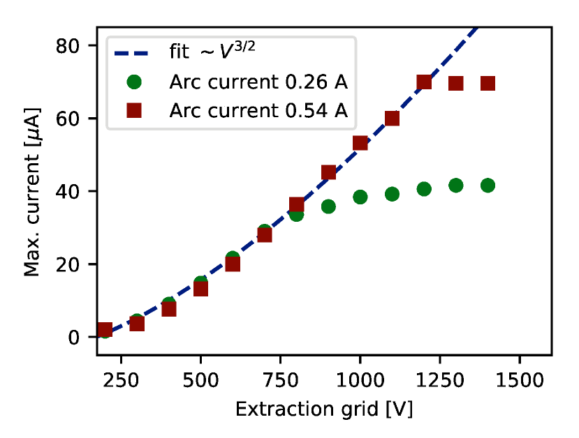
To characterize the ion source, we scanned the extraction voltages of the ion source. The source was operated at 6 mTorr using argon. The filament was on for 7 s to create a sufficiently high, stable filament temperature. Then the arc voltage was pulsed to -100 V for 0.3 ms. The source was floated at 8 kV and then extraction voltages on the second and third electrode were scanned. Here, the third electrode was always held 100 V more negative than the second electrode. Figure 6 shows the resulting beam current measured from the source without any RF or ESQ units present. The ion current increases as as expected from the Child-Langmuir law of space-charge limited extraction and then at higher extraction voltage, depending on the plasma density, changes to an emission limited regime. Operating the source in the emission limited regime will result in more shot-to-shot variation, since the output level will depend on the gas pressure in the source chamber, filament conditions, etc. Therefore, an operating point at an extraction voltage of 1000 V was chosen for an arc current of , which provided very stable source performance. The plasma facing electrode has diameter holes, thus the local extracted current density is at the operating point.
Next, two RF units were tested. The beam energy profile was measured for three different conditions: (1) minimum RF amplitude (lowest setting on the RF generator) (2) RF amplitude at 380 V amplitude and (3) RF amplitude at 660 V amplitude. The results are shown in Fig. 7 together with simulated results (solid lines). The simulation uses a 1-D model to calculate the beam energy of macro particles with nanosecond separation along the beam pulse. These particles are traced to the center of the acceleration gap where the particle energy is changed according to the RF phase at that time. Once the particles reach the position of the Faraday cup, a perfect energy filter is assumed and the charge of particles higher than the simulated retarding-grid voltage is integrated. The simulated results are based on the applied RF frequency and amplitude, the ion energy, mass and current, as well as the acceleration gap positions. The results of the simulation are then scaled to the initial beam current (the only free parameter in the simulation code). Experimental and simulation results using several RF gaps and the simulation program itself will be discussed in detail in a future publication.
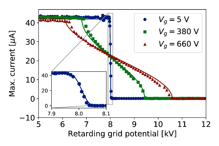
At the lowest RF settings of 5 V, an energy spread of about 15 eV is visible (see the inset of Fig. 7). This spread can be attributed to an intrinsic broadening of our diagnostic and fits well with a model from Sakai and KatsumataSakai and Katsumata (1985) that predicts a 15 eV energy resolution for a rectangular mesh of 90 lines/inch and as used in our experiment. The ion energy spread of a filament driven ion source is small,Lee et al. (1996) on the order of 5 eV. Since the energy spread within an RF-bucket will be more than an order of magnitude larger, the energy spread at the source is not explicitly included in the model. The measured injected beam energy is 8.01 keV based on the retarding potential scan. For the other cases, we measured a wider energy spread. As can be seen, some particles arrive at the correct time to achieve full acceleration in each gap, whereas others arrive at different phases of the RF and are either significantly accelerated, experience little or no acceleration or are significantly decelerated. This is to be expected, since we do not inject a pulsed beam but use a long pulse in regards to the RF frequency. In a linear accelerator, the stable longitudinal bucket occupies about 10% of the RF wave.Wangler (2008) In the absent of bunching, as in our present setup, we expect this fraction of the DC injected beam to be captured and accelerated through many gaps. This is in agreement with the data shown in Fig. 7. The measured energy distribution fits very well with our 1-D model that simulates a continuous ion beam. As one can see, the maximum beam energy is roughly given by the injected beam energy plus four times the maximum RF amplitude. The fact that the measured energy is slightly lower can be attributed to the fact that the gap distances were designed for a slightly higher RF amplitude. For a RF accelerator consisting of many stages, one would inject a pulsed beam or use a pre-buncher module to only inject particles at the right phase of the RF.
For the ESQ tests, we utilized a single ESQ wafer and demonstrated the characteristic elliptical deformation of a round beam that is the result of focusing the beam in one plane and at the same time defocusing the beam in the orthogonal plane (see Fig. 8).
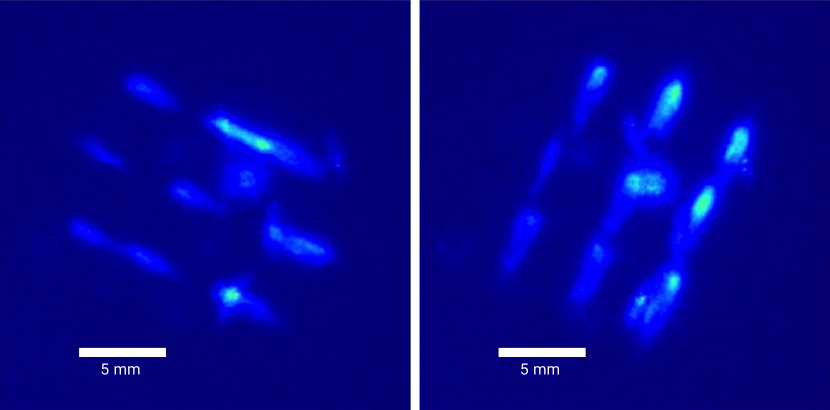
Combining two ESQs into a doublet then allows the beam to be focused in both directions. To demonstrate this, we chose voltages of an ESQ doublet such that the initial round beam is again focused to a round beam after passing two ESQs, as shown in Fig. 9. The radius of the focused round beam can be influenced by the applied voltages as expected.
VI Discussion
In this paper, we have demonstrated the functioning of basic components needed to implement a millimeter-scale MEQALAC formed from FR-4 PCB. The tested structures were made using a laser microfabrication tool that enables rapid prototyping for testing devices but is not the best in fabrication precision. The laser cutter provides resolution of over orifices of 100s of microns. Furthermore, the accuracy over a 4-inch PCB is made worse by the travel inaccuracies of the stages used to move the laser beam and the substrate. Another drawback of the laser microfabrication approach is that the speed of manufacturing is limited owing to the beam-based fabrication, much like exposure times in electron-beam lithography. However, our accelerator component design may be adapted to optical lithography fabrication in combination with silicon micromachining, which can lead to accuracy over a 4-inch wafer, while being fabricated in wafer-batches. These approaches are currently under development in our labs. By scaling our devices to be fabricated using silicon micromachining approach, we can achieve much greater uniform focusing elements leading to higher overall accelerator current densities.
The results reported here open a path to scaling to much higher ion beam currents and beam energies, which has the potential for ion beam systems in a broad series of established application areas where system cost and foot print can be reduced drastically. These results could also open up new application areas where system costs today make ion beam applications prohibitively expensive. Driver beams requirements to heat plasmas or targets for fusion energy are among the most demanding. Massively scaled MEMS multi-beam RF accelerators might offer a promising path for low cost ion beam fusion drivers. Our experiments have focused on accelerator technology and the demonstration of a scalable architecture to a large number of beams at a low cost. We have injected and transported in a array. The pitch of the array is 5 mm, thus, the average current density over a unit cell is: / . The quadrupole focusing results and the acceleration of the beam through two RF-units (two gaps per unit) show encouraging results, as shown in the preceding section.
The achieved beam current averaged over the array unit cell is still a long way from what is required for a fusion driver. To gauge the remaining challenges, consider a xenon driver beam (singly ionized) at 1 MeV for an unspecified fusion target requiring 1 MJ of beam energy in a pulse. We consider half of the surface area, steradians, of a 5 m radius fusion chamber will be occupied by about 2000 MEMS accelerators comprised of 30 cm diameter wafers within a vacuum enclosure. Each accelerator module must deliver 500 A of ions, and the peak current density averaged over a beamlet unit cell must be ca . To estimate the achievable beam parameters in a MEMS accelerator using demonstrated ion source technology, we assume that the ion sources deliver , as achieved previously for argon beams.Kwan, Grote, and Westenskow (2004) Assuming an aperture radius of 0.5 mm (as for the PCB ESQs tested above) and quadrupole electrode voltage of 2.5 kV, the peak field between the electrodes is 100 , a conservative design specification. Thus, the current density over a beamlet unit cell would be . This is lower by a factor of about than the needed current density for a driver. (For fusion target designs accommodating higher ion kinetic energy, the required current density decreases proportionally.) Strategies for reducing this could be a combination of source and injector improvements,Grote, Henestroza, and Kwan (2003) improved beam capture efficiency into the RF structure, and macro-bunch compression after the RF accelerator.Qin et al. (2005) These will be explored in future work and we note that they have been explored already for heavy ion driven inertial fusion system designs.
We envision this technology to be applicable for ion beams in the 100 keV to several MeV range, with average beam current densities up to . The technology can also be used for lower energies. However, below 100 keV it will be more effective to use a single high voltage gap to accelerate the ions directly. Above 100 keV beam energy, the advantages of having inexpensive components and lower peak voltages will be more and more important. For this technology to be competitive, we believe that an RF amplitude of several kilovolts is needed per acceleration gap. This way, we will be able to achieve gradients of 1 for the accelerator structure at frequencies in the 50 MHz range. To accomplish these high gradients, we are currently investigating the use of onboard resonators with a high Q that already have been shown to produce the required voltages. First prototypes are currently being designed and we will test these devices in the coming months to be able to integrate most of the RF stack onto the wafers. Switching from PCB to silicon will also provide a path for mass fabrication and better manufacturing precision.
In comparison to other current technologies, for example radio frequency quadrupoles (RFQs), MEQALACs can achieve higher total transported currents utilizing multiple beamlets. The overall energy efficiency of a MEQALAC also scales favorable in comparison to RFQs. A detailed comparison of these two technologies can be found in the paper of Urbanus et al.Urbanus et al. (1990) Another interesting metric is the effective transportable current density in respect to the cross section of the device (instead of the beam diameter). For state of the art RFQs of the order of (50 mA in a diameter vacuum chamber) has been established.Ratti et al. (2002) Our prototype MEQALAC design delivers around (, ). However, denser packaging can increase these by a factor of 10-30 in PCB implementations and the use of MEMS and silicon substrates will allow scaling to even higher current densities of the order of .
VII Conclusion and Outlook
We have shown that a compact RF unit without a resonant cavity can be used to accelerate an ion beam. For this proof of concept, PCB structures have been used, whereas for a final accelerator we envision the use of silicon micromachined wafers. This will allow smaller beamlets packed to a higher density on a wafer for increased effective beam-current densities. Furthermore, focusing elements in the form of ESQs will be added to the accelerator to allow for beam transport and refocusing of the beam along the beamline. Once we achieved integration of RF units and ESQ doublets, we will start scaling the concept to a stack of 10 RF units. This will allow us to examine scaling laws to higher energies. Initial simulations indicate that higher energies and currents will be achievable.
Acknowledgements.
We are grateful for insightful discussions with Andris Faltens (LBNL). This work was supported by the Office of Science of the US Department of Energy through the ARPA-E ALPHA program under contract DE-AC02–05CH11231 (LBNL).References
- Takatsu (2011) H. Takatsu, “ITER project and fusion technology,” Nucl. Fusion 51, 094002 (2011).
- Hemsworth et al. (2009) R. Hemsworth, H. Decamps, J. Graceffa, B. Schunke, M. Tanaka, M. Dremel, A. Tanga, H. P. L. De Esch, F. Geli, J. Milnes, T. Inoue, D. Marcuzzi, P. Sonato, and P. Zaccaria, “Status of the ITER heating neutral beam system,” Nuclear Fusion 49, 045006 (2009).
- Nuckolls et al. (1972) J. Nuckolls, L. Wood, A. Thiessen, and G. Zimmerman, “Laser compression of matter to super-high densities: Thermonuclear (CTR) applications,” Nature 239, 139–142 (1972).
- Bangerter, Faltens, and Seidl (2013) R. O. Bangerter, A. Faltens, and P. A. Seidl, “Accelerators for inertial fusion energy production,” Reviews of Accelerator Science and Technology 06, 85–116 (2013).
- Lindemuth and Siemon (2009) I. R. Lindemuth and R. E. Siemon, “The fundamental parameter space of controlled thermonuclear fusion,” American Journal of Physics 77, 407 (2009).
- Wurden et al. (2016) G. A. Wurden, S. C. Hsu, T. P. Intrator, T. C. Grabowski, J. H. Degnan, M. Domonkos, P. J. Turchi, E. M. Campbell, D. B. Sinars, M. C. Herrmann, R. Betti, B. S. Bauer, I. R. Lindemuth, R. E. Siemon, R. L. Miller, M. Laberge, and M. Delage, “Magneto-inertial fusion,” Journal of Fusion Energy 35, 69 (2016).
- Shi and Lal (2011) Y. Shi and A. Lal, “Integrated all-electric high energy ion beam guidance on chip: Towards miniature particle accelerator,” in 2011 IEEE 24th International Conference on Micro Electro Mechanical Systems (Institute of Electrical and Electronics Engineers (IEEE), 2011) pp. 137–140.
- Maschke (1979) A. Maschke, “Space-charge limits for linear accelerators,” Tech. Rep. BNL-51022 (Brookhaven National Lab., 1979).
- Hogan, Bangerter, and Kulcinski (1992) W. J. Hogan, R. Bangerter, and G. L. Kulcinski, “Energy from inertial fusion,” Physics Today 45, 42–50 (1992).
- Faltens and Seidl (1996) A. Faltens and P. Seidl, “Development of electrostatic quadrupoles for heavy ion fusion,” in Proceedings of 17th International Symposium on Discharges and Electrical Insulation in Vacuum, Vol. 1 (1996) pp. 478–481.
- Slade and Taylor (2002) P. G. Slade and E. D. Taylor, “Electrical breakdown in atmospheric air between closely spaced (0.2 m - 40 m) electrical contacts,” IEEE Transactions on Components and Packaging Technologies 25, 390–396 (2002).
- Skalyga et al. (2016) V. Skalyga, I. Izotov, S. Golubev, A. Sidorov, S. Razin, A. Vodopyanov, O. Tarvainen, H. Koivisto, and T. Kalvas, “New progress of high current gasdynamic ion source (invited),” Review of Scientific Instruments 87, 02A716 (2016).
- Ji et al. (2016) Q. Ji, P. A. Seidl, W. L. Waldron, J. H. Takakuwa, A. Friedman, D. P. Grote, A. Persaud, J. J. Barnard, and T. Schenkel, “Development and testing of a pulsed helium ion source for probing materials and warm dense matter studies,” Review of Scientific Instruments 87, 02B707 (2016).
- Todd et al. (2013) D. S. Todd, J. Y. Benitez, M. K. Covo, K. Y. Franzen, C. M. Lyneis, P. P. L. Phair, and M. M. Strohmeier, “High current beam extraction from the 88-inch cyclotron at lbnl,” in Proceedings of Cyclotrons2013 (2013) pp. 19–21.
- Wangler (2008) T. Wangler, RF Linear Accelerators, Physics textbook (Wiley, 2008) Chap. 6.
- Sakai and Katsumata (1985) Y. Sakai and I. Katsumata, “An energy resolution formula of a three plane grids retarding field energy analyzer,” Japanese Journal of Applied Physics 24, 337–341 (1985).
- Lee et al. (1996) Y. Lee, R. Gough, W. Kunkel, K. Leung, L. Perkins, D. Pickard, L. Sun, J. Vujic, M. Williams, and D. Wutte, “A compact filament-driven multicusp ion source,” Nuclear Instruments and Methods in Physics Research Section B: Beam Interactions with Materials and Atoms 119, 543–548 (1996).
- Kwan, Grote, and Westenskow (2004) J. W. Kwan, D. P. Grote, and G. A. Westenskow, “High current density beamlets from a rf argon source for heavy ion fusion applications,” Review of Scientific Instruments 75, 1838–1840 (2004).
- Grote, Henestroza, and Kwan (2003) D. P. Grote, E. Henestroza, and J. W. Kwan, “Design and simulation of a multibeamlet injector for a high current accelerator,” Phys. Rev. ST-AB 6, 014202 (2003).
- Qin et al. (2005) H. Qin, R. C. Davidson, J. J. Barnard, and E. P. Lee, “Drift compression and final focus options for heavy ion fusion,” Nucl. Instr. Meth. A 544, 255–261 (2005).
- Urbanus et al. (1990) W. H. Urbanus, R. G. C. Wojke, J. G. Bannenberg, H. Klein, A. Schempp, R. W. Thomae, T. Weis, and P. W. Van Amersfoort, “Comparison of two types of low- RF linacs: MEQALAC and RFQ,” Nucl. Instr. Meth. A 290, 1–10 (1990).
- Ratti et al. (2002) A. Ratti, J. Ayers, L. Doolittle, R. DiGennaro, R. A. Gough, M. Hoff, R. Keller, R. MacGill, J. Staples, R. Thomae, S. Virostek, R. Yourd, and A. Aleksandrov, “The sns front-end commissioning,” Proceedings of LINAC2002 , 329–331 (2002).