Trap assisted tunneling and its effect on subthreshold swing of tunnel field effect transistors
Abstract
We provide a detailed study of the interface Trap Assisted Tunneling (TAT) mechanism in tunnel field effect transistors to show how it contributes a major leakage current path before the Band To Band Tunneling (BTBT) is initiated. With a modified Shockley-Read-Hall formalism, we show that at room temperature, the phonon assisted TAT current always dominates and obscures the steep turn ON of the BTBT current for common densities of traps. Our results are applicable to top gate, double gate and gate all around structures where the traps are positioned between the source-channel tunneling region. Since the TAT has strong dependence on electric field, any effort to increase the BTBT current by enhancing local electric field also increases the leakage current. Unless the BTBT current can be increased separately, calculations show that the trap density has to be decreased by 40-100 times compared with the state of the art in order for the steep turn ON (for III-V materials) to be clearly observable at room temperature. We find that the combination of the intrinsic sharpness of the band edges (Urbach tail) and the surface trap density determines the subthreshold swing.
I Introduction
The Tunnel Field Effect Transistor (TFET) Seabaugh and Zhang (2010) is a candidate for low power switching in digital logic circuits for replacing or supplementing standard CMOS technologies because of its potential to reduce power dissipation via reduction of the power supply voltage. In a TFET, over-the-barrier thermionic emission is completely bypassed by triggering a BTBT current by the gate voltage, allowing steep “subthermal” change of current and reduced supply voltage. It has been shown that a small reduction in the subthreshold swing (SS) (e.g. to 45-53 mV/dec) in TFET can reduce the dynamic power dissipation by at least 50% Avci et al. (2013); Young et al. (2015) with little sacrifice on the switching delay. Such energy saving is calculated for the same OFF current but lower ON current (compared to the CMOS). The energy savings may enable high frequency operation that currently CMOS cannot provide. Further improvement is possible if higher ON current is achieved, which can be done with III-V semiconductors and heterojunctions Knoch and Appenzeller (2010).
However, the ideal picture of TFET operation is based upon the assumption that the Band To Band Tunneling (BTBT) current is sufficiently higher than any background current that flows before the bands overlap. In an ideal TFET operation, very little current should flow for gate voltages below a threshold voltage (defined as the gate voltage when the conduction band bottom in the channel and the valence band extrema in the source first overlap) and a large amount of current should flow above that. Such notion of steep (or ideal) switching is practically difficult to achieve since the combined leakage current, e.g. gate or substrate leakage, bulk or interface trap assisted tunneling will always be present and can easily obscure steep change of the BTBT current near the threshold voltage. In addition, the steepness of the current change partly depends on the BTBT magnitude and since it can be weak for multiple reasons, achieving the steep change of current is highly challenging. Despite numerous efforts in this field, experimental demonstrations with steep turn ON are few Appenzeller et al. (2004); Choi et al. (2007); Krishnamohan et al. (2008); Jeon et al. (2010); Dewey et al. (2011); Gandhi et al. (2011) and mostly at very low current levels. Most of the demonstrations involved silicon, for which the interface and bulk defect density is by far the best compared to other materials. Except for Refs. Dewey et al. (2011); Ganjipour et al. (2012), most TFET experimental results on III-V semiconductors Mookerjea et al. (2010); Yu et al. (2015); Zhao et al. (2014) do not show subthermal switching. On the contrary the subthreshold swing in these experiments shows strong temperature dependence, clearly indicating the existence of a thermal process. Two dimensional layered heterostructure based TFETs have attracted significant attention in recent times with one experiment Sarkar et al. (2015) showing low subthreshold swing. But similar structures by other groups Roy et al. (2015); Nourbakhsh et al. (2016) have failed to produce such behavior.
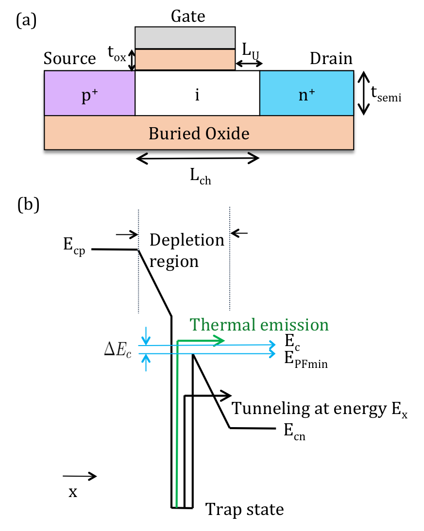
In this work, we show that interface trap assisted tunneling (TAT) current, which is known as a leakage current mechanism in conventional junction diodes Schenk (1992); Hurkx et al. (1992), is also a major parasitic current component in TFETs. TAT is the emission of electrons to a trap state via electron-phonon interaction, followed by tunneling into the conduction band (Fig. 1). Similarly a hole emission and tunneling from a trap is possible. This process is strongly temperature dependent compared to other non-idealities such as exponential band tails from the heavy source doping Khayer and Lake (2011). Such interband transition is also possible when phonon scattering is considered alone. Models with phonon scattering (without traps) have shown higher OFF current without sacrificing much on the subthreshold swing Koswatta et al. (2008). Although TAT has been identified in the past as a leakage mechanism in TFETs Mookerjea et al. (2010); Vallett et al. (2010); Pala and Esseni (2013); Qiu et al. (2014); Avci et al. (2015); Agarwal and Yablonovitch (2015), a detailed quantitative study of its deleterious effects has not been performed. We show that in the presence of traps, electron capture rate prescribed by the Shockley-Read-Hall (SRH) formalism is greatly enhanced due to the high electric field near the source. This is due to the fact that the undesirable electron tunneling from trap to conduction band depends on the local electric field (Fig. 2), in much the same way as the ON state BTBT current. We show that at room temperature this TAT current overshadows the steepest part of the BTBT current (Fig. 3) for realistic trap density (midgap /cm2-eV for III-V). The steep turn ON of the BTBT current is observable at low temperatures, where the BTBT dominates and the subthreshold swing becomes less temperature dependent. In our model, we consider the Poole-Frenkel effect Furlan (2001) - the lowering of the electron barrier due to the Coulomb interaction of the trap with the lattice. We find that the Poole-Frenkel effect causes a substantial increase in the leakage current by enhancing the trap-channel tunneling. In the next section, we review the electric field dependent SRH formalism, the electrostatic model and the BTBT model used in this paper followed by discussions. The formalism is also applicable to most other device geometries and materials provided that the is known and the electrostatic configuration is solved appropriately.
II Model description
In this section, we review the electric field enhanced carrier generation rate via phonon and trap states. We incorporate the Poole-Frenkel effect and the tunneling enhanced rates as done in Refs. Hurkx et al. (1992); Furlan (2001) but apply them using the TFET electrostatics and consider only the surface trap states. The electric field profile from the electrostatic model is used in calculating both the TAT and BTBT current.
II.1 Trap assisted tunneling
The classical SRH formalism Sze and Ng (2006) describes the generation rate of electron and hole pairs in presence of traps. An electron in the valence band (VB) can absorb a phonon to reach a trap state before emitting to the conduction band (CB) by interaction with another phonon. However, in the presence of electric field, the trap-CB (or VB-trap) tunneling rate becomes substantial and greatly increases the electron-hole generation rate Hurkx et al. (1992). The net generation rate (per unit area) at a given position in the junction space charge region becomes,
| (1) |
where is the intrinsic carrier concentration, and are the electron and hole densities, is the minority carrier lifetime and is a factor that accounts for the tunneling from trap to CB. With , Eq. 1 reduces to the classical SRH formalism. The carrier lifetime depends upon the capture cross section and the thermal velocity, . is electric-field-dependent and it effectively decreases the minority carrier lifetime. When the electric field is weak, is negligible and Eq. 1 reduces to the classical SRH formalism. The terms and arise from the principle of detailed balance Sze and Ng (2006) and are given by , , where and are the position of the Fermi level for intrinsic semiconductor and the trap state. Fig. 1b schematically shows the TAT, which is a two-step process. In the first step, the electron is emitted from the valence band to the trap state by absorbing a phonon. Afterwards, the electron can be partially lifted further and then tunnel into the conduction band. The amount of the partial lift in the second step can vary from , the position of the CB in the channel, to the position of the CB at the position under consideration. Within the energy range , electrons reach the conduction band without any resistance since there is no barrier to tunnel, whereas for , the transmission probability through the barrier has to be accounted for. Therefore the enhancement factor is the sum of two components, one for each energy regime
| (2) |
is calculated from the net flux (carrier density times the thermal velocity) and the transmission probability Furlan (2001),
| (3) |
is the energy to which the electron (or hole) is tunneling to (Fig. 1b). is calculated for a triangular barrier using the Wentzel-Kramers-Brillouin (WKB) approximation.
| (4) |
where is the electric field at a particular position in the depletion regime for a given gate voltage. For , . From Eq. 3 it can be shown,
| (5) | |||||
where is the lowering of the barrier (Fig. 1b) due to the Poole-Frenkel effect. is effectively the tunnel barrier height and it also defines the range of energy to which the electron (or hole) can tunnel to (from the trap). So is the difference between the top of the barrier and the minimum energy where the electron can tunnel to. Depending upon the position (in the depletion region) under consideration, this can vary from (if ) to (if ) Hurkx et al. (1992). The higher the Poole-Frenkel effect, the higher the and the higher the ’s in Eq. 5. For typical electric fields, the second term in Eq. 5 (which signifies the tunneling contribution), dominates over the first term and increases the exponential term for smaller or larger . The lowering of the energy barrier is determined by the electric field Woo et al. (1987); Pelaz et al. (1994); Huang et al. (1997) , where is the electric permittivity. The ’s are calculated for both electron and hole (so that all combinations of phonon absorption and tunneling as shown in Fig. 1b are included in the model) and used in Eq. 1.
Performance degradation in TFET can take place even without the traps due to inelastic phonon scattering Koswatta et al. (2008); Yoon and Salahuddin (2012). The OFF current is increased in addition to making the transfer I-V ambipolar. But the phonon limited subthreshold swing can still be less than 60 mV/dec. Traps on the other hand increase the carrier capture rates to a large extent so that the leakage current dominates over the desired current. TAT affects both the ON-OFF current ratio and the subthreshold swing.
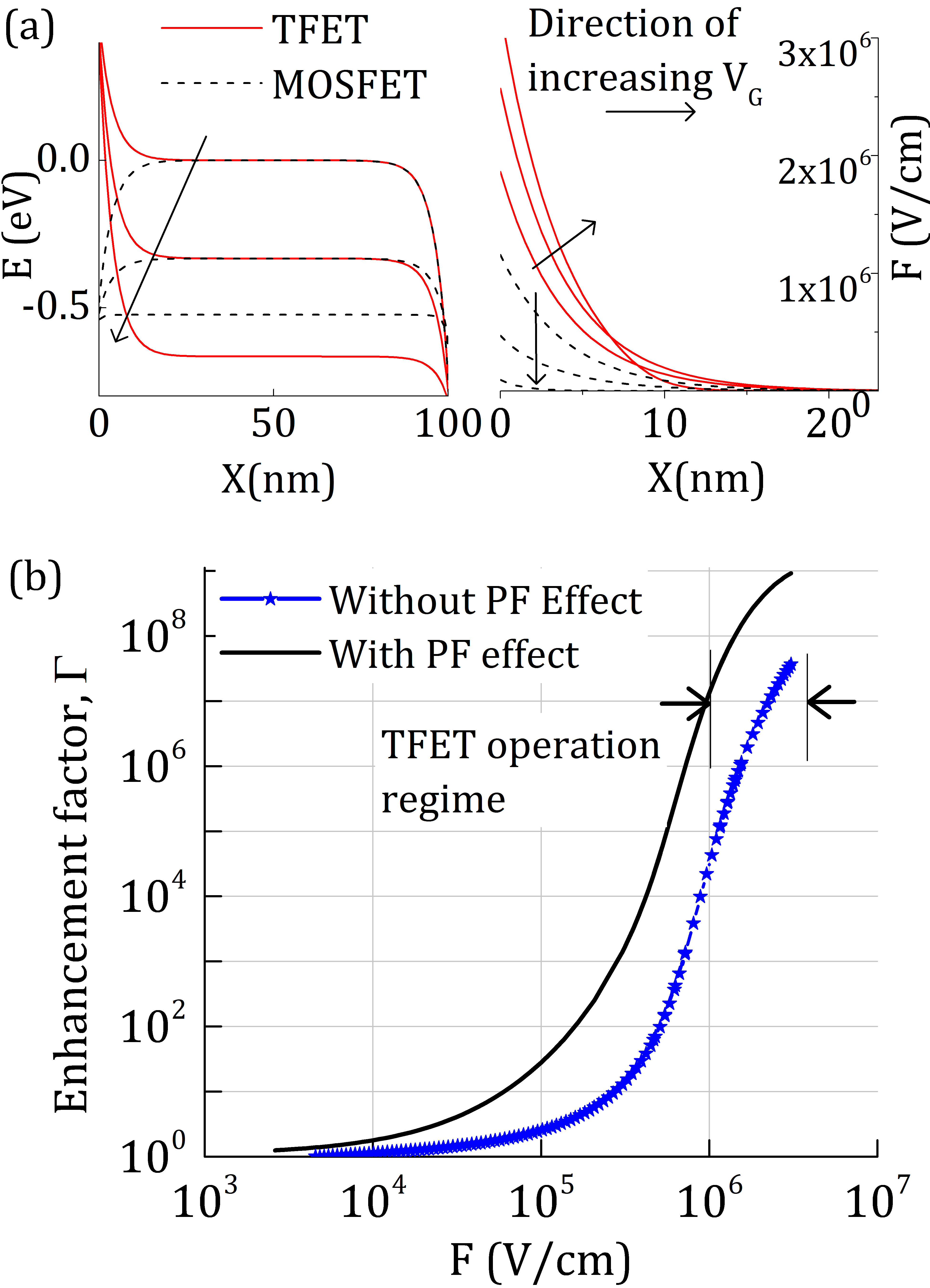
Fig. 2b shows the total enhancement (Eq. 2) in silicon with and without the Poole-Frenkel effect. can be as high as , which is effectively the enhancement of the SRH rate. Typical TFET electric fields operate around V/cm, over which the changes by less than two orders of magnitude.
Finally the current is calculated from,
| (6) |
II.2 Electrostatic model
As derived in Yan et al. (1992), we use an abridged version of the 2D Poisson equation for the top gate structure shown in Fig. 1a. For an SOI structure, the electric field at the top and bottom surface of the semiconductor (given by the oxide thickness and gate potentials) can be applied to the 2D Poisson equation and can be simplified as
| (7) |
where is the surface potential and is the gate potential. Eq. 7 captures the 2D electrostatics quite well for a given characteristic length . For the top gated architecture, . The charge density in the channel is mainly dictated by the drain injection, since the channel is poorly coupled to the source
| (8) |
where and are the equilibrium electron concentration in the channel. Eqs. 7 and 8 are solved iteratively until self-consistency is achieved. For a given , the potential is calculated numerically from Eq. 7 using the finite difference method subject to appropriate boundary conditions (for the doped regions). Eq. 7 is also valid for double-gate and gate-all-around nanowire structure if the characteristic length is changed appropriately Yan et al. (1992).
Fig. 2a (left) shows the conduction band profile. On the right, we show the electric field for various gate voltages. For the TFET configuration, the electric field near the source end is greatly enhanced. For a MOSFET configuration on the other hand, the energy barrier (and the conduction band) is pushed down resulting in a decreased electric field near the source. This opposite trend in the electric field with gate voltage, results in a drastically different TAT current in TFET compared to MOSFET since the TAT is dependent on the local electric field. The TAT for TFETs increases with gate voltage, while for MOSFETs it diminishes quickly (not shown). Therefore the role of traps in MOSFETs is mostly limited to a decreased gate efficiency, while for TFETs, it affects both the gate efficiency and leakage. In this paper, we did not account for the impact of reduced gate efficiency due to . Including it would only increase the subthreshold swing relative to what we show (depending on trap density and gate dielectric thickness).
II.3 BTBT model
The transmission probability through the tunnel barrier is determined by the WKB approximation Seabaugh and Zhang (2010). It can be written as,
| (9) |
where , , and are material parameters taken from Kao et al. (2012) and Lu et al. (2015). is the tunnel window, i.e. the energy difference between the valence band in the source and the conduction band in the channel; it is determined by an Urbach tail below the threshold voltage and it increases linearly with gate voltage above the threshold voltage Lu et al. (2015). . A difference between Ref. Lu et al. (2015) and our approach is that we find the position of the conduction band after self-consistency is achieved between carrier density and channel potential, as discussed in previous sub-section. So for any given gate voltage, the position of the conduction band is . is the Urbach parameter and it determines the intrinsic subthreshold swing.
The Urbach tail has been studied in the past in order to understand the sharpness of the optical absorption spectrum in semiconductors. Instead of a steep rise in the absorption co-efficient above a threshold photon energy, experimental results typically show an exponential rise following Pankove (1965); Urbach (1953). Such non-abrupt absorption has been attributed to the Urbach tail which originates in heavily doped semiconductors from the smearing of the dopant energy levels. It can also happen in undoped semiconductors due to electron-phonon interaction Subashiev et al. (2010) with a lower Urbach parameter . The temperature variation of is weak in doped semiconductors compared to an undoped one Johnson and Tiedje (1995). Unfortunately the exact nature of the Urbach tail and its temperature dependence of is not well understood Greeff and Glyde (1995). In the next section, we will discuss the implication of various cases of Urbach tail and how it affects the TFET performance.
III Results and discussion
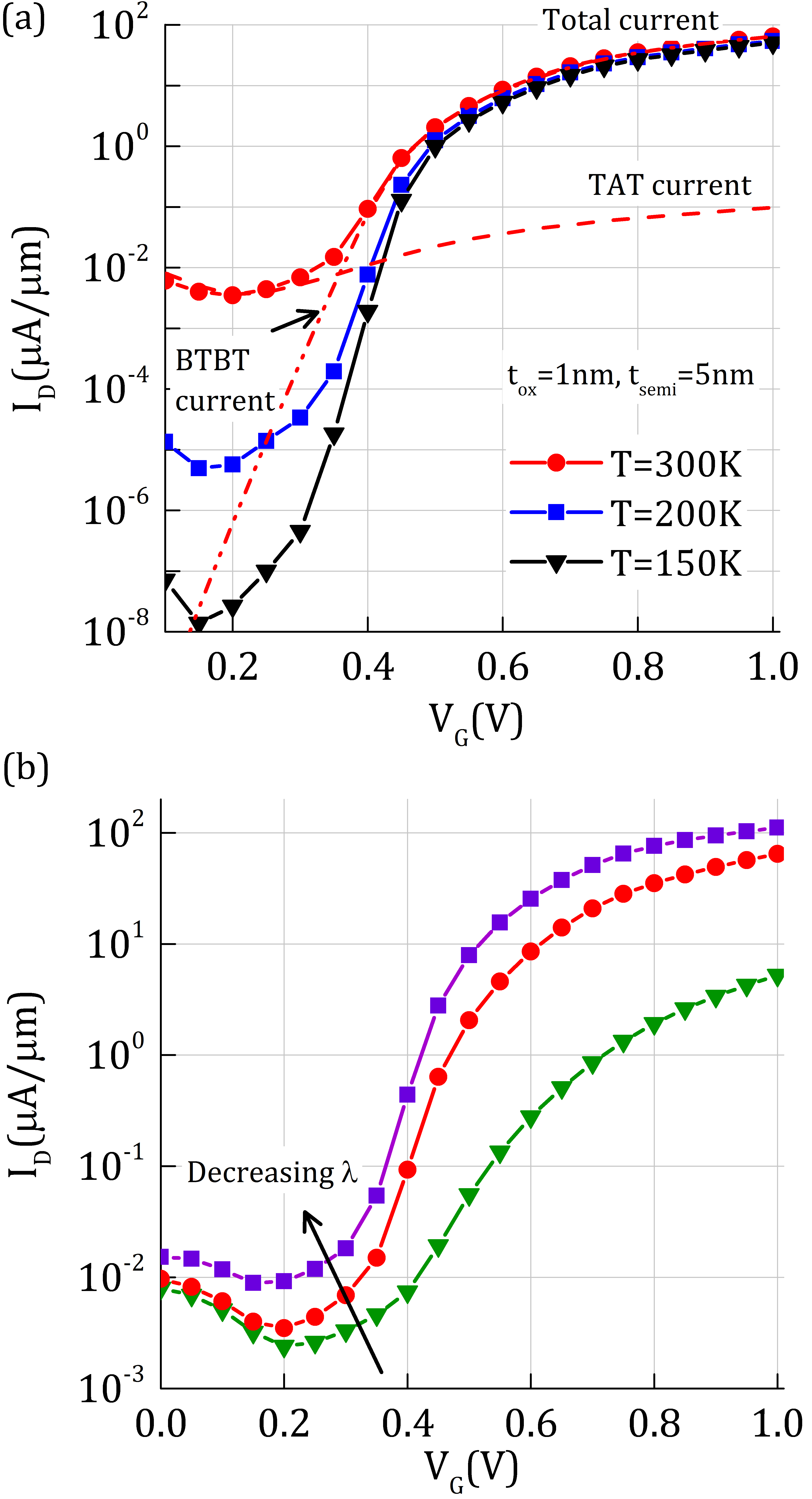
We apply the model for the top gate structure shown in Fig. 1a. Effective oxide thickness (EOT), and semiconductor body thickness are 1 nm and 5 nm respectively. profile in Ref. Brammertz et al. (2009) is used for III-V with midgap of cm2-eV. Although is a function of energy in the bandgap, we found that in most cases the midgap trap density dominates the trap current. Channel length, is 100 nm. Source and drain contact regions are degenerately doped while the channel is undoped. The capture cross-section for electrons, holes are , Furlan (2001); Selberherr (2012) and the carrier lifetimes are calculated from there using the thermal velocity, . An underlap (10 nm long) at the channel-drain end is used to suppress the electric field in the drain end and therefore the ambipolarity. For the transfer curves, we use a drain bias V. We ignore channel resistance due to carrier scattering in the channel since the resistance due to TAT and BTBT is substantially higher.
Fig. 3a shows the transfer plots for In0.53Ga0.47As TFET at various temperatures. For room temperature, the TAT and BTBT current components of the total current are also shown. Well above the threshold voltage ( V), the total current mainly comes from BTBT. The TAT current is just enough so that it intersects with the BTBT current near the threshold voltage, therefore the total current below is dominated by the TAT. The TAT thus obscures the steepest part of the BTBT ( 40 mV/dec in this calculation) and so the minimum subthreshold swing ( 75 mV/dec) is limited by the rate of change of BTBT current just above the threshold voltage. This subthreshold swing will get much worse for thicker oxide and body thickness. Such transfer behavior with a valley near the minimum current is seen in most experiments on III-V TFETs Yu et al. (2015); Mohata et al. (2012); Pandey et al. (2015). At lower temperatures, electron hole generation rate is reduced leading to lower TAT. For temperatures lower than 200 K, intrinsic subthreshold swing is observed. The current above the threshold voltage is weakly dependent on temperature while current below the threshold varies stongly with temperature. In other words, the lowest achievable current at any given temperature is a function of temperature (decreases from 1 nA at 300 K to 10 fA at 150 K), similar to what is seen in the experiments Mookerjea et al. (2010); Yu et al. (2015); Zhao et al. (2014); Mookerjea et al. (2009); Noguchi et al. (2013).
To demonstrate the effect of the scaling length and the local electric field, Fig. 3b shows the transfer plots for different oxide and body thicknesses at T = 300 K. With nm and nm (violet squares), ON current increases substantially due to the increase of the local electric field near the source. Subthreshold swing also improves to 65 mV/dec which is still not subthermal. This is due to the fact that the TAT current has also increased, thus limiting the advantage of the higher electric field. We infer that the same effect takes place in heterojunction TFETs, making it difficult to observe subthermal switching for those structures as well.
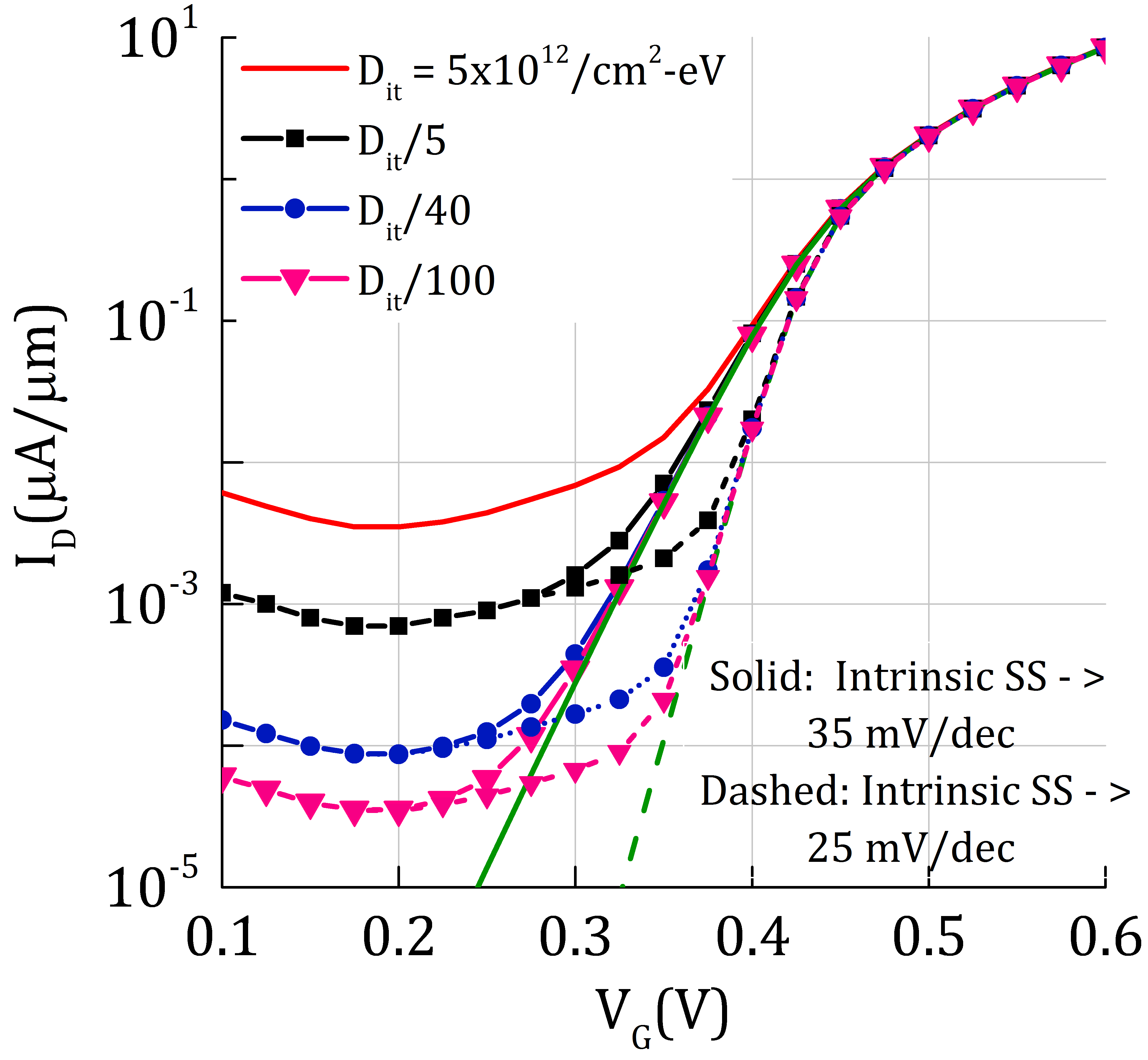
Fig. 4 shows the transfer plots for various trap density for two different intrinsic subthreshold swings (Urbach tails at 35 and 25 mV/dec) with a motivation to find the trap density required to achieve subthermal switching for multiple decades. We find that a trap density of 1.2510-eV, which is about 40 times smaller than today’s typical midgap trap density, achieves about two orders of current change at 40 mV/dec. For the steeper intrinsic swing, we again get two orders of current change at subthermal rate ( 28 mV/dec). In this case, the TAT and BTBT intersects at a higher . Since the TAT increases with , a steeper Urbach tail does not necessarily increase the ON-OFF ratio (at subthermal rate). Therefore the ON-OFF ratio at subthermal rate is determined mainly by the trap density, while the subthreshold swing is determined by the Urbach tails. We see this again when the trap density is reduced by 100 times, where we get about three orders of change in current at subthermal rate for both Urbach tails.
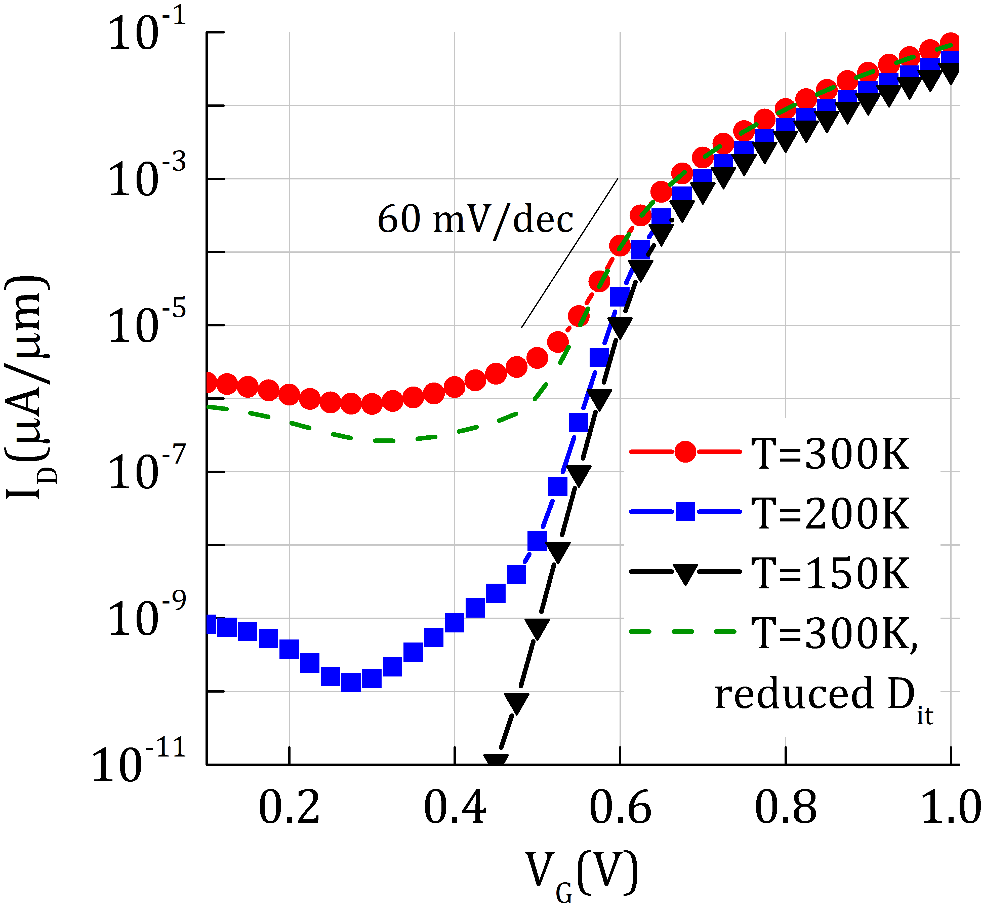
We applied the same model to silicon to see how the transfer characteristic changes at reduced trap density and different material properties. In Fig. 5, we see that both BTBT and TAT decrease substantially due to heavier effective mass and higher bandgap with a midgap trap density of /cm2-eV, which is typical in today’s silicon technology. Similar to III-V, the steepest part of the BTBT is not seen due to the TAT. However at /cm2-eV, we found (dashed line) two orders of current change at 50 mV/dec (in pA range). Such is much easier to achieve in silicon than the requirements mentioned earlier for III-V. This also explains, why most experiments reporting margin subthermal switching at very low currents involved silicon, where it is likely that such trap density may be achieved.
IV Conclusion
We provide an analysis of the parasitic trap assisted tunneling current in TFETs. We show that in most cases, the subthreshold current in TFETs is dominated by TAT, regardless of channel material. The takeover from TAT to band to band tunneling depends on the temperature, electrostatic characteristic length, material parameters (e.g. effective mass) and the rate of change of the exponential band tails (Urbach tails). We show that engineering efforts to increase the ON current are also likely to increase the subthreshold current, since both BTBT and TAT are driven by the same mechanism (tunneling through a barrier). The TAT current is much more deleterious than just the electron-phonon scattering without traps. We find that to get a reasonable ON-OFF ratio with steeper than 60 mV/dec subthreshold swing at room temperature, trap density has to be reduced by 40-100 times compared to the state of the art for III-V semiconductors, for reasonable structural device parameters.
V Acknowledgment
This work was supported by National Science Foundation under the Center for Energy Efficient Electronics Science Center, Award 0939514, and the NCN-NEEDS Program, Grant 1227020-EEC, with additional support by the Semiconductor Research Corporation. Authors also thank Eli Yablonovitch (UC Berkeley), Patrick Xiao (UC Berkeley), Sapan Agarwal (Sandia), Ujwal Radhakrishna (MIT), Alan Seabaugh (University of Notre Dame) for useful discussions.
References
- Seabaugh and Zhang (2010) A. C. Seabaugh and Q. Zhang, Proceedings of the IEEE 98, 2095 (2010).
- Avci et al. (2013) U. E. Avci, D. H. Morris, S. Hasan, R. Kotlyar, R. Kim, R. Rios, D. E. Nikonov, I. Young, et al., in Electron Devices Meeting (IEDM), 2013 IEEE International (IEEE, 2013), pp. 33–4.
- Young et al. (2015) I. Young, U. Avci, and D. Morris, in Electron Devices Meeting (IEDM), 2015 IEEE International (IEEE, 2015), pp. 25–5.
- Knoch and Appenzeller (2010) J. Knoch and J. Appenzeller, Electron Device Letters, IEEE 31, 305 (2010).
- Appenzeller et al. (2004) J. Appenzeller, Y.-M. Lin, J. Knoch, and P. Avouris, Phys. Rev. Lett. 93, 196805 (2004).
- Choi et al. (2007) W. Y. Choi, B.-G. Park, J. D. Lee, and T.-J. K. Liu, Electron Device Letters, IEEE 28, 743 (2007).
- Krishnamohan et al. (2008) T. Krishnamohan, D. Kim, S. Raghunathan, and K. Saraswat, in Electron Devices Meeting, 2008. IEDM 2008. IEEE International (IEEE, 2008), pp. 1–3.
- Jeon et al. (2010) K. Jeon, W.-Y. Loh, P. Patel, C. Y. Kang, J. Oh, A. Bowonder, C. Park, C. Park, C. Smith, P. Majhi, et al., in VLSI technology (VLSIT), 2010 symposium on (IEEE, 2010), pp. 121–122.
- Dewey et al. (2011) G. Dewey, B. Chu-Kung, J. Boardman, J. Fastenau, J. Kavalieros, R. Kotlyar, W. Liu, D. Lubyshev, M. Metz, N. Mukherjee, et al., in Electron Devices Meeting (IEDM), 2011 IEEE International (IEEE, 2011), pp. 33–6.
- Gandhi et al. (2011) R. Gandhi, Z. Chen, N. Singh, K. Banerjee, and S. Lee, Electron Device Letters, IEEE 32, 437 (2011).
- Ganjipour et al. (2012) B. Ganjipour, J. Wallentin, M. T. Borgström, L. Samuelson, and C. Thelander, ACS nano 6, 3109 (2012).
- Mookerjea et al. (2010) S. Mookerjea, D. Mohata, T. Mayer, V. Narayanan, and S. Datta, IEEE Electron Device Letters 31, 564 (2010).
- Yu et al. (2015) T. Yu, U. Radhakrishna, J. L. Hoyt, and D. A. Antoniadis, in Electron Devices Meeting (IEDM), 2014 IEEE International (IEEE, 2015).
- Zhao et al. (2014) X. Zhao, A. Vardi, J. del Alamo, et al., in Electron Devices Meeting (IEDM), 2014 IEEE International (IEEE, 2014), pp. 25–5.
- Sarkar et al. (2015) D. Sarkar, X. Xie, W. Liu, W. Cao, J. Kang, Y. Gong, S. Kraemer, P. M. Ajayan, and K. Banerjee, Nature 526, 91 (2015).
- Roy et al. (2015) T. Roy, M. Tosun, X. Cao, H. Fang, D.-H. Lien, P. Zhao, Y.-Z. Chen, Y.-L. Chueh, J. Guo, and A. Javey, ACS nano 9, 2071 (2015).
- Nourbakhsh et al. (2016) A. Nourbakhsh, A. Zubair, M. S. Dresselhaus, and T. Palacios, Nano letters (2016).
- Schenk (1992) A. Schenk, Solid-State Electronics 35, 1585 (1992).
- Hurkx et al. (1992) G. Hurkx, D. Klaassen, and M. Knuvers, Electron Devices, IEEE Transactions on 39, 331 (1992).
- Khayer and Lake (2011) M. A. Khayer and R. K. Lake, Journal of Applied Physics 110, 074508 (2011).
- Koswatta et al. (2008) S. O. Koswatta, M. S. Lundstrom, and D. E. Nikonov, Applied Physics Letters 92, 043125 (2008).
- Vallett et al. (2010) A. L. Vallett, S. Minassian, P. Kaszuba, S. Datta, J. M. Redwing, and T. S. Mayer, Nano letters 10, 4813 (2010).
- Pala and Esseni (2013) M. G. Pala and D. Esseni, Electron Devices, IEEE Transactions on 60, 2795 (2013).
- Qiu et al. (2014) Y. Qiu, R. Wang, Q. Huang, and R. Huang, Electron Devices, IEEE Transactions on 61, 1284 (2014).
- Avci et al. (2015) U. Avci, B. Chu-kung, A. Agrawal, G. Dewey, V. Le, R. Rios, D. Morris, S. Hasan, R. Kotlyar, J. Kavalieros, et al., in Electron Devices Meeting (IEDM), 2015 IEEE International (IEEE, 2015), pp. 25–5.
- Agarwal and Yablonovitch (2015) S. Agarwal and E. Yablonovitch, in Device Research Conference (DRC), 2015 73rd Annual (IEEE, 2015), pp. 247–248.
- Furlan (2001) J. Furlan, Progress in quantum electronics 25, 55 (2001).
- Sze and Ng (2006) S. M. Sze and K. K. Ng, Physics of semiconductor devices (John Wiley & Sons, 2006).
- Woo et al. (1987) J. Woo, J. D. Plummer, and J. Stork, Electron Devices, IEEE Transactions on 34, 130 (1987).
- Pelaz et al. (1994) L. Pelaz, J. L. Orantes, J. Vincente, L. A. Bailon, and J. Barbolla, IEEE Transactions on Electron Devices 41, 587 (1994).
- Huang et al. (1997) Q.-A. Huang, M. Qin, B. Zhang, J. K. Sin, and M. Poon, IEEE electron device letters 18, 616 (1997).
- Yoon and Salahuddin (2012) Y. Yoon and S. Salahuddin, Applied Physics Letters 101, 263501 (2012).
- Yan et al. (1992) R.-H. Yan, A. Ourmazd, and K. F. Lee, Electron Devices, IEEE Transactions on 39, 1704 (1992).
- Kao et al. (2012) K.-H. Kao, A. S. Verhulst, W. G. Vandenberghe, B. Soree, G. Groeseneken, and K. De Meyer, Electron Devices, IEEE Transactions on 59, 292 (2012).
- Lu et al. (2015) H. Lu, D. Esseni, and A. Seabaugh, Solid-State Electronics 108, 110 (2015).
- Pankove (1965) J. Pankove, Physical Review 140, A2059 (1965).
- Urbach (1953) F. Urbach, Physical Review 92, 1324 (1953).
- Subashiev et al. (2010) A. V. Subashiev, O. Semyonov, Z. Chen, and S. Luryi, Applied Physics Letters 97, 181914 (2010).
- Johnson and Tiedje (1995) S. Johnson and T. Tiedje, Journal of applied physics 78, 5609 (1995).
- Greeff and Glyde (1995) C. Greeff and H. Glyde, Physical Review B 51, 1778 (1995).
- Brammertz et al. (2009) G. Brammertz, H.-C. Lin, M. Caymax, M. Meuris, M. Heyns, and M. Passlack, Applied Physics Letters 95, 2109 (2009).
- Selberherr (2012) S. Selberherr, Analysis and simulation of semiconductor devices (Springer Science & Business Media, 2012).
- Mohata et al. (2012) D. Mohata, B. Rajamohanan, T. Mayer, M. Hudait, J. Fastenau, D. Lubyshev, A. W. Liu, and S. Datta, Electron Device Letters, IEEE 33, 1568 (2012).
- Pandey et al. (2015) R. Pandey, H. Madan, H. Liu, V. Chobpattana, M. Barth, B. Rajamohanan, M. Hollander, T. Clark, K. Wang, J.-H. Kim, et al., in VLSI Technology (VLSI Technology), 2015 Symposium on (IEEE, 2015), pp. T206–T207.
- Mookerjea et al. (2009) S. Mookerjea, D. Mohata, R. Krishnan, J. Singh, A. Vallett, A. Ali, T. Mayer, V. Narayanan, D. Schlom, A. Liu, et al., in Electron Devices Meeting (IEDM), 2009 IEEE International (IEEE, 2009), pp. 1–3.
- Noguchi et al. (2013) M. Noguchi, S. Kim, M. Yokoyama, S. Ji, O. Ichikawa, T. Osada, M. Hata, M. Takenaka, and S. Takagi, in Electron Devices Meeting (IEDM), 2013 IEEE International (IEEE, 2013), pp. 28–1.