Density Functional Theory based Study of Chlorine Doped WS2-metal Interface
Abstract
Investigation of a TMD-metal interface is essential for the effective functioning of monolayer TMD based field effect transistors (FETs). In this work, we employ Density Functional Theory (DFT) calculations to analyze the modulation of the electronic structure of monolayer WS2 with chlorine doping and the relative changes in the contact properties when interfaced with gold and palladium. We initially examine the atomic and electronic structures of pure and doped monolayer WS2 supercell and explore the formation of mid gap states with band splitting near the conduction band edge. Further we analyze the contact nature of the pure supercell with Au and Pd. We find that while Au is physiosorped and forms n-type contact, Pd is chemisorped and forms p-type contact with a higher valence electron density. Next, we study the interface formed between the Cl-doped supercell and metals and observe a reduction in the Schottky barrier height (SBH) in comparison to the pure supercell. This reduction found is higher for Pd in comparison to Au which is further validated by examining the charge transfer occurring at the interface. Our study confirms that Cl doping is an efficient mechanism to reduce the n-SBH for both Au and Pd which form different types of contact with WS2.
After the fabrication of FET using monolayer MoS2,Radisavljevic et al. (2011) 2D layered transition metal dichalcogenides(TMDs) have garnered enormous attention in the electron devices community. Apart from MoS2, other TMDs as such WS2Sik Hwang et al. (2012); Liu et al. (2014), WSe2Das and Appenzeller (2013), MoSe2Larentis, Fallahazad, and Tutuc (2012) and MoTe2Pradhan et al. (2014) are also explored as channel material for FET’s. In the absence of efficient doping techniques, these transistors exhibit SBH at source/drain contact which leads to low ON current. Tremendous efforts are dedicated to reduce the contact resistance at TMD-metal interface by employing different techniques both theoretically and experimentally.Leong et al. (2014); Chanana and Mahapatra (2015); Das et al. (2013); Kang, Liu, and Banerjee (2014); Laskar et al. (2014); Suh et al. (2014) However, most of these efforts are focused towards MoS2 and WSe2 and a minimum study is devoted to other TMD’s-metal contact interfaces. A study using ballistic MOSFET model reveals that WS2 outperforms all other TMD’sLiu et al. (2011). Experimental reports of WS2 device fabrication (Sik Hwang et al., 2012) and Cl doping technique for reducing WS2-metal contact resistance are also reportedYang et al. (2014). However, theoretical investigations of WS2 metal contact interface using first principles is still lacking in the literature. Since first principles are extensively used to analyze the graphene-metalKhomyakov et al. (2009); Gong et al. (2010), MoS2-metal Popov, Seifert, and Tománek (2012) and WSe2-metalKang et al. (2014), it is believed that it will efficiently describe the contact nature with other TMD’s as well. For WS2, chlorine doping, which is done by replacing sulfur atoms is the first ever method demonstrated experimentally to reduce the WS2-contact resistance, exhibiting both high drain current and field-effect mobility.Yang et al. (2014) In this work we employ density function theory (DFT) to study the electronic structure of the interface between WS2 and one physiosorped (Au) and one chemisorped (Pd) metal. We then examine the effect of chlorine doping by substituting sulfur atoms to address the SBH mitigation at WS2-metal interface.
We start by analyzing the electronic dispersion characteristics of pure and Cl-doped WS2 and explore the shifts in the energy bands with respect to Fermi level (Ef) and further analyze the mid gap states formed near the conduction band (CB) edge. To preserve the stability in the 5x5 WS2 supercell, the number of chlorine dopants substituting the sulfur atoms is kept one. We perform the formation energy calculations (EForm) to find the stability of the chlorine doped structure. Next, this supercell is interfaced with 111 cleaved surfaces of Au and Pd respectively and the contact nature is studied. The Schottky barrier height (SBH) is evaluated using the projected bandstructure and the density of states. The charge transfer across the interface is analyzed using valence electron density and charge density difference. Electron localization function (ELF) is employed to study the localization of electrons at the WS2-metal interface. A thorough examination of all the above analysis leads to a conclusion that n-type doping of WS2 using chlorine as an effective substitute, results in lowering of n-SBH at the WS2-metal interface.
We carry out the DFT simulations employing Atomistix Tool Kit (ATK)Qum with Local Density Approximation (LDA)-Perdew Zung (PZ)Perdew and Zunger (1981) as the exchange correlation to investigate the WS2 (pure and doped) - metal (Au and Pd) interfaces. The pseudopotentials of various elements (Tungsten, Sulfur, Chlorine, Gold and Palladium) as generated by Hartwingster–-Goedecker–-Hutter Hartwigsen, Goedecker, and Hutter (1998) based on the concept of fully relativistic all electron calculation are used for the present study. The orbital contribution in Tier 4 basis set is found to be appropriate for generating the band gap of monolayer WS2. It is worth noting that in transition metals (e.g W and Pd) the overlap between core and valence electrons is substantial. The commoonly used double zeta polarized (DZP) basis function generated using FHI pseudopotential does not consider the semicore electrons and might not yield results of considerable accuracy. On the other hand HGH pseudopotentials include semi core electrons and thus are expected to produce the electronic structure of the TMD-metal interface precisely. However, their usage significantly enhances the computational budget since they require a larger number of basis functions as compared to DZP. The density mesh cut off is 75 Hartree with a Monkhorst Pack k-point Monkhorst and Pack (1976) sampling of 9x9x1 mesh. The convergence criteria of the self consistent loop is set at a value of 10-5 Hartree.
We first confirm the band gap of WS2 unit cell and find the value to be 2.07 eV, nearly consistent with the earlier reports Jiang (2012); Kumar and Ahluwalia (2012). A 5x5 supercell is formed using the optimized unit cell which is computationally appropriate to study the doping similar to the one reported hereDolui et al. (2013). The interface strain between the pure and doped WS2 supercell with 111 cleaved surface of gold and palladium is found to be 1.3% and 2.1% respectively. Doping is achieved by replacing one sulfur atom with chlorine atom in the supercell which amounts to 2% of the total sulfur atoms. For evaluating EForm for sulfur substitution, X2 dimers of each Cl2 and S2 are taken and then the total energy of the substitutional atoms and host atoms in the formation energy equationVan de Walle and Neugebauer (2004) are calculated. Four layers of 111 cleaved surface of metal are then interfaced with the WS2 supercell and is found relevant to study the MoS2-metal interface.Gong et al. (2014) To minimize false interactions between the periodic interfaced geometries, vacuum length of 20 Å is considered. A force optimization of (0.001eV/Å) is performed for both unit cell and supercell (pure and doped) of the WS2 using limited memory Broyden–Fletcher-GoldfarbShannon (LBFGS) method. The volume of the structure is allowed to change using a stress optimization of (0.001eV/Å-3) in both unit cell and supercell of WS2.
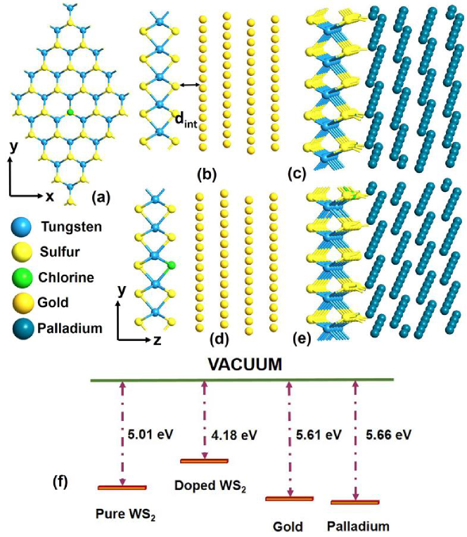
Figure 1 (a) shows the stable atomic structure of chlorine doped 5x5 supercell of WS2. We perform formation energy calculations to find the thermodynamically stable position for sulfur substitution by chlorine atoms with EForm values as 2.92 eV. This supercell is interfaced with 111 cleaved surface of Au and Pd respectively. While interfacing the lattice constant of WS2 is fixed and the metal slab is subjected to match with it. Figure 1 (c) and (d) shows the ball and stick model of the doped 5x5 WS2-Au and WS2-Pd interface. Total energy calculations reveal 2.7 Å and 2.2 Å as the equilibrium interlayer separation between the WS2 (pure and doped) with Au and Pd metal slabs. The binding energy values obtained per sulfur atom is -0.18 eV (pure) and -0.19 eV (doped) for gold and -0.39 eV (pure) and -0.4 eV (doped) for palladium respectively. We calculate the work function of pure and doped WS2 and metals Au and Pd and are shown in Figure 1(f).
Substitution by chlorine doping amounts to 2% of total sulfur atoms which leads to a very high doping concentration in 5x5 supercell of WS2. However, to realize the substitution by considering the experimental doping concentration value of 6 x 1011 cm-2 studied here Ref.(14), a much bigger supercell is required leading to further increase in computational burden. To reduce the computational cost and study the effect of doping on SBH reduction we limit ourselves with a 5x5 supercell.
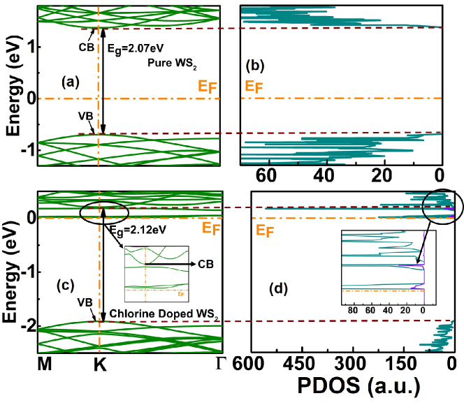
The electronic structures of both pure and doped WS2 along with the density of states are compared in Figure 2 to highlight the effect of doping. The band gap of pure WS2 is 2.07 eV. The positions of CB and Valence Band (VB) is verified with PDOS kept along the side of bandstructure. We see that substitution of single chlorine dopant shifts the energy bands towards the EF and creates midgap states in the vicinity of EF. The number of midgap states is 2 , one of which splits into two bands between the high symmetry points of brillouin zone shown in the inset of Figure 2 (c). The two mid gap states have significant contribution in the PDOS as well. The main contributor of these states is chlorine which is shown in inset of Figure 2 (d) with purple color. The energy level is 0.184 eV for the mid gap state near the conduction band minima (CBM). The splitting of bands leads to two energy levels 0.028 eV and 0.020 eV respectively. These defect states originate from the hybridization of the Cl 3p and the W 5d states. There exists one unpaired extra electron due to n-type doping by chlorine. As tungsten lies in the 6th period of periodic table, chlorine, which has an extra negative charge, leads to the energy splitting of W d-orbitals and thus contribute to an extra mid gap state. The band gap in doped WS2 is also different as compared to the pure supercell (by 0.05 eV), which is attributed to the hybridization and change in the atomic structure due to chlorine substitution.
We then perform simulations to evaluate the nature of contact formed with WS2 (pure and doped) with Au and Pd. The Schottky barrier height is assessed using the electronic structure and DOS of projected WS2. Valence electron density and charge density difference are used to estimate the charge transfer across the interface. The localisation of electrons at the WS2-metal interface is studied using the ELF.
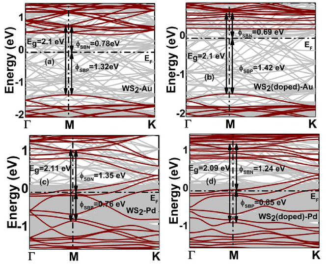
Both p-type and n-type SBH of projected WS2 (pure and doped) with Au and Pd are shown in Figure 3 (a)-(d). Since the interface involves two different atomic structures, the nature band gap is lost and projected band structure comprises of interface states. The origin of these states lies in the complex electronic hybridization occurring at the WS2-metal interface. Au is found to be physiosorped with WS2 where as Pd is chemisorped. Au, being an s-electron metal shows less hybridization as compared to Pd which is a d-electron metal and this effect is similar to MoS2-metal interfaceGong et al. (2014). The binding energy values quoted earlier confirm this nature. Moreover, the band gap regime also consists of less interface states in Au as compared to Pd (Figure 3 (a,c)).
For a pure WS2-Au interface, the amount of complexity in the bandstructure is less, but for a doped interface it is very high. This happens because the atoms in the doped supercell already hybridize with the substitutional impurity. The difference is visible in Figure 3 (b) and (d) with respect to Figure 3 (a) and (c). It further makes the determination of band gap edges difficult. However, density of states along with the electronic structure of projected WS2, can be used to identify the CBM and valence band maxima (VBM) as demonstrated in Ref.8 The difference between the CBM and VBM of all the interfaces differs from the band gap of pure WS2 by 0.04 eV. Strong interface hybridization causes emergence of more mid gap states for both the pure and doped supercells as visible in Figure 3 (c)-(d) for Pd due to its chemisorption nature with WS2. We observe that Au shows a n-type SBH and Pd shows p-type SBH when interfaced with WS2. The values of SBH are 0.78 eV and 0.76 eV respectively. In the complete band structure shown by grey lines, we see that the for Au the band lines are more dispersed in comparison to Pd. This indicates strong bonding of WS2 with Pd. Moreover, below the Fermi level, we see a complete metallization for Pd leading to the formation of p-type contact. Here, we see a similarity in the nature of contact between WS2 and WSe2 while forming an interface with Au and Pd.Kang et al. (2014) With the introduction of n-type impurity, the n-SBH exhibits a reduction for both metals. The n-SBH reduction attained is 0.09 eV for Au and 0.11 eV for Pd. We see the reduction in the n-SBH is higher for Pd in comparison to Au. Pd showing a p-type contact with WS2 also exhibits a reduction in the n-SBH and increase in p-SBH. This validates the observation that the chlorine is effective in reducing n-SBH for both the type of metals forming p-type and n-type SBH with WS2, and is equally competent for chemisorped and physiosorped metal interface with WS2. A slight variance in the band gap value of WS2 2.07 (for pure WS2 bandstructure) - 2.1 and 2.09 (projected WS2 bandstructure) is also observed due to heterogeneous atomic interface.
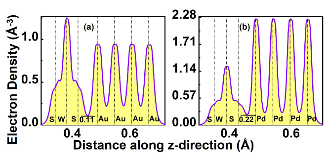
We also evaluate the valence electron density for WS2-metal interface as shown in Figure 4. The value of valence electron density is calculated as the minimum electron density at the metal-semiconductor interface. Higher values of electron density at the interface implies a better electron injection efficiency. The values with Au are for pure 0.10727 Å-3 and 0.10816 Å-3 for doped supercell. For pure and doped supercell with Pd they are 0.21888 Å-3 and 0.2212 Å-3 respectively. The high values for Pd indicate that more charge transfer has occurred when it is interfaced with WS2. Moreover the difference in the density values of doped and pure interface is higher for Pd as compared to Au.
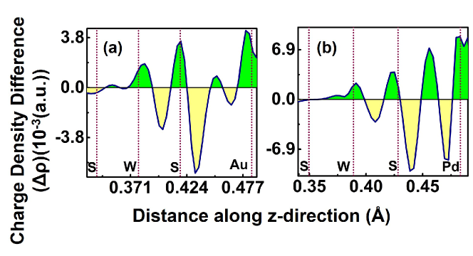
To substantiate the observations made in the above analysis, we examine the charge density difference of the respective geometries. Figure 5 shows the average charge density difference of WS2-metal interface for (a) Au and (b) Pd. A dipole gets created at the interface since both accumulation and depletion regions exist. Both the regions are shown by dissimilar colors to highlight the difference between them. At the junction between the nearest sulfur atom and metal atom, two peaks exist for depletion region and one peak for accumulation region. Moreover the accumulation shows a higher charge difference in Pd as compared to Au. A higher depletion regime implies that the charge carriers are repelled back from the surface and evinces a probability of least transmission across the interface. On the other hand, a higher accumulation regime implies that more charge is transferred across the interface. Hence we observe more hybridization for Pd rather than Au. The area calculated between the nearest S and metal atom using the methodology exhibited in Ref.8 is 0.03181 x 10⁻³ for Au and 0.06031 x 10⁻³ for Pd respectively and thus affirms the charge transfer is high for Pd. For pure and doped supercell-metal interface, the charge density difference curve shows a similar nature and the difference in areas for pure and doped case is higher for Pd. Because of this difference, a greater reduction on n-SBH is observed in Pd with respect to Au.
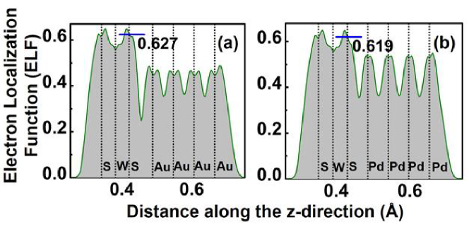
To study the localization of electrons at the WS2-metal interface, we study ELF which is dimensionless quantity. It is defined as the possibility of finding an electron in the neighborhood of a reference electron. Its value ranges from 0ELF1, with the maximum limit ELF=1 corresponding to prefect localization and ELF=0.5 corresponding to electron-gas like pair probabilityBecke and Edgecombe (1990). Figure 6 shows the value of ELF for WS2-Au and WS2-Pd interface. The value obtained for Pd is less in comparison to Au. This implies that Au is more localized than Pd indicating a better bonding for WS2-Pd interface.
It is interesting to note that for TMD channel based transistors, in a top contact device structure, two types of interfaces exist. One interface is between the TMD-metal and the other is between the TMD underneath the metal contact and TMD forming the channel (Kang et al., 2014). Here we find the SBH formed at the first interface. For calculating the SBH at the second interface, transport simulations need to be conducted along the device length. The effective SBH combining both the interfaces can then be determined using LDOS distribution. However, carrying transport simulations employing pseudopotentials with basis functions having higher orbital contribution requires powerful computing system, as the number of atoms increase manifold from bulk-configuration to device-configuration. Nevertheless while discussing SBH and the associated contact resistance in the context of ON current of the MOSFET, the gate current is kept high and the channel is inverted. In this condition, the CBM of the TMD channel region (not touching the metal) can be assumed to be lower than CBM of the other TMD regime. Hence, the SBH evaluated in this work can be considered as the effective SBH.
In the above study we investigate the contact nature of pure and Cl doped monolayer WS2 with Au111 and Pd111. First the electronic structures of pure and doped supercells are investigated. We find that band energies near to the conduction band edge align close to Fermi level with the formation of mid gap states and band splitting. Further, the pure and doped optimized supercell are adsorbed on the metals. Interface with pure supercell determines that Au is physiosorped with WS2 and has an n-type SBH while Pd is chemisorped with WS2 having a p-type SBH. Adsorption with Cl doped supercell shows a reduction of n-type SBH for both the metals. All the results are validated by studying charge redistribution at the WS2-metal interface. The above understandings may further contribute to explore other TMD-metal interfaces, as well as in investigating various possible dopants for chalcogenide substitution.
Acknowledgements.
The work was supported by Science Engineering and Research Board -Department of Science and Technology (SERB DST), Govt. of India, under Grant no. SR/S3/EECE/0151/2012. The authors would like to thank Quantumwise support staff for their useful discussions.References
- Radisavljevic et al. (2011) B. Radisavljevic, A. Radenovic, J. Brivio, V. Giacometti, and A. Kis, “Single-layer mos2 transistors,” Nature nanotechnology 6, 147–150 (2011).
- Sik Hwang et al. (2012) W. Sik Hwang, M. Remskar, R. Yan, V. Protasenko, K. Tahy, S. Doo Chae, P. Zhao, A. Konar, H. (Grace) Xing, A. Seabaugh, and D. Jena, “Transistors with chemically synthesized layered semiconductor ws2 exhibiting 105 room temperature modulation and ambipolar behavior,” Applied Physics Letters 101, 013107 (2012).
- Liu et al. (2014) X. Liu, J. Hu, C. Yue, N. D. Fera, Y. Ling, Z. Mao, and J. Wei, “High performance field-effect transistor based on multilayer tungsten disulfide,” ACS Nano 8, 10396–10402 (2014).
- Das and Appenzeller (2013) S. Das and J. Appenzeller, “Wse2 field effect transistors with enhanced ambipolar characteristics,” Applied Physics Letters 103, 103501 (2013).
- Larentis, Fallahazad, and Tutuc (2012) S. Larentis, B. Fallahazad, and E. Tutuc, “Field-effect transistors and intrinsic mobility in ultra-thin mose2 layers,” Applied Physics Letters 101, 223104 (2012).
- Pradhan et al. (2014) N. R. Pradhan, D. Rhodes, S. Feng, Y. Xin, S. Memaran, B.-H. Moon, H. Terrones, M. Terrones, and L. Balicas, “Field-effect transistors based on few-layered α-mote2,” ACS Nano 8, 5911–5920 (2014).
- Leong et al. (2014) W. S. Leong, X. Luo, Y. Li, K. H. Khoo, S. Y. Quek, and J. T. Thong, “Low resistance metal contacts to mos2 devices with nickel-etched-graphene electrodes,” ACS nano 9, 869–877 (2014).
- Chanana and Mahapatra (2015) A. Chanana and S. Mahapatra, “Theoretical insights to niobium-doped monolayer mos2 gold contact,” Electron Devices, IEEE Transactions on 62, 2346–2351 (2015).
- Das et al. (2013) S. Das, H.-Y. Chen, A. V. Penumatcha, and J. Appenzeller, “High performance multilayer mos2 transistors with scandium contacts,” Nano Letters 13, 100–105 (2013).
- Kang, Liu, and Banerjee (2014) J. Kang, W. Liu, and K. Banerjee, “High-performance mos2 transistors with low-resistance molybdenum contacts,” Applied Physics Letters 104, 093106 (2014).
- Laskar et al. (2014) M. R. Laskar, D. N. Nath, L. Ma, E. W. Lee II, C. H. Lee, T. Kent, Z. Yang, R. Mishra, M. A. Roldan, J.-C. Idrobo, et al., “P-type doping of mos2 thin films using nb,” Applied Physics Letters 104, 092104 (2014).
- Suh et al. (2014) J. Suh, T.-E. Park, D.-Y. Lin, D. Fu, J. Park, H. J. Jung, Y. Chen, C. Ko, C. Jang, Y. Sun, R. Sinclair, J. Chang, S. Tongay, and J. Wu, “Doping against the native propensity of mos2: Degenerate hole doping by cation substitution,” Nano Letters 14, 6976–6982 (2014).
- Liu et al. (2011) L. Liu, S. Bala Kumar, Y. Ouyang, and J. Guo, “Performance limits of monolayer transition metal dichalcogenide transistors,” Electron Devices, IEEE Transactions on 58, 3042–3047 (2011).
- Yang et al. (2014) L. Yang, K. Majumdar, H. Liu, Y. Du, H. Wu, M. Hatzistergos, P. Y. Hung, R. Tieckelmann, W. Tsai, C. Hobbs, and P. D. Ye, “Chloride molecular doping technique on 2d materials: Ws2 and mos2,” Nano Letters 14, 6275–6280 (2014).
- Khomyakov et al. (2009) P. A. Khomyakov, G. Giovannetti, P. C. Rusu, G. Brocks, J. van den Brink, and P. J. Kelly, “First-principles study of the interaction and charge transfer between graphene and metals,” Phys. Rev. B 79, 195425 (2009).
- Gong et al. (2010) C. Gong, G. Lee, B. Shan, E. M. Vogel, R. M. Wallace, and K. Cho, “First-principles study of metal–graphene interfaces,” Journal of Applied Physics 108, – (2010).
- Popov, Seifert, and Tománek (2012) I. Popov, G. Seifert, and D. Tománek, “Designing electrical contacts to monolayers: A computational study,” Phys. Rev. Lett. 108, 156802 (2012).
- Kang et al. (2014) J. Kang, W. Liu, D. Sarkar, D. Jena, and K. Banerjee, “Computational study of metal contacts to monolayer transition-metal dichalcogenide semiconductors,” Phys. Rev. X 4, 031005 (2014).
- (19) “Atomistix ToolKit v.15.beta Quantumwise ,” http://quantumwise.com/.
- Perdew and Zunger (1981) J. P. Perdew and A. Zunger, “Self-interaction correction to density-functional approximations for many-electron systems,” Phys. Rev. B 23, 5048–5079 (1981).
- Hartwigsen, Goedecker, and Hutter (1998) C. Hartwigsen, S. Goedecker, and J. Hutter, “Relativistic separable dual-space gaussian pseudopotentials from h to rn,” Phys. Rev. B 58, 3641–3662 (1998).
- Monkhorst and Pack (1976) H. J. Monkhorst and J. D. Pack, “Special points for brillouin-zone integrations,” Physical Review B 13, 5188 (1976).
- Jiang (2012) H. Jiang, “Electronic band structures of molybdenum and tungsten dichalcogenides by the gw approach,” The Journal of Physical Chemistry C 116, 7664–7671 (2012).
- Kumar and Ahluwalia (2012) A. Kumar and P. Ahluwalia, “Electronic structure of transition metal dichalcogenides monolayers 1h-mx2 (m= mo, w; x= s, se, te) from ab-initio theory: new direct band gap semiconductors,” The European Physical Journal B 85, 1–7 (2012).
- Dolui et al. (2013) K. Dolui, I. Rungger, C. Das Pemmaraju, and S. Sanvito, “Possible doping strategies for mos2 monolayers: An ab initio study,” Phys. Rev. B 88, 075420 (2013).
- Van de Walle and Neugebauer (2004) C. G. Van de Walle and J. Neugebauer, “First-principles calculations for defects and impurities: Applications to iii-nitrides,” Journal of Applied Physics 95, 3851–3879 (2004).
- Gong et al. (2014) C. Gong, L. Colombo, R. M. Wallace, and K. Cho, “The unusual mechanism of partial fermi level pinning at metal–mos2 interfaces,” Nano letters 14, 1714–1720 (2014).
- Becke and Edgecombe (1990) a. D. Becke and K. E. Edgecombe, “A simple measure of electron localization in atomic and molecular systems,” J. Chem. Phys. 92, 5397 (1990).