Ballistic Josephson junctions in edge-contacted graphene
Hybrid graphene-superconductor devices have attracted much attention since the early days of graphene research[1, 2, 3, 4, 5, 6, 7, 8, 9, 10, 11, 12, 13, 14, 15, 16, 17, 18]. So far, these studies have been limited to the case of diffusive transport through graphene with poorly defined and modest quality graphene-superconductor interfaces, usually combined with small critical magnetic fields of the superconducting electrodes. Here we report graphene based Josephson junctions with one-dimensional edge contacts[19] of Molybdenum Rhenium. The contacts exhibit a well defined, transparent interface to the graphene, have a critical magnetic field of 8 Tesla at 4 Kelvin and the graphene has a high quality due to its encapsulation in hexagonal boron nitride[20, 19]. This allows us to study and exploit graphene Josephson junctions in a new regime, characterized by ballistic transport. We find that the critical current oscillates with the carrier density due to phase coherent interference of the electrons and holes that carry the supercurrent caused by the formation of a Fabry-Pérot cavity. Furthermore, relatively large supercurrents are observed over unprecedented long distances of up to 1.5 m. Finally, in the quantum Hall regime we observe broken symmetry states while the contacts remain superconducting. These achievements open up new avenues to exploit the Dirac nature of graphene in interaction with the superconducting state.
In particular, the chiral nature of the charge carriers in graphene is predicted to give rise to specular Andreev reflection [21], and the conventional quantum Hall effect can be markedly different due to the interaction between edge states and the superconductor[22, 23]. Such systems also provide a unique way to probe valley-polarized edge states[24], topological confinement in bilayer graphene [25], the interplay between superconductivity and quantum confinement or ballistic two-dimensional Josephson junctions and their response to phase coherent interference effects.
There are two important prerequisites that must be satisfied in order to observe any of these phenomena experimentally. First, the graphene-superconductor interface should be transparent and well defined. Secondly, the graphene must be of high electronic quality. In addition, for some of the above effects, a superconductor with a large upper critical field, , is required. While significant technological progress has been made in improving the quality of graphene by either suspending graphene[26] or encapsulating it in hexagonal boron nitride (hBN) [20, 19], the main challenge has been to combine such low-scattering graphene with a (large ) superconductor. All reports on graphene-superconductor devices to date involved superconducting contacts deposited directly on the graphene surface, and diffusive transport through the device. In addition to the modest electronic quality, the use of top contacts leaves ambiguity in where exactly Andreev reflection takes place and under what spectral conditions. I.e. it is not clear how far electrons travel beneath the contact before entering the superconductor.
To realise high quality graphene-superconductor junctions we encapsulate graphene between two hBN crystals using the van der Waals pick-up method [19]. This method ensures that the graphene is never in contact with any polymer during the stacking and thereafter. Electrical contact is made by metal deposition onto areas where the stack has been etched through. Unlike earlier work[19], where metal deposition is done in a separate lithography step, we start by etching only the region to be contacted, followed immediately by metal deposition. This has the following advantages: (i) our contacts are self-aligned, thereby minimizing redundant metal overlap above the graphene and reducing the screening of electric and magnetic fields and (ii) combining the etching and deposition in one step minimizes resist residues at the contact interface, which is necessary for transparent contacts. Instead of a normal metal, we sputter an alloy superconductor MoRe, which is attractive in several respects. First, MoRe is a type-II superconductor with a critical temperature K and an upper critical field T (at 4.2 K), which should easily allow for the observation of quantum Hall states while the MoRe remains predominantly superconducting. Secondly, it has been shown that MoRe makes good electrical contact to carbon-based materials such as carbon nanotubes [27]. Considering the fact that edge-contact resistance can vary by an order of magnitude depending on the choice of metal [19], it is critical to select a superconductor which makes good electrical contact to graphene. This is particularly important in the context of superconductor (S) graphene (G) JJs, where the transparency of the S-G interface directly affects the Andreev reflection. Furthermore, unlike surface contacts, such one-dimensional edge contacts ensure that the Andreev reflection occurs at a well-defined location, at the edge of the graphene, where it contacts with the 3-dimensional bulk superconductor. After the deposition of the superconducting electrodes, we etch the stack into the desired geometry.
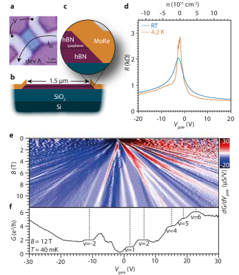
An optical image and a cross-sectional schematic of device are shown in Fig. 1a-c. The graphene is etched to a long and wide rectangle, with MoRe edge contacts on either side. All measurements described here are performed in a (dc) four point geometry, as shown in Fig. 1a. The MoRe leads are arranged such that the lead series resistance is minimized and the measured resistance is effectively the two-probe graphene resistance, irrespective of whether the MoRe is normal or superconducting. This is important since disordered superconductors such as MoRe have a large normal-state resistivity, potentially confusing the interpretation of the measurements when the electrodes turn normal (see SI).
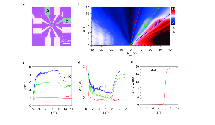
Fig. 1d shows the measured resistance, , versus back gate voltage, , at room temperature and 4.2 K. A clear electron-hole asymmetry is visible with the resistance in the hole doped () regime being somewhat larger than that in the electron doped () regime. We attribute this to contact-induced -type doping, which leads to the formation of junctions close to the contacts when the bulk of the graphene is doped. Such type doping effects from normal edge contacts have also recently been reported [28]. Fig. 1e shows the Landau fan diagram recorded up to . The high electronic quality of the graphene is evident from the emergence of broken symmetry states above , which are well developed at (Fig. 1f). To our knowledge, this is the first observation of broken symmetry states in graphene with superconducting contacts. The plateaus on the electron side are better developed than those on the hole side, presumably a consequence of doping near the contacts.
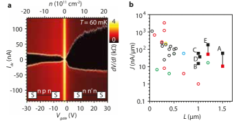
At zero magnetic field we observe a gate-tunable supercurrent through the device. In Fig. 2a we plot the diffential resistance, , as a function of gate voltage, , and the current bias, . Evidently, the critical current, , vanishes at the charge neutrality point, but reaches values in excess of 100 nA at V V. The individual curves are hysteretic, as is evident from the asymmetry about (we discuss the possible origins of this hysteresis in the SI). On the hole side is considerably smaller, consistent with the formation of the conjectured junctions. In Fig. 2b we plot the critical current density per unit length, , versus the JJ length, , with data obtained from previous reports of graphene JJs (circles) along with the present MoRe edge-contacted devices (squares). The black squares show the critical current density at , whereas the red squares are taken at . We point out that the critical current density depends on the temperature and the graphene carrier density, which vary from study to study. Despite this, it is clear that our MoRe edge-contacted devices stand out in relative magnitude compared to the previous data. We find large supercurrent densities (up to ) over significantly longer distances (). The observation of large supercurrents over an unprecedented long distance of 1.5 indicates a high quality of both the graphene itself and of the 1D graphene-superconductor interfaces.
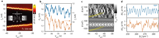
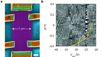
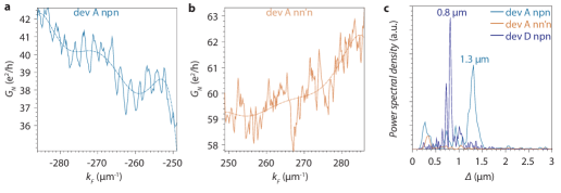
In addition, we find unambiguous signatures of ballistic Josephson transport in this 2D geometry. As shown in Fig. 3a, we observe for the first time clear oscillations in the critical current and the retrapping current when we vary the gate voltage, indicative of Fabry-Pérot (FP) interferences in the supercurrent through the junction. The transmission probability of electrons and holes that carry the supercurrent is the result of interference of trajectories that travel ballistically from one contact to the other with multiple reflections close to or at the edges of the graphene flake. As the gate voltage is varied, the Fermi wavelength changes, constructive and destructive interference alternate, leading to modulations in the critical current. One may expect the graphene-superconductor interfaces to form the walls of the cavity. However, we observe the oscillations only on the hole-doped side and not on the electron-doped side (see Fig. 3d and the discussion below). This suggests that in the presence of -doped regions near the MoRe-graphene interface the relevant cavity is instead formed by junctions near the contacts (see inset Fig. 3a). This gives rise to a reduced cavity length . This length can be directly inferred from the period of the oscillations, extracted via a Fourier analysis (see SI) of these oscillations over many periods. A cavity length of is found, which is smaller than the etched device length (). A similar difference between device size and inferred cavity length was seen in device (see SI). This difference may arise from screening of the back gate near the contacts in combination with the presence of the n-doped regions at the MoRe-graphene interfaces in both devices.
The interpretation of the oscillations in in terms of FP interference, is further supported by comparing them with the oscillations in the normal state conductance, , measured at currents just above . The oscillations of with gate voltage clearly match the oscillations in , (see Fig. 3b), as expected for Josephson junctions. In the case of normal state transport, we can apply a weak magnetic field perpendicular to the graphene, to apply a Lorentz force to the trajectories of electrons and holes. This is expected to give a characteristic shift of the FP resonances due to the accumulation of extra field-dependent phases. Indeed in the measurements shown in Fig. 3c, we find that as B increases the main resonance features shift to higher density, following a characteristic dispersion. To enhance the visibility, we plot the quantity , which was obtained after subtracting a gate dependent (but field independent) modulation of the background conductance. We compare the data with the results of numerical simulations of the device conductance (see methods for further details) in the ballistic regime and with junctions for the exact geometry of the measured device (Fig. 3c lower panel). Simulation and experiment show an almost identical dispersion of the FP resonances with magnetic field. It is also possible to obtain a semiclassical expression for the resonance condition (see SI) by considering all the phases accumulated in the n-region of the junction:
| (1) |
with a specific integer mode, the Fermi wavelength which is tuned by the backgate (), the cavity size, the electron charge and Planck’s constant. The yellow curves in Fig. 3d are calculated using Eq. 1 for modes and show an excellent agreement with the measured and simulated results. This provides strong evidence that the observed oscillations, both in and , arise from Fabry-Pérot interference, which implies phase-coherent ballistic transport. While such oscillations due to FP interference have been reported before in a variety of systems including high-quality graphene with normal contacts [2, 30], here we provide evidence for phase coherent FP interference in the supercurrent, which has not been observed before in any 2D geometry.
In order to better understand the microscopic details of our device, we compare the conductance in the regime with that in the regime (Fig. 3d). Whereas in the regime (upper panel), we observe periodic oscillations as a function of absolute wave number, , we observe universal conductance fluctuations (UCF) in the case (lower panel). We attribute these fluctuations to diffuse boundary scattering at or close to the graphene-MoRe interface. This diffuse scattering should also be present on the hole-side but does not dominate the transport due to the presence of the junctions. Using the ballistic limit, much larger than the mean free path, where all resistance is from the contact interface, we can estimate a lower bound on the contact transparency, via . From the conductance in the regime (see SI) we find a contact transparency of . In the case, the conductance is dominated by the barriers. In this case, we can estimate the sharpness, , of the to transition regions via . We find a sharpness of , which is a plausible value considering the device dimensions.
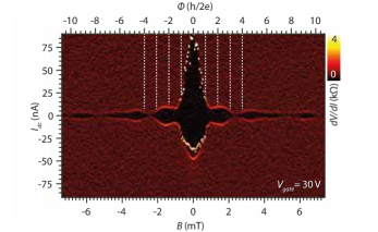
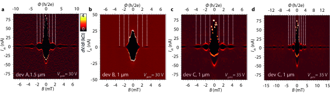
Since the DC Josephson effect is observed in these graphene devices over micron scale distances, we can also explore the magnetic field dependence of the critical current for unusual geometries. Earlier reports concerned graphene Josephson junctions with lengths much shorter than their width. In this case, the magnetic field dependence of is expected to follow the standard Fraunhofer diffraction pattern observed in tunnel junctions[31]. In the present devices, in contrast, the aspect ratio is close to 1, which has two consequences. First, unlike in tunnel junctions, the phase difference across the junction must be integrated along both interfaces. Furthermore, contributions involving reflections off the side of the junction must be included, especially when transport is ballistic[32, 33, 34]. The main prediction in this case is that the periodicity of with magnetic flux becomes larger than a single flux quantum, . Despite significant differences across the patterns measured on the various devices, we consistently find a period larger than , as seen in Fig. 4 for device (and in the SI for devices and ). In contrast, earlier reports on graphene Josephson junctions all show flux periods smaller than [1, 2, 5, 7, 16, 9, 12, 13] before corrections to account for the London penetration depth.
The Fabry Pérot oscillations in the critical current and the anomalous Fraunhofer diffraction patterns are mutually consistent and provide strong evidence of ballistic effects in superconducting transport through graphene. We believe that this is the first unambiguous demonstration of a ballistic JJ in graphene.
.1 Methods
.1.1 DC transport measurements
Low temperature dc measurements are done in a Leiden Cryogenics MCK-50 dilution fridge. The setup can reach a base temperature of 40 mK with an electron temperature of about 70 mK. DC Currents and voltages are applied and probed with a home-built measurement setup. Furthermore the setup is equipped with a superconducting magnet coil that can sustain fields of up to 12 T.
.1.2 Tight-binding simulation
The FP oscillations in the junction are simulated by a tight-binding calculation using the Kwant software package[35]. The source code has been provided along with this submission as an ancillary file. A hexagonal lattice is discretized with a lattice constant of , with metallic leads on the wide sides. The contact induced doping near both leads is modeled by a region with a fixed chemical potential. The width of the transition region from the to the central region is set to and modelled by . A finite contact resistance is imposed by reducing the transparency between the central strip and the leads to . Finally we calculate the transmission as a function of the Fermi wavenumber and magnetic field , resulting in the dispersion given in Fig. 3d.
.2 Acknowledgements
We thank Vibhor Singh for sharing the MoRe sputtering recipe and Carlo Beenakker for fruitful discussions. We acknowledge support from the EC-FET Graphene Flagship, from the European Research Council Advanced grant No. 339306 (METIQUM), from a European Research Council Synergy grant (QC-LAB), and from the Ministry of Education and Science of the Russian Federation under Contract No. 14.B25.31.0007. This work is part of the Nanofront consortium, funded by the Dutch Science Foundation OCW/NWO/FOM.
.3 Author contributions
K.W. and T.T. grew the hBN crystals, G.N. fabricated the devices, V.E.C. and S.G. performed the measurements, and M.D. and A.R.A. did the numerical simulations and theory. The measurements were analyzed and interpreted by V.E.C, S.G., M.D, A.R.A, T.M.K., and L.M.K.V. The manuscript was written by V.E.C, S.G. and L.M.K.V. with input from A.R.A., M.D. and T.M.K.
The authors declare no competing financial interests.
References
- [1] Hubert B. Heersche, Pablo Jarillo-Herrero, Jeroen B. Oostinga, Lieven M K. Vandersypen, and Alberto F. Morpurgo. Bipolar supercurrent in graphene. Nature (London), 446:56–59, 2007.
- [2] Xu Du, Ivan Skachko, and Eva Y. Andrei. Josephson current and multiple Andreev reflections in graphene SNS junctions. Phys. Rev. B, 77:184507, 2008.
- [3] Feng Miao, Wenzhong Bao, Hang Zhang, and Chun Ning Lau. Premature switching in graphene Josephson transistors. Solid State Commun., 149:1046 – 1049, 2009.
- [4] C. Girit, V. Bouchiat, O. Naaman, Y. Zhang, M. F. Crommie, A. Zettl, and I. Siddiqi. Tunable graphene dc superconducting quantum interference device. Nano Lett., 9:198–199, 2009.
- [5] C. Ojeda-Aristizabal, M. Ferrier, S. Guéron, and H. Bouchiat. Tuning the proximity effect in a superconductor-graphene-superconductor junction. Phys. Rev. B, 79:165436, 2009.
- [6] A. Kanda, T. Sato, H. Goto, H. Tomori, S. Takana, Y. Ootuka, and K. Tsukagoshi. Dependence of proximity-induced supercurrent on junction length in multilayer-graphene Josephson junctions. Phys. C (Amsterdam, Neth.), 470:1477 – 1480, 2010.
- [7] Jae-Hyun Choi, Hu-Jong Lee, and Yong-Joo Doh. Above-gap conductance anomaly studied in superconductor-graphene-superconductor Josephson junctions. J. Korean Phys. Soc., 57:149, 2010.
- [8] I. V. Borzenets, U. C. Coskun, S. J. Jones, and G. Finkelstein. Phase diffusion in graphene-based Josephson junctions. Phys. Rev. Lett., 107:137005, 2011.
- [9] U. C. Coskun, M. Brenner, T. Hymel, V. Vakaryuk, A. Levchenko, and A. Bezryadin. Distribution of supercurrent switching in graphene under proximity effect. Phys. Rev. Lett., 108:097003, 2012.
- [10] Gil-Ho Lee, Dongchan Jeong, Jae-Hyun Choi, Yong-Joo Doh, and Hu-Jong Lee. Electrically tunable macroscopic quantum tunneling in a graphene-based Josephson junction. Phys. Rev. Lett., 107:146605, 2011.
- [11] Peter Rickhaus, Markus Weiss, Laurent Marot, and Christian Schönenberger. Quantum Hall effect in graphene with superconducting electrodes. Nano Lett., 12:1942–1945, 2012.
- [12] M. Popinciuc, V. E. Calado, X. L. Liu, A. R. Akhmerov, T. M. Klapwijk, and L. M. K. Vandersypen. Zero-bias conductance peak and Josephson effect in graphene-NbTiN junctions. Phys. Rev. B, 85(20):205404–, 2012.
- [13] Katsuyoshi Komatsu, Chuan Li, S. Autier-Laurent, H. Bouchiat, and S. Gueron. Superconducting proximity effect through graphene from zero field to the quantum Hall regime. Phys. Rev. B, 86:115412, 2012.
- [14] Naomi Mizuno, Bent Nielsen, and Xu Du. Ballistic-like supercurrent in suspended graphene Josephson weak links. Nat. Commun., 4:–, 2013.
- [15] Juha Voutilainen, Aurelien Fay, Pasi Häkkinen, Janne K. Viljas, Tero T. Heikkilä, and Pertti J. Hakonen. Energy relaxation in graphene and its measurement with supercurrent. arXiv:1103.3234 [cond-mat.mes-hall], 2011.
- [16] Dongchan Jeong, Jae-Hyun Choi, Gil-Ho Lee, Sanghyun Jo, Yong-Joo Doh, and Hu-Jong Lee. Observation of supercurrent in PbIn-graphene-PbIn Josephson junction. Phys. Rev. B, 83:094503, Mar 2011.
- [17] I. V. Borzenets, U. C. Coskun, H. T. Mebrahtu, Yu. V. Bomze, A. I. Smirnov, and G. Finkelstein. Phonon bottleneck in graphene-based Josephson junctions at millikelvin temperatures. Phys. Rev. Lett., 111:027001, Jul 2013.
- [18] Jae-Hyun Choi, Gil-Ho Lee, Sunghun Park, Dongchan Jeong, Jeong-O Lee, H.-S. Sim, Yong-Joo Doh, and Hu-Jong Lee. Complete gate control of supercurrent in graphene p–n junctions. Nat Commun, 4:–, 2013.
- [19] L. Wang, I. Meric, P. Y. Huang, Q. Gao, Y. Gao, H. Tran, T. Taniguchi, K. Watanabe, L. M. Campos, D. A. Muller, J. Guo, P. Kim, J. Hone, K. L. Shepard, and C. R. Dean. One-dimensional electrical contact to a two-dimensional material. Science, 342(6158):614, 2013.
- [20] C.R. Dean, A.F. Young, I. Meric, C. Lee, L. Wang, S. Sorgenfrei, K. Watanabe, T. Taniguchi, P. Kim, K.L. Shepard, and J. Hone. Boron nitride substrates for high-quality graphene electronics. Nat. Nanotech., 5:722–726, 2010.
- [21] C W J. Beenakker. Specular Andreev reflection in graphene. Phys. Rev. Lett., 97:067007, 2006.
- [22] H. Hoppe, U. Zülicke, and Gerd Schön. Andreev reflection in strong magnetic fields. Phys. Rev. Lett., 84:1804–1807, 2000.
- [23] N. M. Chtchelkatchev and I. S. Burmistrov. Conductance oscillations with magnetic field of a two-dimensional electron gas - superconductor junction. Phys. Rev. B, 75:214510, 2007.
- [24] A. R. Akhmerov and C. W. J. Beenakker. Detection of valley polarization in graphene by a superconducting contact. Phys. Rev. Lett., 98:157003, Apr 2007.
- [25] Ivar Martin, Ya. M. Blanter, and A. F. Morpurgo. Topological confinement in bilayer graphene. Phys. Rev. Lett., 100:036804, 2008.
- [26] Xu Du, Ivan Skachko, Anthony Barker, and Eva Y. Andrei. Approaching ballistic transport in suspended graphene. Nat. Nanotech., 3:491–495, 2008.
- [27] B. H. Schneider, S. Etaki, H. S. J. van der Zant, and G. A. Steele. Coupling carbon nanotube mechanics to a superconducting circuit. Sci. Rep., 2:599, September 2012.
- [28] Patrick Maher, Lei Wang, Yuanda Gao, Carlos Forsythe, Takashi Taniguchi, Kenji Watanabe, Dmitry Abanin, Zlatko Papić, Paul Cadden-Zimansky, James Hone, Philip Kim, and Cory R. Dean. Tunable fractional quantum Hall phases in bilayer graphene. Science, 345(6192):61–64, July 2014.
- [29] Andrea F. Young and Philip Kim. Quantum interference and Klein tunnelling in graphene heterojunctions. Nat. Phys., 5:222–226, 2009.
- [30] Anastasia Varlet, Ming-Hao Liu, Viktor Krueckl, Dominik Bischoff, Pauline Simonet, Kenji Watanabe, Takashi Taniguchi, Klaus Richter, Klaus Ensslin, and Thomas Ihn. Fabry-Pérot interference in gapped bilayer graphene with broken anti-Klein tunneling. Phys. Rev. Lett., 113:116601, Sep 2014.
- [31] Michael Tinkham. Introduction to superconductivity. Dover, New York, 2nd edition, 2004.
- [32] J. P. Heida, B. J. van Wees, T. M. Klapwijk, and G. Borghs. Nonlocal supercurrent in mesoscopic Josephson junctions. Phys. Rev. B, 57(10):R5618–R5621, 1998.
- [33] Urs Ledermann, Alban L. Fauchère, and Gianni Blatter. Nonlocality in mesoscopic Josephson junctions with strip geometry. Phys. Rev. B, 59:R9027–R9030, 1999.
- [34] Daniel E. Sheehy and Alexandre M. Zagoskin. Theory of anomalous magnetic interference pattern in mesoscopic superconducting/normal/superconducting Josephson junctions. Phys. Rev. B, 68(14):144514–, October 2003.
- [35] Christoph W Groth, Michael Wimmer, Anton R Akhmerov, and Xavier Waintal. Kwant: a software package for quantum transport. New J. Phys., 16(6):063065–, 2014.
I Supplementary Information
V. E. Calado S. Goswami G. Nanda M. Diez A. R. Akhmerov K. Watanabe T. Taniguchi T. M. Klapwijk L. M. K. Vandersypen
II Device fabrication
Graphene flakes are mechanically exfoliated from natural graphite (NGS naturgraphit GmbH) with blue Nitto tape (SWT 20+ Nitto Dekko Corp.) and put on Si substrates with a 90 nm thick thermally grown SiO2 top layer (IDB technologies Ltd.). Single layer graphene is located under an optical microscope (Olympus BX51). The bottom hexagonal Boron Nitride (hBN) flakes are made in the same way as the graphene flakes, using substrates with 285 nm thermally SiO2 (NOVA Electronic Materials, LLC). The top hBN flakes are prepared on polymer coated transparent substrates. The transparent substrates consist of a microscope glass slide with a PDMS (Polydimethylsiloxane) film(GelPak, WF-40-X4-A). On top of that we spin (1500 RPM for 55 sec) 9 wt% MMA (Methylmethacrylate) in Ethyl lactate and bake it for 20 min at 120 ∘C. The MMA film acts as a transfer agent and the PDMS film promotes a cushioning effect during the pickup and transfer. The glass slide with hBN flakes is mounted in a micromanipulator. The setup is similar to that of ref. [1] but with an additional heating stage implemented. The graphene on Si/SiO2 substrate is heated to about and brought in contact with the top hBN. The MMA becomes soft and the graphene is picked up through adhesion to the hBN. Subsequent transfer is done at a higher temperature of . The stack is patterned using standard E-beam lithography with a thick PMMA mask and is shaped by reactive ion etching in a O2 plasma during 1 min (Leybold-Heraeus, 60 W, ) and subsequently in a CHF3 /O2 plasma during 1 min (60 W, ). Next 80 nm MoRe is deposited by a sputtering process using a DC plasma with a power of 100 W in Ar. Lift-off is completed in hot acetone () for about 3-4 hours. A second lithography step defines the intended graphene geometry in a PMMA / hydrogen silsesquioxane (HSQ) mask, followed by an etch step using the same plasma conditions as in the first lithography step. The fabricated devices are not exposed to any (Ar/H2) annealing processes that are common for graphene devices.
III Details on the -junction semiclassics
In Fig. 3c of the main text we have highlighted the dispersion of dominant Fabry Pérot resonances with the external magnetic field. Here we derive these resonances from the semiclassical phase accumulated in the -region of the -junction. If the junction is along the -direction the total Landauer conductance of the junction can be expressed as a sum of transmission amplitudes over transverse momenta . The leading contribution of the oscillating part of the conductance is given by [2]
| (2) |
Here is the length of the -doped region (the cavity), the mean-free path in the -region. Choosing the center of the junction at and using the Landau gauge where , the transmission and reflection amplitudes at the junctions located at are
| (3) |
and . Finally
| (4) |
is the semiclassical phase difference across the cavity for neighboring trajectories. For simplicity we have assumed that the junctions at are sharp. We are interested in resonances at finite fields where the transmission is dominated by small transverse momenta (see below) which acquire an additional nontrivial phase, up on reflection from the -junction. The total accumulated phase across the cavity and back is . At zero magnetic field is equivalent to normal incidence yielding a perfect transmission (Eq. (3)) and a vanishing contribution to the interference. In this regime the dominant contribution to the Fabry-Pérot resonances stems from finite momenta. The bending of the semiclassical trajectories due to the cyclotron motion at finite field causes a switch in the dominant contribution of the conductance to small momenta. The transition is characterized by a phase shift in the conductance oscillations at [2]
| (5) |
For fields larger than the characteristic field the largest contribution to the total conductance Eq. (2) is from ( is maximized by ). The switching field dependents on the degree of collimation at the -junctions which is determined by the electrical field , where across the junction. An estimate for the junction thickness is given in the main text. Unfortunately it is not possible for us to get a reliable estimate of the doping level in the n-doped region near the contacts. We observe -junction behavior up to very large negative back gate voltages. This suggest that screening from the contacts plays an important role in the local density level and profile rendering even a crude estimate on simple grounds impossible. From our experimental measurements we estimate the switching field to be below . This implies that the local electric field should be on the order of or smaller. The field range studied in Fig. 3c is well above this switching field allowing us to focus on the regime where the contribution to the conductance oscillations dominates. This contribution is resonant when the total acquired phase for is an integer multiple of
| (6) |
For small fields where the cyclotron radius is larger than the junction length we can expand to lowest order in
| (7) |
Using and we obtain a cyclotron radius . This confirms that our experiments are still in this regime. Finally from the resonance condition equation (6) we find
| (8) |
References
- [1] Andres Castellanos-Gomez, Michele Buscema, Rianda Molenaar, Vibhor Singh, Laurens Janssen, Herre S. J. van der Zant, and Gary A. Steele. Deterministic transfer of two-dimensional materials by all-dry viscoelastic stamping. 2D Materials, 1(1):011002, 2014.
- [2] Andrea F. Young and Philip Kim. Quantum interference and Klein tunnelling in graphene heterojunctions. Nat. Phys., 5:222–226, 2009.