Mreferences \newcitesSreferences_supplement
1 minute parity lifetime of a NbTiN Cooper-pair transistor
The parity modulation of the ground state of a superconducting island is a direct consequence of the presence of the Cooper pair condensate preferring an even number of charge carriers \citeMPhysRevLett.69.1993, Lafarge1993. The addition energy of an odd, unpaired quasiparticle equals to the superconducting gap, , suppressing single electron hopping in the low temperature limit, . Controlling the quasiparticle occupation is of fundamental importance for superconducting qubits as single electron tunneling results in decoherence \citeMClarke2008, Riste2013. In particular, topological quantum computation relies on the parity control and readout of Majorana bound states \citeM0034-4885-75-7-076501, read2012. Here we present parity modulation for the first time of a niobium titanite nitride (NbTiN) Cooper-pair transistor coupled to aluminium (Al) leads. We show that this circuit is compatible with the magnetic field requirement mT of inducing topological superconductivity in spin-orbit coupled nanowires \citeMPhysRevLett.105.077001, PhysRevLett.105.177002, Mourik25052012. Our observed parity lifetime exceeding 1 minute is several orders of magnitude higher than the required gate time of flux-controlled braiding of Majorana states \citeMPhysRevB.88.035121. Our findings readily demonstrate that a NbTiN island can be parity-controlled and therefore provides a good platform for superconducting coherent circuits operating in a magnetic field.
Experimentally, the parity modulation of a superconducting island can be observed via the ground state charge \citeMLafarge1993, the even-odd modulation of the charge stability diagram \citeMPhysRevLett.69.1997, PhysRevLett.70.1862, or the parity dependence of the switching current, \citeMPhysRevLett.72.2458. The interplay of the charging energy and the Josephson coupling makes the Cooper-pair transistor (CPT) a single, gate-modulated Josephson junction \citeMPhysRevLett.65.377, PhysRevLett.72.2458 with a 2e charge periodicity in the absence of parity switches, i.e. infinitely long parity lifetime, .
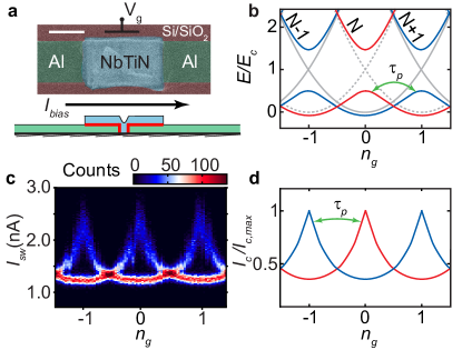
Recent, direct measurements of \citeMPhysRevB.78.024503, Riste2013 yielded values up to the millisecond regime for aluminium devices. Despite considerable efforts, however, no 2e periodicity has been reported for non-aluminium superconductors \citeMDolata2005, Savin2007, PhysRevB.76.172505, such as niobium or vanadium. Comparative studies of aluminium and niobium CPTs suggested that the elusiveness of parity effects is related to the material properties \citeMSavin2007, in accordance with earlier measurements showing that subgap quasiparticle states may appear in niobium due to oxidization of the bulk material \citeMHalbritter1987. In contrast, nitridized niobium compounds, such as niobium titanite nitride (NbTiN), have been shown to be less prone to form oxides and hence are good candidates for parity-conserving superconducting circuits. Furthermore, NbTiN forms transparent contacts with spin-orbit coupled semiconductor nanowires \citeMMourik25052012, and has become a preferred superconductor to investigate Majorana bound states.
Our device features a NbTiN island sputtered onto Al leads (Fig. 1a). The tunnel barriers between the island and the leads are created by means of controlled in-situ surface oxidization of Al, resulting in amorphous AlOx barriers \citeMOliver2013.
We extract a charging energy eV from the measured charge stability diagram. For different devices, we estimate eV from the superconducting gaps and normal state resistances of the junctions \citeMPhysRevLett.10.486 assuming equal resistances for the two tunnel barriers. A detailed list of parameters and characterization methods are presented in the supplementary material. Our devices are in the intermediate coupling regime with , where the energy diagram (Fig. 1b) and the critical current (Fig. 1d) are sensitive to the charge parity. It is important to note that our CPTs are in the optimal regime to establish flux-controlled braiding of Majorana bound states with \citeMPhysRevB.88.035121 and hence a useful platform to establish the parity lifetime for Majorana circuits \citeMPhysRevB.85.174533.
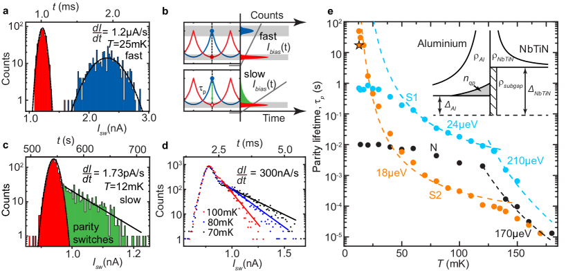
We model the CPT as a two level system which can exist in either parity state (red and blue bands in Fig. 1, respectively), and switches state on the timescale of \citeMPhysRevB.74.064515 due to quasiparticle tunneling. We collect the switching current histograms by repetitively sweeping the bias current from zero (non-dissipative state) to beyond the switching current. Here, in the resistive state, quasiparticle tunneling causes a random reinitialization of the parity state of the CPT for the next measurement. This results in the apparent 1e periodicity in Fig. 1c. Nevertheless, as long as the parity remains constant during each sweep, we expect to find the two branches as a bimodal histogram, as we indeed observe in Fig. 2a. In these measurements, the current ramp time is much shorter than the parity lifetime, (fast measurement limit).
We quantify in the slow measurement limit. In this regime parity switches occur during the current ramp (Fig. 2b lower panels) such that reaching the upper branch (depicted as blue in Fig. 2a and 2b) becomes exponentially suppressed (Fig. 2c). The exponential tail represents parity switches during the current bias ramp, resulting in an observable decay of the upper branch (depicted as green in Fig. 2b and 2c), . Thus, from the decay of the histogram (black solid line in Fig. 2c), we can directly obtain .
The observed is a result of single electron tunneling events through the junctions of the CPT. In the zero voltage state, we can link to the subgap density of states on the island and the quasiparticle density in the leads \citeMPhysRevB.85.012504 (for details see the supplementary material):
| (1) |
where is the normal state resistance of the CPT. It is instructive to note that the parity lifetime is determined by the quasiparticle density in the leads \citeMPhysRevB.85.174533 and the phenomenological Dynes parameter \citeMPhysRevLett.41.1509 of the island material. Assuming a thermal in the leads, we find eV (Fig. 2e) for temperatures exceeding mK, in good agreement with the superconducting gap of the aluminium leads extracted from the charge stability diagram. We can therefore attribute the observed parity lifetime for mK to the thermal quasiparticle population in the leads.
For device N, however, we find a saturated ms in the low temperature limit, a common observation in superconducting qubits \citeMRiste2013 and hybrid single electron transistors \citeMPhysRevB.85.012504 signifying the presence of non-thermal quasiparticle excitations.
We further improve the low temperature parity lifetime by introducing microwave-tight shielding coated with infrared absorber painting and Ti/Au quasiparticle traps for devices S1 and S2. These additions result in a non-saturated behaviour of , and we observe a minigap activated behaviour with eV for both devices. It is to be stressed that this observation signals that the effective quasiparticle temperature of the CPT follows the bath temperature down to the mK regime. We find s at mK for device S2. To put this number into context, we note that the Josephson frequency GHz and thus a single quasiparticle event occurs only once for every Cooper pairs tunneling through the junctions. This signifies the low probability of parity switches for an open device with required for flux-tunable Majorana braiding schemes.
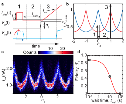
Thus far, we started each switching current measurement from an unknown parity state because of the random reinitialization in the dissipative state of the CPT for . In order to reproducibly select the same parity state, we employ a parity distillation protocol (Fig. 3) where, by selecting a single parity state without switching to the resistive state, we ensure that the parity remains well defined for the subsequent measurement. This protocol indeed results in a 2e periodic switching current pattern (Fig. 3c) which is observed for the first time for a non-aluminium CPT.
We quantify the effectiveness of the parity distillation by defining the fidelity as:
| (2) |
where is the conditional probability of the upper branch in the final step (3), and is the initial probability. We note that the above expression is valid for an arbitrary value set by the average quasiparticle occupation of the CPT. For device S2 we find for ms demonstrating the high degree of parity distillation. By changing between the parity initialization (1) and measurement (3), we acquire an independent measurement s for device S2 at mK (Fig. 3d).
Finally, we investigate the evolution of in different magnetic field directions. In parallel magnetic field, we observe a gradual decrease of . The onset of the steep decay at mT (yellow arrow in Fig. 4a) is in agreement with the condition for vortex penetration through a mesoscopic superconducting island \citeMMoshchalkov1995 with . This result underlines the significance of the sample geometry for magnetic field-enabled CPTs to avoid vortex formation. However, our device exhibits ms in mT, required to induce Majorana bound states \citeMPhysRevLett.105.077001, PhysRevLett.105.177002, Mourik25052012.
In contrast, applying a perpendicular field first results in an increase of reaching a maximum value s at mT, before dropping at higher magnetic fields (Fig. 4b). Making use of the relation between the lower critical field and the stripe width, \citeMPhysRevLett.92.097003 we attribute the initial increase to vortex formation and hence more effective quasiparticle trapping in the wide lead sections (m) of the device (see wide light gray sections in Fig. 4b). Upon reaching mT, the vortex phase becomes stable in the close vicinity of the CPT (nm) causing a gradual decrease of . We note that due to for our devices, we cannot make a quantitative comparison between our measurement data and theoretical expressions of critical magnetic field of thin stripes. We however conclude that vortices induced by a perpendicular magnetic field can increase the efficiency of quasiparticle traps, but the formation of a vortex phase in the near vicinity of the CPT enhances quasiparticle transport in agreement with earlier observations \citeMPhysRevB.84.220502, wang2014.
In conclusion, we fabricated and characterized NbTiN Cooper-pair transistors showing parity effects for a non-aluminium superconductor for the first time. We characterize the parity lifetime by evaluating the switching current histograms and find values exceeding 1 minute at mK. Our devices are in the regime of ideal for Majorana braiding schemes. Furthermore, we demonstrate charge parity distillation to reproducibly initialize the island in a given parity state. We find parity lifetimes in excess of ms in external magnetic fields up to mT and showed the importance of sample geometry for magnetic field-enabled operation required for inducing Majorana bound states.
The authors thank A. R. Akhmerov, S. Rubbert, Y. Nazarov, R. Lutchyn and J. Pekola for fruitful discussions and R. N. Schouten for technical assistance. This work has been supported by the Netherlands Foundation for Fundamental Research on Matter (FOM) and Microsoft Corporation Station Q. A. G. acknowledges funding from the Netherlands Organisation for Scientific Research (NWO) through a VENI grant.
D. J. W. fabricated the devices. D. J. W. and A. G. performed the measurements. D. J. W., A. G. and L. P. K. discussed the data, contributed to the analysis and wrote the manuscript.
references
Supplementary online material
1 minute parity lifetime of a NbTiN Cooper-pair box
I Device fabrication
The Cooper-pair transistors (CPTs) were fabricated using electron beam lithography and thin film deposition starting with a p++ doped silicon wafer with a nm thick thermally grown SiO2 surface layer. First, aluminium leads were defined and evaporated in a high-vacuum chamber (Torr) at a rate of nm/s with a thickness of nm. Subsequently, the mask for the NbTiN island was defined in a second lithography step. The sample was loaded into an ultra high vacuum AJA International ATC 1800 sputtering system (Torr), where first a nm Al layer was removed by means of argon plasma etching at mTorr. This step was followed by in-situ oxidization to create AlOx tunnel barriers. Without breaking vacuum, the NbTiN island was then sputtered with a layer thickness of nm.
We used a Nb0.7Ti0.3 target with a diameter of . Reactive sputtering resulting in nitridized NbTiN films was performed in an Ar/N process gas with a typical nitrogen content at a pressure of mTorr using a DC magnetron source. During deposition, a V bias was applied to the sample with respect to the target. The critical temperature of the superconducting transition temperature of thin films with a layer thickness of nm was measured to be K in zero magnetic field.
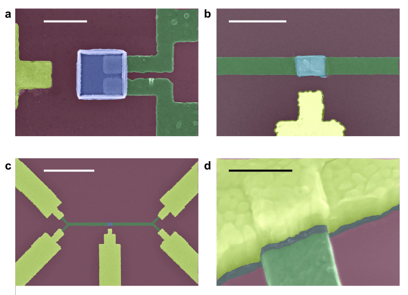
For the shielded samples S1 and S2, quasiparticle traps were fabricated by first cleaning the Al surface by means of argon plasma milling at mTorr and in-situ evaporation of nm Ti and nm Au films at a base pressure of Torr (see Fig. S1c and d).
Care was taken to remove resist mask residues after each electron beam writing step using a remote oxygen plasma etch with a pressure of mbar.
| device | island size | junction size | NbTiN thickness | traps | oxygen exposure | |
|---|---|---|---|---|---|---|
| (nmnm) | (nmnm) | (nm) | (Torrs) | (k) | ||
| N | 70 | no | 7400 | 58 | ||
| S1 | 100 | yes | 150 | 125 | ||
| S2 | 100 | yes | 150 | 66 |
II Measurement setup
The measurements were performed in a Leiden Cryogenics CF-1200 dry dilution refrigerator with a base temperature of mK equipped with Cu/Ni shielded twisted pair cables thermally anchored at all stages of the refrigerator.
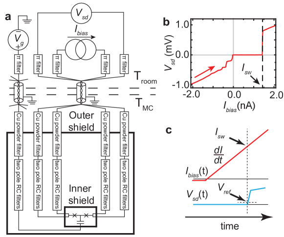
Fig. S2a shows the schematics of the measurement. The current bias and gate voltage were applied through battery operated and optically isolated sources in order to reduce line interference. Similarly, the first stage of the amplifier was isolated from the commercial readout electronics. Filtering of the measurement lines was achieved by room temperature LC filters with a cutoff frequency of MHz followed by a sequence of a high frequency copper powder filter \citeSs:/content/aip/journal/rsi/84/4/10.1063/1.4802875 and a two-pole RC filter with a nominal kHz, both thermally anchored to the mK stage.
Special care was taken to avoid stray microwave radiation by using an outer and an inner copper shield enclosing the device. The inner surface of both shields was treated with commercially available Aeroglaze Z306 paint \citeSsaeroglaze absorbing far infrared stray radiation \citeSs:/content/aip/journal/rsi/70/5/10.1063/1.1149739. We note that the inner shield was not present for device N.
A typical DC trace of device S2 at mK temperature is presented in Fig. S2b exhibiting a sharp transition between the dissipationless and the resistive state at the switching current, . We observe a retrapping current characteristic to unshunted Josephson junctions in the low temperature limit \citeSsMassarotti2012. The additional features in the resistive state are consistent with Fiske steps \citeSsPhysRev.138.A744.
The switching current histograms were acquired using a Rigol DG4062 arbitrary waveform generator controlling the isolated current bias source with a triangle wave signal resulting in a current ramp. A finite voltage response above the preset V triggers the recording of (Fig. S2c). We note that the delay of the low pass filters were accounted for on the basis of circuit simulations. Subsequent measurements were taken with setting zero for approximately ms in between to avoid overheating effects. We did not observe a difference in the switching current histograms taken with waiting times in the range of ms and s.
III Basic characterization of the CPT
In Fig. S3a we present a typical charge stability diagram of the CPT. First, we establish the superconducting gap of the aluminium lead and NbTiN island by finding the onset of quasiparticle transport (Fig. S3b and c).

| device | |||||||
|---|---|---|---|---|---|---|---|
| (eV) | (eV) | (k) | (eV) | (eV) | calc. | ||
| N | 210 | 1390 | 58 | 54 | 50 | 1.08 | 1.25 |
| S1 | 218 | 1420 | 125 | 21 | 62 | 0.34 | 0.32 |
| S2 | 220 | 1300 | 66 | 48 | 49 | 0.98 | 1.16 |
It is important to note that we find a finite subgap conductance at which is consistent with the presence of the subgap quasiparticle states justifying the analysis leading to equation (1) in the main text. Furthermore, we observe reduced meV values compared to that of bulk films (meV) \citeSs1212327, which we attribute to the chemical interaction between the AlOx tunnel barrier and the NbTiN film. Indeed, it was shown earlier that the critical temperature of Nb films is particularly very sensitive to contamination with oxygen \citeSsPhysRevB.9.888, sHalbritter1987. However, the nitridized NbTiN compound is presumably less prone to oxidization \citeSsDarlinski1987.
We evaluate the Josephson coupling for a single tunnel junction \citeSsPhysRevLett.10.486:
| (S1) |
with being the complete elliptic integral of the first kind. This expression is valid in the zero temperature limit, assuming symmetric tunnel junctions of the resistance of .
We estimate the charging energy, , based on the periodicity of characteristic resonances visible for (Fig. S3a) \citeSsPhysRevLett.73.1541, sPhysRevB.76.172505.
Alternatively, we can estimate the ratio based on the modulation of as a function of the gate charge, (last column of Table S2) \citeSsPhysRevLett.70.2940. We find a good agreement between the values acquired by the two independent methods.
IV Evaluation of the parity lifetime
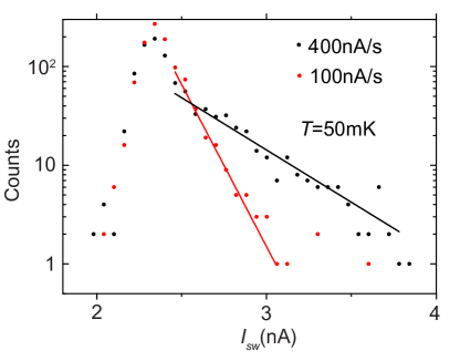
We checked the robustness of the extracted parity lifetime against changing the current ramp rate. Typical datasets are shown in Fig. S4, giving ms and ms for nA/s (red) and nA/s (black), respectively. We estimate the typical uncertainty to be , concluding that does not depend on which validates the analysis in the main text. However, we do not discuss here the intrinsic peak shapes of the bimodal switching current histogram. Since fast gate charge noise influences the measured distribution \citeSsjoyezthesis, we cannot distinguish between thermally activated \citeSsPhysRevB.9.4760 and macroscopic quantum tunneling behaviour \citeSsClarke2008, sMassarotti2012.
We now turn to the temperature dependence of . In order to get equation (1) in the main text, we assume the following:
-
i)
The superconducting gap of the island (meV) is much higher than the effective thermal energy describing the quasiparticle population and the gap of the leads (eV).
-
ii)
The density of states in the leads is BCS-type: for and zero otherwise.
-
iii)
There is a constant, finite subgap density of states for energies below in the island.
-
iv)
the energy dependence of the single electron tunnel probability is negligible over the energy range of , meaning that the tunnel barrier is much higher than .
-
v)
The tunnel barriers are identical, each characterized by half the normal state resistance of the full device, .
Considering only single electron tunneling and zero voltage bias across the tunnel barriers, following \citeSsPhysRevB.85.012504, we get the quasiparticle tunnel rate:
| (S2) |
Assigning an effective temperature to the quasiparticle population in the leads, we find:
| (S3) |
in the limit of . For temperatures exceeding mK, we assume that the quasiparticle population is in thermal equilibrium, and therefore the lattice temperature is equivalent to the effective quasiparticle temperature:
We verify this picture by fitting the observed parity lifetimes with as a free parameter, and find values ranging eV for different devices in good correspondence with the gap determined by voltage bias spectroscopy ( in Table S2).
Notably, the ratio is the Dynes parameter \citeSsPhysRevLett.41.1509 of the island material, characterized to be based on measurements of highly resistive single junctions. With this value and using \citeSsPhysRevB.85.012504, we get for device N based on the observed parity lifetime of ms in the low temperature limit.
We now comment on the observed eV activation energy observed for devices S1 and S2. We estimate the maximal even-odd energy difference to be eV based on eV \citeSsPhysRevB.75.212501 which is in range of the experimentally observed . Similar, activated behaviour of the parity lifetime scaling as was reported earlier \citeSsPhysRevB.77.100501.
Providing another possible explanation, we note that a grain size of nm can lead to a level spacing of the order of eV which can influence single electron transport and hence if the grains are weakly coupled, i. e. for disordered superconducting films \citeSsdubi2007. Disorder-induced fluctuations may also explain the broadening of the coherence peaks (Fig. S3c) \citeSssacepe2011, sPhysRevB.88.180505.
V Superconducting thin film characterization and magnetic field dependence
Next, we consider the properties of superconducting stripes with layer thickness , and a width to find the London penetration depth and the coherence length . We characterize the upper critical field in the parallel () and perpendicular geometry () based on the traces of the tunnel junctions of the CPT. In addition, we measure the normal state resistivity of the films that gives an estimate for the mean free path, \citeSskittelbook.
First, we establish the length scales of the island material, NbTiN. We find films superconducting at T which leads to an upper limit of nm following \citeSstinkhambook:
| (S4) |
The penetration depth can be estimated using the normal state resistivity of cm and the critical temperature of K using the following semi-empirical formula \citeSs1212327:
| (S5) |
Next we estimate length scales of the Al leads based on the electronic transport through the CPT. Typical thin Al films are type-II superconductors in the dirty limit () with a reduced coherence length of and with a London penetration depth of , where nm and nm are the bulk values \citeSstinkhambook. For our films, we estimate nm based on the resistivity of cm \citeSskittelbook. From the stability diagram of the devices, we extract upper critical fields of mT (Fig. S5d) and mT (Fig. S5b) leading to a coherence length of nm and nm which enables vortex formation in the aluminium leads in perpendicular magnetic field.
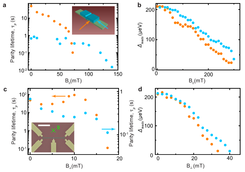
It is important to observe that nm enables vortex formation for an in-plane geometry in the NbTiN island. We find a characteristic suppression of at mT for device S2 (orange dots in Fig. S5a) and at mT for device S1 (cyan dots in Fig. S5a). Considering the effective cross-sectional areas (see Table S1 for dimensions), we find and for S2 and S1, respectively, which is in qualitative agreement with the threshold of a single vortex formation in a mesoscopic island \citeSsMoshchalkov1995, sGeim1997, sPhysRevB.58.R5948. We also note that of the leads (Fig. S5b) does not depend on the direction of , therefore the different evolution of can only be explained by the different alignment of with respect to the NbTiN islands.
In a perpendicular geometry, the vortex phase is stable in a thin stripe above the magnetic field
| (S6) |
where is a model-dependent prefactor \citeSsPhysRevLett.92.097003, sPhysRevB.84.220502, sPhysRevB.51.3092 of the order of unity. We reproducibly find the same non-monotonic behaviour of for devices S1 and S2 with the maximum at mT, which is in range of for nm, the width of the Al leads near the island.
references_supplement