Thermal Creation of Electron Spin Polarization in n-Type Silicon
Abstract
Conversion of heat into a spin-current in electron doped silicon can offer a promising path for spin-caloritronics. Here we create an electron spin polarization in the conduction band of n-type silicon by producing a temperature gradient across a ferromagnetic tunnel contact. The substrate heating experiments induce a large spin signal of , corresponding to spin-splitting in the conduction band of n-type silicon by Seebeck spin tunneling mechanism. The thermal origin of the spin injection has been confirmed by the quadratic scaling of the spin signal with the Joule heating current and linear dependence with the heating power.
Ultra large scale integration and miniaturization of electronic devices and circuitry yield to an increase in Joule heat dissipation and wastage of energy. An effort to reduce, reuse or redirect this heat is not only of technological, but also has fundamental and ecological importance. In this regard caloritronics explores the possibility of directly converting heat into electricity Snyder and Toberer (2008). On the other hand spintronics offers a promising path to achieve lower energy consumption Žutić et al. (2004); Fert (2008). An exciting new research field taking advantage of both of these areas, called spin-caloritronics, is attracting a growing interest Bauer et al. (2012); Johnson and Silsbee (1987). Recently, many physical phenomena connecting spin to thermal effects have been proposed and demonstrated such as spin-Seebeck effect Uchida et al. (2008), spin dependent Seebeck effect in nanostructures and thermal spin injection into metal Slachter et al. (2010), thermal spin-transfer torque Hatami et al. (2007); Yu et al. (2010), spin-related Peltier cooling Flipse et al. (2012), and thermal spin tunnel effects Walter et al. (2011); Le Breton et al. (2011). Especially interesting is the Seebeck spin tunneling into semiconductors, which is sensitive to the energy derivative of tunnel spin polarization at the interfaces Le Breton et al. (2011).
The strong interest in Si for spintronics stems from its long spin coherence length, caused by the absence of hyperfine interactions and a weak spin-orbit coupling, and its industrial dominance Jansen (2012); Jansen et al. (2012a). Recently, electrical spin polarization in Si could be created at room temperature by spin polarized tunneling from a ferromagnet (FM) Dash et al. (2009); Jansen et al. (2010); Sasaki et al. (2009); Jeon et al. (2011); Li et al. (2011). The Hanle and the inverse of the Hanle effects were used for the detection of spin polarization in different semiconductors under ferromagnetic tunnel contacts Dash et al. (2011). Using such Hanle techniques, Le Breton et al. demonstrated a spin accumulation in hole doped p-type Si by using the Seebeck spin tunneling mechanism Le Breton et al. (2011). In a FM/tunnel barrier/semiconductor structure, a temperature difference between the electrodes creates a tunnel spin current Le Breton et al. (2011); Jansen et al. (2012b); Jain et al. (2012); Jeon et al. (2012), which is governed by the energy derivative of the tunnel spin polarization (TSP). This involves thermal transfer of spin angular momentum from the ferromagnet to Si without net tunneling charge current. For Si based devices, these experiments are yet limited to reports on hole doped p-type Si with Al2O3 / NiFe tunnel contacts Le Breton et al. (2011). For further development, it is required to have spin tunnel contacts with strong variation in TSP around the Fermi energy (EF), tunnel barriers with high interface thermal resistances, and its implementation in both electron and hole doped Si Le Breton et al. (2011). Therefore, a detailed investigation of spin Seebeck tunneling effect with new ferromagnetic tunnel contact materials, and electron doped n-type Si is crucial from fundamental and technological point of view.
In this letter, we report a thermal creation of electron spin polarization in n-type Si by using the Seebeck spin tunneling mechanism. The temperature gradient between the n-type Si substrate and the FM yields to Seebeck spin tunnel currents, creating a large spin accumulation in the Si conduction band. We particularly use ferromagnetic tunnel contacts with ozone oxidized SiO2 tunnel barriers and Co ferromagnet on heavily doped n-type Si. The detection of this thermally induced spin polarization was performed by employing Hanle and inverted Hanle effects in four-terminal measurement geometry. The amplitude of the thermal spin signal scales quadratically with the Joule heating current density and linearly with the heating power, which confirms the thermal origin of the observed Hanle signal. Electrical measurements and high magnetic field experiments rule out any other type of thermomagnetic effects. This result offers a way to generate a large electron spin accumulation in n-type Si by thermal spin injection using Seebeck spin tunneling.
For thermal spin injection into the n-type Si (measured electron density of at ) FM tunnel contacts (Co/SiO2) were fabricated on initially patterned thick silicon-on-insulator (SOI) channels (with the dimensions ). The SiO2 tunnel barrier was formed on the Si by ozone oxidation at room temperature. The chips were exposed to O3, created by a constant O2 flow () in the presence of a UV radiation source. This process results in uniform and pinhole-free tunnel barriers of thickness. This is confirmed by the temperature and thickness dependent measurements of the junction resistance Dankert et al. (2013). Using such SiO2 tunnel barrier, a very large spin polarization in silicon could be achieved by electrical method Dankert et al. (2013). After oxidation the samples were transferred to an electron beam deposition system, where Co and 10 nm Au were deposited. The FM contacts were patterned by photolithography and Ar–ion beam etching. Subsequently, Cr ()/Au () contacts on the Si, and contact pads on the ferromagnetic tunnel contacts were prepared by photolithography and lift-off technique. The Cr/Au contacts were used for the Joule heating of the Si and as reference contacts to detect a voltage signal with respect to the FM tunnel contact. The ferromagnetic tunnel contacts have an area of allowing a sufficiently good signal-to-noise ratio.
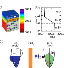
The principle for the thermal creation of spin accumulation in Si using the Seebeck spin tunneling mechanism is illustrated in Fig. 1. The simulated temperature distribution across the interface of the Co/SiO2 ()/n-type Si device is shown in Fig. 1a and b. The complete device structure of Au ()/Co ()/SiO2 ()/n-type Si () were considered for our calculation. A model was drawn to scale with our device and divided into finite elements using commercial software (COMSOL) for calculating their temperatures. The temperature gradient () is created by dissipation of an applied current density of . The simulation takes Joule heating due to current flow and heat dissipation, transport and radiation into account with a base temperature of . Here we have used a heat conductance for thin SiO2 tunnel barriers Yamane et al. (2002). Taking the large thermal conductivity of the Au pads and wire bonding into account, the surface temperature of the contact pads was fixed to . This results in a temperature gradient between the Si () and Co (). Such temperature difference yields to a nonequilibrium electron distributions in the Co and Si near the Fermi energy. This results in tunneling of equal number of electrons in opposite directions, giving rise to a zero net charge current. However, as the energy dependence of is known to be different for the forward and reverse tunneling processes Valenzuela et al. (2005); Park et al. (2007), a spin accumulation () can be induced in the Si (Fig. 1c) Le Breton et al. (2011); Jansen et al. (2012b).
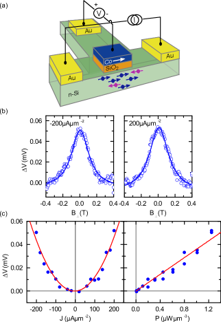
Before performing thermal spin injection experiments we have tested the contacts for electrical spin injection and verified the energy or bias dependence of . The measurements were performed in a three-terminal Hanle geometry as shown in Fig. 2a. Electrical spin injection creates a majority spin accumulation and splitting of the electrochemical potential in the conduction band of the Si. The Hanle effect is used for the controlled reduction of the induced spin accumulation by applying a magnetic field () perpendicular to the FM magnetization direction. The spin accumulation decays as a function of with an approximately Lorentzian line shape given by , where and are the spin accumulations in zero and finite perpendicular magnetic field, respectively, and is the lower limit for spin lifetime Dash et al. (2009); Dankert et al. (2013). Figure 2b shows the measurement of the electrical Hanle signal for bias currents of (corresponding bias voltage of ) at . The spin injection () from the Co/SiO2 tunnel contact creates a majority spin () accumulation, whereas the spin extraction () creates a minority spin () accumulation in the Si. As expected the measured Hanle signal for majority and minority spin accumulation are found to be of opposite sign. The spin accumulation scales with the tunnel spin polarization () of the injected current and with spin life time (). The detected voltage due to spin accumulation can be written as . This results in the detected spin signal (spin resistance area product, spin-RA) which is proportional to . The variation of vs. bias voltage is presented in Fig 2d and is found to be asymmetric. The strong decay of for energies above () results in the direction dependent spin polarized tunnel currents Le Breton et al. (2011); Jansen et al. (2012b). The difference in spin polarization of the currents tunneling into and out of the Si can yield to a spin injection in our Co/SiO2/n-type Si devices Le Breton et al. (2011); Valenzuela et al. (2005); Park et al. (2007). This asymmetry in the of Co/SiO2/n-type Si contact is essential to induce the large thermal spin accumulation in Si via Seebeck spin tunneling mechanism.
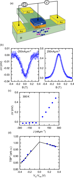
The thermally induced electron spin accumulation in n-type Si has been created by introducing a temperature gradient between the Si () and Co () separated by a thin SiO2 tunnel barrier (). We increase the temperature of Si channel () by a DC current due to Joule heating. The SiO2 tunnel barrier prevents the current and heat from spreading into the ferromagnetic electrode. The temperature gradient created across the SiO2 barrier () results in spin polarized Seebeck tunnelling through the oxide barrier, since the for ingoing and outgoing currents differs. This creates a spin accumulation in the Si conduction band and therefore a splitting of the electrochemical potential () as shown in Fig 1c. The detection of a thermally induced spin accumulation in Si is performed in both Hanle and inverted Hanle geometry using a SiO2/Co contact Le Breton et al. (2011); Dash et al. (2009). A voltage signal is detected while sweeping a magnetic field, under the condition of zero net tunnel charge current () between the Co and the Si Le Breton et al. (2011); Dash et al. (2009).
A significant thermal Hanle spin accumulation signal of is observed in the Si for , for a Joule heating current density of (Fig. 3b). The Lorenzian line shape of the thermal Hanle signal obtained here is consistent with our electrical Hanle measurements. The magnitude and sign of the thermal Hanle curves are also identical for both directions of the Joule heating current. This is expected, since the Joule heating and therefore the gradient should be independent of current direction. For a spin polarization identical to the electrical spin injection is observed, which corresponds to majority spin accumulation in the Si. This should be the case for a decaying above as confirmed by our electrical bias dependence measurements presented in Fig. 2d. Figure 3c shows the amplitude of the thermal Hanle signal measured for different Joule heating currents. The amplitude of the thermal spin signal is found to scale quadratically with the heating current density and hence linearly with the applied heating power, which confirms the thermal origin of the Hanle signal Le Breton et al. (2011).
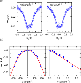
Furthermore, we employ the inverted Hanle effect Dash et al. (2011) to detect the thermal creation of spin accumulations in Si at room temperature. The local magnetostatic fields arising from interface roughness in a ferromagnetic tunnel contact is known to reduce the spin accumulation in semiconductors. The inverted Hanle effect serves as experimental signature which recovers the reduced spin accumulation by applying an in-plane magnetic field Dash et al. (2011). Figure 4 shows the measured data due to thermal spin injection for the case of in the same Co/SiO2/n-type Si device. An inverted thermal Hanle signal of could be detected for a current density of (Fig. 4a). As the Joule heating is independent of the current direction, spin signals of same sign and magnitude are obtained for both current directions. Figure 4b shows the amplitude of the inverted thermal Hanle signal for different Joule heating currents, which is also found to scale quadratically with the heating current density and linearly with the applied heating power. This scaling of the spin signal is consistent with a thermally induced spin accumulation in Si Le Breton et al. (2011).
The total magnitude of the thermal spin accumulation in n-type Si is the sum of the Hanle () and inverted Hanle () amplitudes Dash et al. (2011). A total thermal spin signal of corresponds to a spin splitting (, assumed for SiO2/Co contact). This corresponds to an electron spin polarization of 1% in the n-type Si conduction band created by thermal spin injection at room temperature, considering a parabolic conduction band and a Fermi–Dirac distributions for each spin direction ( and ). The magnitude of the thermal spin accumulation defined in terms of a Seebeck spin tunneling coefficient , is found to be . There can be some discrepancy with theory due to inaccuracy in the determination of , as experimental values for the thermal conductance of different materials and their interfaces are unknown. For the cases of thin tunnel barriers, the interface thermal resistance dominates over the bulk values and also differs with sample preparation conditions. In addition, the ballistic phonon transport and confinement effects in ultra-thin dielectrics and interface roughness play an important role in altering the thermal resistance of the contacts Yamane et al. (2002).
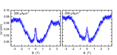
The linear dependence of the spin signal on the heating power confirms the thermal origin of spin accumulation in n-type Si. Furthermore, we can rule out other thermomagnetic effects such as spin related Hall, Nernst, and Ettingshausen effect, because they would not produce the characteristic Lorentzian shape Hanle signal Le Breton et al. (2011). Nevertheless, to rule out all known thermomagnetic effects, measurements at high magnetic fields were performed. For large enough the magnetization of the FM rotates out of the plane. This aligns the injected spins parallel to the magnetization direction and produces zero precession, resulting in a recovery of the dephased spin signal. This recovery of the spin signal occurs only if the spin accumulation is produced by a transfer of the spins from the FM. The experimental data for the spin accumulation induced by heating of the Si electrode for are shown in Fig. 5. Indeed, the recovery of the spin accumulation is observed when the magnetic field increases above , with the signal saturating at about . This corresponds to the field at which the magnetization of the Co electrode has reached the full out-of-plane orientation Sharma et al. (2012, 2014). The observation of the high-field recovery of the spin accumulation rules out the spin-Nernst effect and any other mechanism that does not involve transfer of spins from the FM to the Si Le Breton et al. (2011).
In summary, we demonstrate the thermal creation of electron spin polarization in n-type Si using the Seebeck spin tunneling mechanism at room temperature. We show that the magnitude of thermally created electron spin polarization scales quadratic with the Joule heating current density and linearly with the heating power. A temperature gradient of few hundred milli kelvins across the ferromagnetic tunnel contacts creates a spin signal of more than , which corresponds to a spin splitting of and spin polarization of 1% in the conduction band of n-type Si. Furthermore, the control experiment with thermal Hanle measurements at higher magnetic field and the comparison with electrical spin injection experiments rules out any other spurious effects. The advantage of utilizing the Seebeck spin tunneling mechanism is that the magnitude of spin accumulation is not limited to the of ferromagnetic tunnel contact, but can be increased beyond that due to its dependence on energy derivative of . Recently, similar results using MgO tunnel barrier have been reported, during review process of our manuscript Jeon et al. (2013). By carefully designing the interfaces, Seebeck spin tunneling could be useful for creating spin polarizations in non-magnetic materials by itself or together with electrical spin injection, and also for the reusing dissipated heat in electronic devices and circuits.
Acknowledgement: The authors acknowledge the support of colleagues at the Quantum Device Physics Laboratory and Nanofabrication Laboratory at Chalmers University of Technology. We would also like to acknowledge the financial supported from the Nano Area of the Advance program at Chalmers University of Technology, EU FP7 Marie Curie Career Integration grant and the Swedish Research Council (VR) Young Researchers Grant.
References
- Snyder and Toberer (2008) G. J. Snyder and E. S. Toberer, Nat. Mater. 7, 105 (2008).
- Žutić et al. (2004) I. Žutić, S. Das Sarma, J. Fabian, and S. D. Sarma, Rev. Mod. Phys. 76, 323 (2004).
- Fert (2008) A. Fert, Rev. Mod. Phys. 80, 1517 (2008).
- Bauer et al. (2012) G. E. W. Bauer, E. Saitoh, and B. J. van Wees, Nat. Mater. 11, 391 (2012).
- Johnson and Silsbee (1987) M. Johnson and R. Silsbee, Phys. Rev. B. 35, 4959 (1987).
- Uchida et al. (2008) K. Uchida, S. Takahashi, K. Harii, J. Ieda, W. Koshibae, K. Ando, S. Maekawa, and E. Saitoh, Nature 455, 778 (2008).
- Slachter et al. (2010) a. Slachter, F. L. Bakker, J.-P. Adam, and B. J. van Wees, Nat. Phys. 6, 879 (2010).
- Hatami et al. (2007) M. Hatami, G. Bauer, Q. Zhang, and P. Kelly, Phys. Rev. Lett. 99, 066603 (2007).
- Yu et al. (2010) H. Yu, S. Granville, D. P. Yu, and J.-P. Ansermet, Phys. Rev. Lett. 104, 146601 (2010).
- Flipse et al. (2012) J. Flipse, F. L. Bakker, a. Slachter, F. K. Dejene, and B. J. van Wees, Nat. Nanotechnol. 7, 166 (2012).
- Walter et al. (2011) M. Walter, J. Walowski, V. Zbarsky, M. Münzenberg, M. Schäfers, D. Ebke, G. Reiss, A. Thomas, P. Peretzki, M. Seibt, J. S. Moodera, M. Czerner, M. Bachmann, and C. Heiliger, Nat. Mater. 10, 742 (2011).
- Le Breton et al. (2011) J.-C. Le Breton, S. Sharma, H. Saito, S. Yuasa, and R. Jansen, Nature 475, 82 (2011).
- Jansen (2012) R. Jansen, Nat. Mater. 11, 400 (2012).
- Jansen et al. (2012a) R. Jansen, S. P. Dash, S. Sharma, and B. C. Min, Semicond. Sci. Technol. 27, 083001 (2012a).
- Dash et al. (2009) S. P. Dash, S. Sharma, R. S. Patel, M. P. de Jong, and R. Jansen, Nature 462, 491 (2009).
- Jansen et al. (2010) R. Jansen, B. C. Min, S. P. Dash, S. Sharma, G. Kioseoglou, A. T. Hanbicki, O. M. J. van ’t Erve, P. E. Thompson, and B. T. Jonker, Phys. Rev. B 82, 241305 (2010).
- Sasaki et al. (2009) T. Sasaki, T. Oikawa, T. Suzuki, M. Shiraishi, Y. Suzuki, and K. Tagami, Appl. Phys. Express 2, 053003 (2009).
- Jeon et al. (2011) K. Jeon, B. Min, I. Shin, C.-Y. Park, H.-S. Lee, Y. Jo, and S. Shin, Appl. Phys. Lett. 98, 262102 (2011).
- Li et al. (2011) C. H. Li, O. M. J. van ’t Erve, and B. T. Jonker, Nat. Commun. 2, 245 (2011).
- Dash et al. (2011) S. P. Dash, S. Sharma, J.-C. Le Breton, J. Peiro, H. Jaffrès, J.-M. George, A. Lemaître, and R. Jansen, Phys. Rev. B 84, 054410 (2011).
- Jansen et al. (2012b) R. Jansen, A. M. Deac, H. Saito, and S. Yuasa, Phys. Rev. B 85, 1 (2012b).
- Jain et al. (2012) A. Jain, C. Vergnaud, J. Peiro, J. C. Le Breton, E. Prestat, L. Louahadj, C. Portemont, C. Ducruet, V. Baltz, A. Marty, A. Barski, P. Bayle-Guillemaud, L. Vila, J.-P. Attané, E. Augendre, H. Jaffrès, J.-M. George, and M. Jamet, Appl. Phys. Lett. 101, 022402 (2012).
- Jeon et al. (2012) K. Jeon, B. Min, Y. Park, and Y. Jo, Appl. Phys. Lett. (2012).
- Dankert et al. (2013) A. Dankert, R. S. Dulal, and S. P. Dash, Sci. Rep. 3, 3196 (2013).
- Yamane et al. (2002) T. Yamane, N. Nagai, S.-i. Katayama, and M. Todoki, J. Appl. Phys. 91, 9772 (2002).
- Valenzuela et al. (2005) S. Valenzuela, D. J. Monsma, C. Marcus, V. Narayanamurti, and M. Tinkham, Phys. Rev. Lett. 94, 196601 (2005).
- Park et al. (2007) B. G. Park, T. Banerjee, J. Lodder, and R. Jansen, Phys. Rev. Lett. 99, 23 (2007).
- Sharma et al. (2012) S. Sharma, S. P. Dash, H. Saito, S. Yuasa, B. J. van Wees, and R. Jansen, Phys. Rev. B 86, 165308 (2012).
- Sharma et al. (2014) S. Sharma, A. Spiesser, S. Dash, S. Iba, S.Watanabe, B. J. van Wees, H. Saito, S. Yuasa, and R. Jansen, Phys. Rev. B 89, 075301 (2014).
- Jeon et al. (2013) K.-R. Jeon, B.-C. Min, S.-Y. Park, K.-D. Lee, H.-S. Song, Y.-H. Park, and S.-C. Shin, Appl. Phys. Lett. 103, 142401 (2013).