Tunable THz Surface Plasmon Polariton based on Topological Insulator-Layered Superconductor Hybrid Structure
Abstract
We theoretically investigate the surface plasmon polariton (SPP) at the interface between 3D strong topological insulator (TI) and layered superconductor-magnetic insulator structure. The tunability of SPP through electronic doping can be enhanced when the magnetic permeability of the layered structure becomes higher. When the interface is gapped by superconductivity or perpendicular magnetism, SPP dispersion is further distorted, accompanied by a shift of group velocity and penetration depth. Such a shift of SPP reaches maximum when the magnitude of Fermi level approaches the gap value, and may lead to observable effects. The tunable SPP at the interface between layered superconductor and magnetism materials in proximity to TI surface may provide new insight in the detection of Majorana Fermions.
pacs:
73.20.Mf, 73.25.+iI Introduction
Surface plasmon polariton (SPP) is the collective excitation of electrons at the interface between conductor and dielectrics driven by electromagnetic (EM) waves. Pitarke et al. (2007); Maier (2007) Despite its wide applications in nanophotonics Nanophotonics (2007), near- field optics and tip-enhanced Raman spectroscopy Kawata (2001); Cui et al. (2014), and biological sensors and antennas Homola (2006); Becker (2012), SPP in general suffers from problem of huge non-radiative loss due to the strong absorption of the metal Pitarke et al. (2007); Maier (2007); Nanophotonics (2007); Kawata (2001) accompanied with additional radiative loss Váry and Markoš (2010), which limits SPP’s lifetime and propagation length for further application in integrated devices.
In order to solve the SPP loss problem, the low-loss plasmonics based on graphene Wunsch et al. (2006); Hwang and Sarma (2007a); Jablan et al. (2009); Ju et al. (2011); Koppens et al. (2011); Yan et al. (2012a); Grigorenko et al. (2012); Maier (2012); Bao and Loh (2012); Tassin et al. (2012); Brar et al. (2013); Jin et al. (2013); Lu et al. (2013); Buljan et al. (2013); Avouris and Freitag (2014) and topological insulators (TI) Efimkin et al. (2012a, b); Roslyak et al. (2013); Schütky et al. (2013); Di Pietro et al. (2013); Okada and Madhavan (2013); Stauber et al. (2013); Chen et al. (2013) has attracted much recent attention. In far infrared and THz range, the major loss mechanism in graphene lies in the scattering between electrons and optical phonons Jablan et al. (2009). A number of studies in graphene plasmonics have been conducted utilizing the properties of low loss and tunability. Yan et al. Yan et al. (2012b) have reported enhanced plasmon resonance in patterned graphene-insulator stack structure comparing with single-layered graphene, while Ju et al Ju et al. (2011) demonstrated an enhanced tunability at THz range in micro-ribbon graphene metamaterials. These efforts target at manipulation of photons and miniaturization of optical devices, and could be further integrated and hybridized toward further applications in detectors, modulators or other integrated devices.
On the other hand, in doped 3D TI, the electron-impurity scattering becomes dominant due to weak electron-phonon coupling Di Pietro et al. (2013), with a further reduced backscattering probability thanks to topological protected surface states Bernevig (2013); Hasan and Kane (2010); Qi and Zhang (2011). However, unlike the booming studies in graphene plasmonics, the plasmon hybrid devices in TI have been seldom reported, even with comparable performance in THz range as well as additional features such as net spin polarization, i.e. “spin plasmon” Efimkin et al. (2012a, b); Roslyak et al. (2013); Chen et al. (2013) and spin-charge separation Stauber et al. (2013).
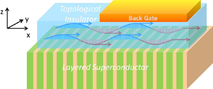
Therefore, in this paper, we propose a plasmonic hybrid structure composed of 3D TI in close contact with layered superconductor. This structure provides a new platform where SPP waves are supported. The tunability of the SPP propagation can be achieved independently through either gate voltage and magnetic field. Since the Majorana bound states, which are an non-Abelian anyons in superconductors and may have great impact in topological quantum computationHasan and Kane (2010), may exist at the boundary of 3D TI and superconductor, this plasmonic structure may provide a new perspective in search for Majorana bound states.
II Theory
II.1 Dispersion Relation of Anisotropic SPP Wave
Since the SPP wave is localized along the interface, and the Dirac electrons only exist on the surface of TI, we use anisotropic dielectric functions to model the dielectric function of a 3D TI in order to capture both the Dirac dielectric functions of 2D chiral Dirac electrons at the surface (Fig. 1, plane, ) as well as the dielectric constant in the bulk (Fig. 1, region).
In order to describe wave propagation in the layered structure( Fig. 1 region), we adopt the method proposed by Averkov et al Averkov et al. (2013) using anisotropic dielectric function. This is valid when , where is the SPP wavelength, and is the spatial periodicity of the layered structure. Since we are interested in long wavelength THz range, the condition that is guaranteed to meet.

In this approach, the anisotropy leads to the existence of optical axis where EM wave suffers no birefringence Hecht (1998). Thus the electric field and magnetic field at the interface can be written as a superposition of ordinary wave and extraordinary wave:
| (1) |
where is for the TI and layered superconductor side, respectively. Based on our model, the TI dielectric function is defined as with optical axis along direction, while the dielectric function of layered superconductor is defined as , which is anisotropic along direction.
By noticing the different direction of optical axis in the upper TI region and lower superconductor region, that for ordinary wave and extraordinary wave we have , , and , , respectively. The components of the EM fields are shown in Appendix A, with light speed in vacuum and is the magnetic permeability of the layered superconductor material.
Substituting the EM field components back to eq. (1), we obtain the localization constants, i.e. inverse of penetration depth away from the interface.
| (2) | |||||
| (3) | |||||
| (4) | |||||
| (5) |
The dispersion relation of the resulting surface wave can be written in a determinant form:
| (6) |
In this paper, we only consider the wave propagating along x direction, neglecting the oblique excitation. The dispersion relation can finally be simplified as
| (7) |
which is the main analytical result. In this expression, is the effective permeability of the layered superconductor structure, q is the wavenumber along direction, and can be a complex number. When both the upper and lower materials are isotropic, i.e. and , it is further reduced to the well-known result .
II.2 Dielectric Function of Layered Superconductor
Define dimensionless frequency , with the Josephson plasmon frequency of the layered superconductor, the dielectric function of layered superconductor can be written as Averkov et al. (2013):
| (8) |
where the imaginary parts are neglected. Throughout this article, we take the value reported in Averkov et al. (2013) and set the interlayer dielectric constant , current-anisotropy parameter and .
II.3 Dielectric Function of Gapless Topological Insulator
The dielectric function of the chiral gapless topological insulator surface have been reported in Efimkin et al. (2012a, b); Schütky et al. (2013), where for the Hamiltonian for 2D helical Dirac electron gas :
| (9) |
the Lindhard Dielectric function can be written as
| (10) |
with the polarization operator
| (11) |
In this expression, is the spin/valley degeneracy, for the chiral states we have due to spin-momentum locking, is Fermi occupation value at energy eigenvalue, , with for conduction band and for valence band, respectively. The spinor eigenstates , with defined as . We take the value of Fermi velocity Zhang et al. (2009) in all calculations.
Eq. (11) can be calculated either analytically Schütky et al. (2013); Hwang and Sarma (2007b)or numerically, thanks to the identical expression of polarization operator within RPA for simple Dirac gas and helical Dirac gas. In our approach, we choose for numerical integration to avoid discontinuity, and compare with analytical result with at least 6 digit agreement. Then the numerical result for gapless TI is applied to solve for the dielectric function of TI when surface state is gapped.
II.4 Dielectric Function of Gapped Topological Insulator
Either the magnetic field perpendicular to the interface (along direction in Fig. 1) or the superconductivity would open up a gap to the gapless Dirac cone, and lift out the degeneracy at , and further alter the dielectric function as well SPP dispersions. In order to take the effect of gaps into account, we adopt the Bogoliubov-de Gennes Hamiltonian Bernevig (2013); Fu and Kane (2008), which can be regarded as a generalization of eq. (8):
| (12) |
where spinor and denote the magnetic gap and superconductivity gap, respectively, is the chemical potential. Both eq. (10) and eq. (11) still hold, but the eigenvalues and eigenvectors are changed. The eigenvalues can now be written as
The corresponding unnormalized eigenvectors are shown in Appendix A.
When the surface state is gapped, the EM constitutive relations have been modified with an additional axion term Karch (2011) and leads to electromagnetic effect. However, it is shown that such effect Karch (2011); Li et al. (2013) only has correction to the SPP dispersion, where is the fine structure constant, thus in the present calculation we neglect the effect from axion electrodynamics
III Results and Discussions
In order to conveniently express the dielectric functions for both TI and layered superconductor, we define dimensionless wavenumber , and all energies are dimensionless and expressed in the unit of .


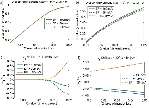
The SPP dispersion relations are obtained by solving Eq. (7). The typical dispersion relations at various gate voltages, i.e. Fermi levels , are shown in Fig. 2 a and b. We see an enhanced tunability, i.e. shift of dispersion relation when varies, when the lower layer has increased effective magnetic permeability . By defining the SPP group velocity , we see an additional change of propagation properties induced by either or (Fig. 2 c and d) by plotting the percentage SPP group velocity shift
Here both the magnetic gap and superconductivity gap are dimensionless in the unit of Josephson plasmon frequency .
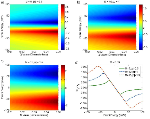
In order to further investigate the effect of gap to the SPP propagation, the relative shift of group velocity as a function of dimensionless wavenumber and Fermi level are shown in Fig. 3, at different values of gap. It can be seen directly that the shift is increased at larger gap value, and it increases as a function of Q. Most importantly, the shift reaches peak value when the Fermi level approaches to the gap value. This feature can be seen more clearly in a line plot with fixed value (Fig. 3 d).We also see that SPP group velocity does not shift when Fermi level .

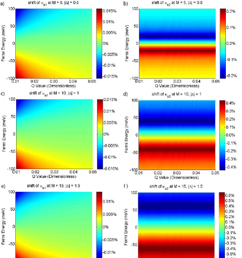
In contrary to the and dependent shift of group velocity caused by energy gap, the localization constants show a qualitatively different behavior. The localization constant in TI side is neither sensitive to nor to (Fig. 4 a, c, e), while in layered superconductor side, is tunable by but still -independent. The importance of the localization constant shift as can hardly be overestimated, in that it indicates that the different propagation properties of SPP is almost fully coming from the group velocity, other than the difference in SPP wavelength. The fewer controllable variables would indefinitely make the experimental results easier to explain.
The reason that the maximum shift occurs when the gap matches the Fermi level can be understood in the light of electronic transition and available electron density for plasmonic oscillation. Electrons in the conduction band are mostly extended and dominate the surface plasmon excitation. When the Fermi level is lower than the energy gap, charge carriers need additional energy to fulfill the transition to the conduction band in order to contribute to the collective excitation. On the other hand, since the SPP is excited by EM waves, when the Fermi level is higher than the energy gap, the electronic transition by optical excitation is limited by occupied electrons. The increasing forbidden transition leads to a reduced shift of dielectric function, and moreover the shift is reduced accordingly. Thus, only when the Fermi level reaches the value of energy gap are the number of available electrons participating in the electronic transition and collective excitation maximized, and leads to a shift of SPP frequency and group velocity.
IV CONCLUSIONS
We provide a generic theoretical framework to study the surface plasmon polariton (SPP) at the interface between topological insulator (TI) and layered superconductors. The SPP in this hybrid structure may be widely applied to study novel optical and transport phenomena at the interface, through the tunability of SPP propagation by gating or gapping the surface states of the TI. It can also be generalized to a larger category of materials in proximity to TI surface. For instance, Wei et al. Wei et al. (2013a, b) have shown that when the ferromagnetic insulator EuS is on the top of topological insulator Bi2Se3, it induces significant magnetic moment in Bi2Se3 thin films and induces breaking of T-reversal symmetry. The SPP in such Ferromagnetic- TI hybrid structure can also be studied within this approach.
Furthermore, Majorana zero mode is predicted to exist Qi and Zhang (2011); Fu and Kane (2008, 2009) as a domain wall state at the interface between TI and ferromagnetic-superconductor boundaries. Therefore, at the TI-layered superconductor interface, propagating SPP may interact with the Majorana domain wall state, and leads to the shift of the SPP propagation properties, including group velocity, reflectivity and transmissivity, etc. In this regards, the change of optical properties of SPP can be considered a semi-classical manifestation of the existence of Majorana fermions, which is a pure quantum phenomenon with non-Abelian statistics. The existence of the zero mode level may contribute to electronic transition, and leads to a further change of dielectric functions. Unlike transport measurements, which involve only a single Majorana fermion domain wall state, this hybrid structure can be regarded as the interaction between SPP and a series of domain wall states, coming from each domain wall state along the interface. In a nutshell, the SPP on the TI surface may provide insights to the detection of Majorana Fermions as a conceptually novel platform.
Acknowledgements.
Author Mingda Li would thank Prof. Ju Li for his generous support and helpful discussions.Appendix A Components of EM Fields
Appendix B (Un-normalized) Eigenvectors of BdG Hamiltonian
Define , and , the four eigenvectors can be written as:
References
- Pitarke et al. (2007) J. Pitarke, V. Silkin, E. Chulkov, and P. Echenique, Reports on progress in physics 70, 1 (2007).
- Maier (2007) S. A. Maier, Plasmonics: Fundamentals and Applications: Fundamentals and Applications (Springer, 2007).
- Nanophotonics (2007) S. P. Nanophotonics, Springer Series in Optical Sciences Vol. 131, edited by PG Kik and ML Brongersma (Springer, Dordrecht, 2007).
- Kawata (2001) S. Kawata, Near-field optics and surface plasmon polaritons, Vol. 20 (Springer, 2001).
- Cui et al. (2014) W. Cui, M. Li, Z. Dai, Q. Meng, and Y. Zhu, The Journal of Chemical Physics 140, 044109 (2014).
- Homola (2006) J. Homola, Surface plasmon resonance based sensors, Vol. 4 (Springer, 2006).
- Becker (2012) J. Becker, Plasmons as sensors (Springer, 2012).
- Váry and Markoš (2010) T. Váry and P. Markoš, Opto-Electronics Review 18, 400 (2010).
- Wunsch et al. (2006) B. Wunsch, T. Stauber, F. Sols, and F. Guinea, New Journal of Physics 8, 318 (2006).
- Hwang and Sarma (2007a) E. Hwang and S. D. Sarma, Physical Review B 75, 205418 (2007a).
- Jablan et al. (2009) M. Jablan, H. Buljan, and M. Soljačić, Physical review B 80, 245435 (2009).
- Ju et al. (2011) L. Ju, B. Geng, J. Horng, C. Girit, M. Martin, Z. Hao, H. A. Bechtel, X. Liang, A. Zettl, Y. R. Shen, et al., Nature nanotechnology 6, 630 (2011).
- Koppens et al. (2011) F. H. Koppens, D. E. Chang, and F. J. Garcia de Abajo, Nano letters 11, 3370 (2011).
- Yan et al. (2012a) H. Yan, F. Xia, Z. Li, and P. Avouris, New Journal of Physics 14, 125001 (2012a).
- Grigorenko et al. (2012) A. Grigorenko, M. Polini, and K. Novoselov, Nature photonics 6, 749 (2012).
- Maier (2012) S. A. Maier, Nature Physics 8, 581 (2012).
- Bao and Loh (2012) Q. Bao and K. P. Loh, ACS nano 6, 3677 (2012).
- Tassin et al. (2012) P. Tassin, T. Koschny, M. Kafesaki, and C. M. Soukoulis, Nature Photonics 6, 259 (2012).
- Brar et al. (2013) V. W. Brar, M. S. Jang, M. Sherrott, J. J. Lopez, and H. A. Atwater, Nano letters 13, 2541 (2013).
- Jin et al. (2013) D. Jin, A. Kumar, K. H. Fung, J. Xu, and N. X. Fang, Applied Physics Letters 102, 201118 (2013).
- Lu et al. (2013) W. B. Lu, W. Zhu, H. J. Xu, Z. H. Ni, Z. G. Dong, and T. J. Cui, Optics express 21, 10475 (2013).
- Buljan et al. (2013) H. Buljan, M. Jablan, and M. Soljačić, Nature Photonics 7, 346 (2013).
- Avouris and Freitag (2014) P. Avouris and M. Freitag, Selected Topics in Quantum Electronics, IEEE Journal of 20, 72 (2014).
- Efimkin et al. (2012a) D. K. Efimkin, Y. E. Lozovik, and A. A. Sokolik, Nanoscale research letters 7, 1 (2012a).
- Efimkin et al. (2012b) D. Efimkin, Y. E. Lozovik, and A. Sokolik, Journal of Magnetism and Magnetic Materials 324, 3610 (2012b).
- Roslyak et al. (2013) O. Roslyak, G. Gumbs, and D. Huang, Physical Review B 87, 045121 (2013).
- Schütky et al. (2013) R. Schütky, C. Ertler, A. Trügler, and U. Hohenester, Physical Review B 88, 195311 (2013).
- Di Pietro et al. (2013) P. Di Pietro, M. Ortolani, O. Limaj, A. Di Gaspare, V. Giliberti, F. Giorgianni, M. Brahlek, N. Bansal, N. Koirala, S. Oh, et al., Nature nanotechnology 8, 556 (2013).
- Okada and Madhavan (2013) Y. Okada and V. Madhavan, Nature nanotechnology 8, 541 (2013).
- Stauber et al. (2013) T. Stauber, G. Gómez-Santos, and L. Brey, Physical Review B 88, 205427 (2013).
- Chen et al. (2013) C. Chen, Z. Xie, Y. Feng, H. Yi, A. Liang, S. He, D. Mou, J. He, Y. Peng, X. Liu, et al., Scientific reports 3 (2013).
- Yan et al. (2012b) H. Yan, X. Li, B. Chandra, G. Tulevski, Y. Wu, M. Freitag, W. Zhu, P. Avouris, and F. Xia, Nature nanotechnology 7, 330 (2012b).
- Bernevig (2013) B. A. Bernevig, Topological Insulators and Topological Superconductors (Princeton University Press, 2013).
- Hasan and Kane (2010) M. Z. Hasan and C. L. Kane, Reviews of Modern Physics 82, 3045 (2010).
- Qi and Zhang (2011) X.-L. Qi and S.-C. Zhang, Reviews of Modern Physics 83, 1057 (2011).
- Averkov et al. (2013) Y. O. Averkov, V. M. Yakovenko, V. A. Yampol’skii, and F. Nori, Phys. Rev. B 87, 054505 (2013).
- Hecht (1998) E. Hecht, Optics, 4th Edition, Addison Wesley Longman Inc, 1998 1 (1998).
- Zhang et al. (2009) H. Zhang, C.-X. Liu, X.-L. Qi, X. Dai, Z. Fang, and S.-C. Zhang, Nature physics 5, 438 (2009).
- Hwang and Sarma (2007b) E. Hwang and S. D. Sarma, Physical Review B 75, 205418 (2007b).
- Fu and Kane (2008) L. Fu and C. L. Kane, Physical Review Letters 100, 096407 (2008).
- Karch (2011) A. Karch, Physical Review B 83, 245432 (2011).
- Li et al. (2013) M. Li, W. Cui, L. Wu, Q. Meng, Y. Zhu, Y. Zhang, W. Liu, and Z. Ren, arXiv preprint arXiv:1309.6198 (2013).
- Wei et al. (2013a) P. Wei, F. Katmis, B. A. Assaf, H. Steinberg, P. Jarillo-Herrero, D. Heiman, and J. S. Moodera, Phys. Rev. Lett. 110, 186807 (2013a).
- Wei et al. (2013b) P. Wei, F. Katmis, D. Assaf, Badih andHeiman, and J. Moodera, in APS Meeting Abstracts, Vol. 1 (2013) p. 13007.
- Fu and Kane (2009) L. Fu and C. L. Kane, Physical review letters 102, 216403 (2009).