Distribution of supercurrent switching in graphene under proximity effect
Abstract
We study the stochastic nature of switching current in hysteretic current-voltage characteristics of superconductor-graphene-superconductor (SGS) junctions. We find that the dispersion of the switching current distribution scales with temperature as with as low as . This observation is in sharp contrast with the known Josephson junction behavior where with . We propose an explanation using a generalized version of Kurkijärvi’s theory for the flux stability in rf-SQUID and attribute this anomalous effect to the temperature dependence of the critical current which persists down to low temperatures.
pacs:
74.45.+c, 72.80.Vp, 74.40.-n, 74.50.+rSince the extraction of single-layer graphene Novoselov-05 ; Zhang-05 much effort has concentrated on its study due to the promising potential in applications. The knowledge of graphene properties and expertise in making high quality devices have grown substantially Geim-07 ; Geim-09 ; Castro-Neto-09 . Nevertheless, the transport in graphene subject to nonequilibrium conditions and in the proximity to a superconductor, an important ingredient in the majority of applications, is far from being fully understood. Unlike metal-superconductor interfaces reflection from a graphene-superconductor boundary is governed by the specular Andreev processes Beenakker . This peculiar effect combined with the unique band structure of graphene makes proximity effect in graphene a particularly interesting subject to study.
Recent experiments on the superconductor-graphene-superconductor (SGS) devices have revealed many interesting features caused by the proximity effect Meissner-PRL59 . These include an observation of supercurrent and subsequent measurement of the current-phase relation, signatures of multiple Andreev reflection in the differential conductance, and Shapiro steps under microwave irradiation, see Refs. Heersche-Nature07 ; Miao-Science07 ; Du-PRB08 ; Ojeda-PRB09 ; Jeong-PRB11 . Recent measurements have also revealed the residual resistance of SGS junctions for currents below critical which was attributed to the phase diffusion phenomenon Borzenets followed by the crossover to macroscopic quantum tunneling regime at low temperatures Lee-arXiv11 . Here we report first systematic study of thermally activated dynamics of phase slips in SGS junctions through the measurement of the switching current distribution.
Measurement of the decay statistics of metastable states is a powerful tool for revealing the intrinsic thermal and quantum fluctuations. In the Josephson junctions (JJ) a metastable dissipationless (superconducting) state decays into dissipative (phase slippage) state when the bias current reaches a critical value called switching current , which is stochastic. Analysis of the distribution of the switching current was employed to reveal macroscopic quantum tunneling in JJs MDC , superconducting nanowires Sahu , small underdamped JJs Yu and intrinsic JJs in high- compounds Warburton2009 . Experimentally observed temperature dependence of the switching current dispersion always follows a power law , if the switching is induced by a single thermally activated phase slip FD . However at sufficiently low temperatures the temperature dependence of saturates, which is usually attributed to the macroscopic quantum tunneling MDC .
Study of switching current distribution in conventional SNS junctions, where N is normal metal, is obstructed by the fact that such junctions are usually overdamped. As a result their - characteristics are smooth and the notion of the switching current is not applicable. Here we report a study of moderately underdamped SGS junctions with the quality factor for the entire span of gate voltages. Our main finding is the anomalous temperature dependence of the switching current dispersion in SGS devices with , which persists for a wide range of gate-induced doping and is significantly smaller than the usual . In general, any power law different from is associated with the possibility of quantum phase slips. In our graphene-based proximity junctions, although the power law notably deviates from , we argue that thermally activated phase slips are the major contributor. We interpret an anomalous dispersion of by using a generalized Kurkijärvi model JK . Our conclusion is that the slowed temperature scaling of in SGS junction is due to the substantial temperature dependence of the critical current, which persists down to low temperatures in SGS systems.
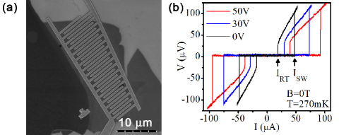
Graphene flakes are deposited on 280 nm thick SiO2 surface using mechanical exfoliation Novoselov-05 . Raman spectroscopy is used to confirm the number of layers Raman2 . The electrodes, which have a fingered shape (Fig. 1a), are patterned from a bilayer Pd/Pb (4nm/100nm), as explained in the supplementary materials (SM). In order to measure the switching current distribution, the amplitude of the sinusoidal current bias is set somewhat higher than the maximum switching current, and it is adjusted when needed to keep the sweep speed roughly constant. The number of switching events for each distribution was either 5000 (for the sample 111s) or 10000 (for the sample 105). At low temperatures the - curves of the samples exhibit a hysteretic behavior, Fig. 1b, which enables us to study switching current statistics.
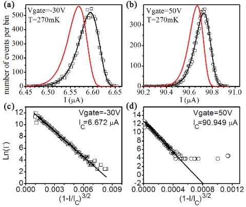
Our main focus is on the function. Figure 2 shows a switching histogram for sample 105 at (a) Dirac point () and (b) . During the experiment, some anomalously premature switching events are recorded. These events, which significantly deviate from the general population of the distribution, are very rare and are believed to be unrelated to thermal fluctuations. In order to exclude these anomalous jumps from the standard deviation calculation we first convert the raw data to the switching rate according to the Kurkijarvi method JK ; FD . The Kramers and Stewart-McCumber theories combined (see below) lead to the expectation that . In Figs. 2c and 2d we plot versus . The critical current is tuned to make the graph as linear as possible. Then the linear part of the graph is fit with a straight line. Hollow squares and circles are the measured data. Filled symbols are those points which were used to find the best linear fits. The best fit is then used to regenerate the distribution of by inverting the Kurkijärvi transformation. The results are shown as black curves in Fig. 2a and Fig. 2b, for the experimental sweep rates were A/s and mA/s. The red curves are computed distributions for A/s and mA/s correspondingly. The dispersion is then computed for the same value of for all temperatures.
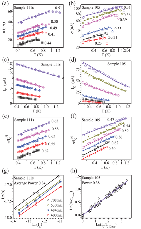
Our main results are presented in Fig. 3. This figure shows standard deviation and critical current versus temperature for various gate voltages. Figures 3a and 3b are log-log plots of versus . The best linear fit provides , which is defined by the equation . The estimated error or uncertainty in the power values is about 7. Overall, the best fit ’s are different from the theoretically predicted JJ value . Since numerous previous experiments on JJs established the power close to 2/3 while our data indicate powers roughly between 1/3 and 1/2, an understanding of such discrepancy is desirable.
We interpret these observations based on the following model. Since the pioneering theoretical work of Kurkijärvi JK and its experimental confirmation by Fulton and Dunkleberger FD kinetics of stochastic phase slips in the JJs is described within Stewart-McCumber model SM , which employs sinusoidal current-phase relation (CPR), , and represents the total current as a sum of superconducting, normal and displacement components. At the mesoscopic scale and, in particular, in the context of graphene proximity circuits, there are reasons to question the applicability of such model given the possibility of a highly nontrivial structure of (see SM). This naturally raises a question about the universality of the previous results with respect to the form of the CPR. It is rather remarkable to realize that the predictions of the theory JK in fact extend beyond the limits of its original validity. We now proceed to the generalization of the Kurkijärvi’s theory JK developed for the statistics of thermally activated phase slips in a flux-biased rf-SQUID to the case of a current-biased weak link with an arbitrary CPR.
Within the Stewart-McCumber model the dynamics of the phase is equivalent to the dynamics of a viscous Brownian particle subject to the following external potential:
| (1) |
which is the Gibbs potential. Here is the free energy and is the bias current. We assume that is a single-valued smooth function. For , is a periodic function of with alternating local maxima and minima. In the absence of fluctuations the phase is trapped in one of the minima as long as , which is a state with zero voltage. In the resistive state when the phase increases with time. In the presence of thermal fluctuations even at the phase can escape its local minimum, i.e. experience a phase slip, which drives the junction into a phase-running resistive state. Such a process is detected as a voltage jump (a switching event) on the - curve. Upon decreasing the junction may show hysteretic behavior and the quality factor determines the width of the hysteretic region. The activation rate of a phase slip for a moderately underdamped () to overdamped () junction is given by Kramers theory Kramers (hereafter )
| (2) |
The energy barrier is the spacing between two consecutive extrema: . The prefactor is determined by the curvature of the potential at minimum, and by the damping parameter , where and are effective normal resistance and capacitance of the junction. Notice that where is plasma frequency.
To find the activation barrier let us introduce a critical phase defined through . In the vicinity of one can use Taylor expansion provided is a smooth function. is obtained by integrating the supercurrent over the phase, which gives , where and . These equations determine the locations of the two consecutive extrema of the Gibbs potential: . Using Eq. (1) one finds
| (3) |
The curvature of the Gibbs potential at the extrema points can be obtained in a similar way and is given by .
The knowledge of the decay rate (Eq. 2) allows one to determine the probability that a phase slip occurred by the time , which reads: , where . Note that the probability of not having a phase slip by the time is . For a constant bias current sweep the probability can be evaluated analytically. Introducing reduced current variable and recalling the definition of the quality factor one obtains the following expression:
| (4) |
This result for the probability of a phase slip holds for a moderate to high damping provided , the condition which is very well satisfied in most of our measurements. In the limit of high damping when and one recovers the result of JK .
To evaluate the dispersion of the switching current we notice that the probability distribution of a variable is obtained from by the differentiation with respect to i.e. . Given the relation between the bias current and the reduced current this implies that the dispersions of these variables are related as . The crucial observation is that dispersion considered as a function of is constant within a few percent while is varied by several orders of magnitude, so that for all practical purposes is temperature independent JK . Using Eq. (3) and assuming that the temperature scalings of and are the same we obtain the following temperature scaling for the dispersion of switching current:
| (5) |
where is the flux quantum. Eq. (5) is the main result of the calculation, which describes the temperature dependence of for any smooth CPR. According to Eq. (5) the power of in the temperature scaling for is only expected if . In the SGS junctions the critical current keeps increasing down to the very low temperatures (Fig. 3c and 3d), due to the divergence of the normal metal coherence length in graphene, thus leading to the stronger proximity effect. The solid lines in the figures are the fits to the SNS junction theory ZZ . The fitting parameters for the theoretical fits are mean free path =-nm, which is similar to previously reported values Heersche-Nature07 ; Miao-Science07 ; Du-PRB08 , and the normal resistance , which is of the same order of magnitude as the one measured directly.
To further confirm our conclusions we plot versus the temperature as suggested by Eq. (5). The results are shown in Fig. 3e and 3f. Such critical-current-normalized dispersion obeys the power law with the power close to . For sample 105, the power rests between and ; for sample 111s these values vary between and , which are close to , predicted by the adopted Kurkijärvi model.
Another type of scaling which is suggested by Eq. (5) and which can be accessed experimentally is the dependence of the dispersion on the critical current at constant temperature. Doping-dependent conductivity of graphene provides a unique possibility to vary the critical current while keeping the temperature constant - an experimental “knob” which is inaccessible for other types of junctions.
In Figs. 3g and 3h we present results of such measurements. We plot the versus for various temperatures (Fig. 3g) and scaled versus scaled (Fig. 3h). The average value of the power for sample 111s is 0.34. The power of scaled data for sample 105 is 0.38, which is shown as the best fit of the data. The resulting powers are very close to the theoretically expected value of 1/3.
In summary, we have studied the dispersion of the switching current distribution in moderately underdamped SGS junctions with clear hysteretic - characteristics. A systematic measurements of both temperature and critical current scaling (at constant ) of the dispersion is performed. The latter study, unavailable in regular junctions, is made possible by a gate-voltage-tuned conductivity of graphene. The temperature scaling of the switching dispersion shows unusual power laws, which is explained theoretically by taking into account the temperature variation of the critical current. The critical current scaling of the dispersion is explained theoretically by combined Stewart-McCumber and Kurkijärvi models, and is applicable for the mesoscopic junctions with arbitrary current-phase relationships.
The work was supported by ONR grant N000140910689. V.V. was supported by the Center for Emergent Superconductivity funded by DOE, under Award No. DE-AC0298CH1088.
References
- (1) K. S. Novoselov, et al., Nature 438, 197 (2005).
- (2) Y. Zhang, et al., Nature 438, 201 (2005).
- (3) A. K. Geim and K. S. Novoselov, Nat. Mater. 6, 183 (2007).
- (4) A. K. Geim, Science 324, 1530 (2009).
- (5) A. H. Castro Neto, et al., Rev. Mod. Phys. 81, 109 (2009).
- (6) C. W. J. Beenakker, Phys. Rev. Lett. 97, 067007 (2006); Rev. Mod. Phys. 80, 1337 (2008).
- (7) H. Meissner, Phys. Rev. Lett. 2, 458 (1959).
- (8) H. B. Heersche, et al., Nature 446, 56 (2007).
- (9) F. Miao, et al., Science 317, 1530 (2007).
- (10) X. Du, I. Skachko, and E. Y. Andrei, Phys. Rev. B 77, 184507 (2008).
- (11) C. M. Ojeda-Aristizabal, et al., Phys. Rev. B 79, 165436 (2009).
- (12) D. Jeong, et al., Phys. Rev. B 83, 094503 (2011).
- (13) I. V. Borzenets, et al., Phys. Rev. Lett. 107, 137005 (2011).
- (14) G. H. Lee, et al., Phys. Rev. Lett. 107, 146605 (2011) .
- (15) J. M. Martinis, M. H. Devoret, and J. Clarke, Phys. Rev. B 35, 4682 (1987).
- (16) M. Sahu, et al., Nature Physics 5, 503 (2009); P. Li, et al., Phys. Rev. Lett. 107, 137004 (2011).
- (17) H. F. Yu, et al., Phys. Rev. Lett. 107, 067004 (2011).
- (18) P.A. Warburton, et al., Phys. Rev. Lett. 103, 217002 (2009).
- (19) T. A. Fulton and L. N. Dunkleberger, Phys. Rev. B 9, 4760 (1974).
- (20) J. Kurkijärvi, Phys. Rev. B 6, 832 (1972).
- (21) D. Graf et al., Nano Letters 7, 238 (2007).
- (22) M. Tinkahm, Introduction to Superconductivity, 2d ed. (McGraw-Hill Inc. 1996).
- (23) W. C. Stewart, Appl. Phys. Lett. 12, 277 (1968); D. E. McCumber, J. Appl. Phys. 39, 3133 (1968).
- (24) H.A. Kramers, Physica 7, 284 (1940).
- (25) A. D. Zaikin and G. F. Zharkov, Sov. J. Low. Temp. Phys. 7(3), 184 (1981); P. Dubos et al., Phys. Rev. B 63, 064502 (2001).
Appendix A Supplementary Materials
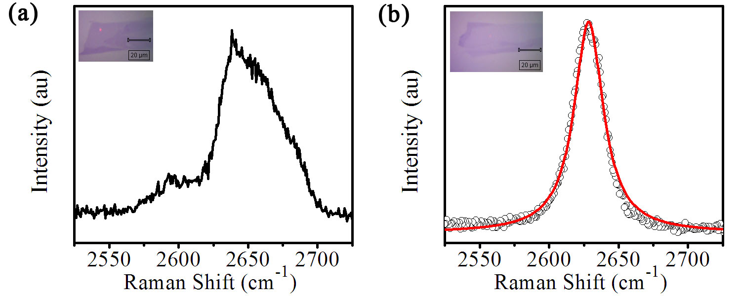
Raman spectra and additional sample preparation details.– In Fig. 4, the Raman spectroscopy results are plotted for two different thin graphite flakes. In the thicker flake, the peak profile is non-Lorentzian and shows a small side peak. In addition, the FWHM of the best fit Lorenzian is 33 cm-1. However, in the thin flake, the peak profile is Lorentzian and located between and cm-1. In addition, the FWHM for this sample is 13 cm-1, which is suggestive that the thin flake is graphene Raman3 .
A pair of pseudo-four-probe electrodes are patterned using ebeam lithography. In a thermal evaporator, a layer of 4nm Pd is evaporated at a rate of 0.5-1.0 A/s as slower evaporation rates would lead to a high contact resistance, possibly due to heating of the graphene by radiation coming from the molten target. Following the first layer, a layer of 100 nm Pb is evaporated at a rate of 10-30 A/s. We have found that a faster Pb evaporation provides more uniform films, thus it is desirable. We have used a liquid nitrogen trap to remove the residual contaminants in the chamber and thus to increase the quality of the films. After evaporation, the sample is placed in a hot acetone bath for total 5 minutes for the lift-off step. While being in the acetone bath, the sample is sonicated for 10 seconds every other minute. The sample is kept in the second bath of acetone for 5 minutes before it is rinsed with iso-propanol and dried. The Pb electrodes are too soft to use wire bonder thus indium dots have been used to connect the leads to the chip. The sample is measured in a He3 system. The system is equipped with room temperature of Pi Filters and low temperature Cu powder filter.
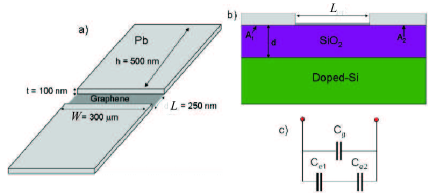
Remarks on junction capacitance.– Total capacitance is an important characteristic of the junctions. It defines quality factor which in a way determines whether junction’s dynamics is overdamped or underdamped. In the main text we determined from the experimental values of the critical and retrapping currents, which together with the junction’s normal resistance provided us an estimate for . An alternative way to determine is suggested by considering the geometry of our sample, see Fig. 5. An estimate of the capacitance across the graphene sheet can be found with the help of the formula for coplanar electrodes Song-APL70 : , which leads us to the conclusion that the electrode capacitance should be fF. Here is the permittivity of free space, is the relative permittivity of silicon , is the junction width m, and is the complete elliptical integral of modulus ; is the distance between electrodes. Note, however, that two electrodes have an additional capacitive coupling through the gate. Thus Fig. 5b gives the proper geometry and electrical scheme for the calculation of the full capacitance across the junction. In this geometry, is nm, and the area of each electrode (including the presence of a pressed indium dot to facilitate the electrical connection to the pins on the chip carrier) is and m2. Thus the capacitance of each electrode to the gate is and pF, which is calculated from the formula , where is the distance to the substrate. Using the circuit scheme as in Fig. 5c, the total capacitance is found to be pF, which is in between the values that can be determined from the quality factor argument. Indeed, for mK, the quality factor was found to vary between 3.5 and 4.2 for the entire range of gate voltages from the values of and . Thus the SGS junction (sample 105) is moderately underdamped as it is larger than 0.84. Since the quality factor is where , we calculate that the capacitance of the sample varies between 12 pF and 50 pF. This consideration proves consistency of our estimates between two independent approaches, and confirms the conclusion that our SGS junction is in the underdamped regime.
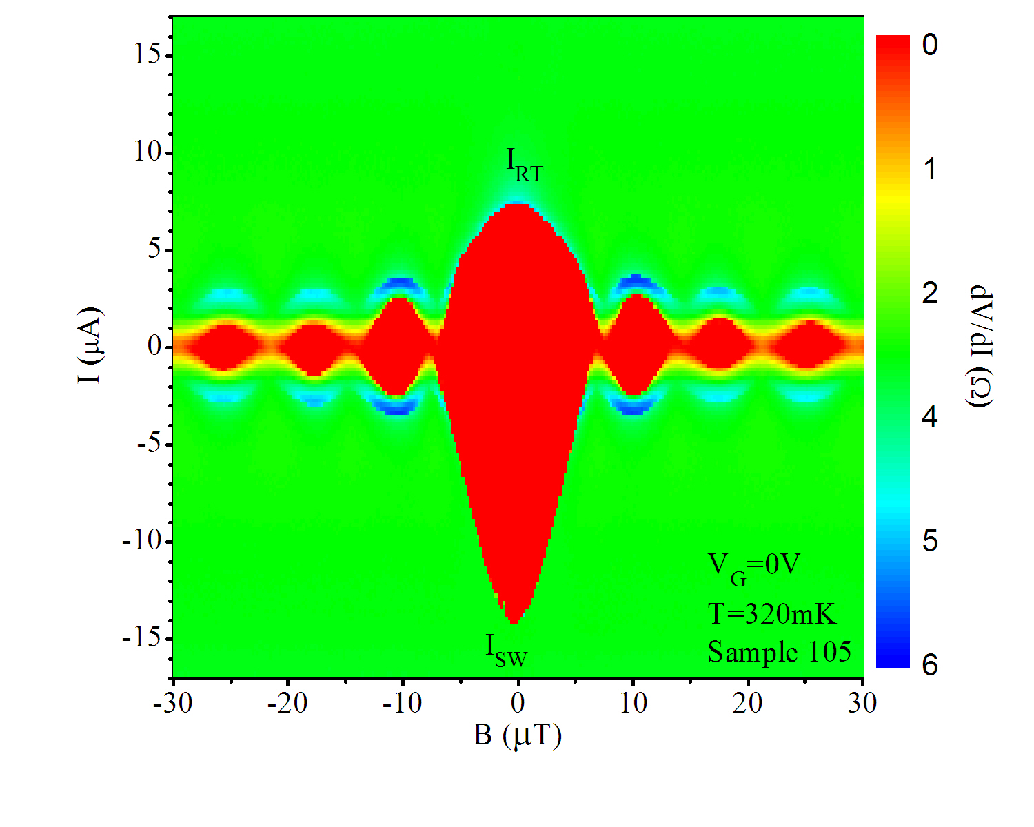
Characterization of graphene proximity junctions.– In this section, the basic characterization of the electronic transport properties of graphene proximity junctions will be presented. We focus mainly on the magnetic field dependence of the supercurrent, which demonstrates high quality JJ in our graphene based devise, and on the gate voltage dependence of resistance and switching current, which traces properties of the graphene, associated with the Dirac spectrum. This discussion complements presentation given in the main text.
The magnetic field dependence of the switching current can be measured and compared to Josephson junction theory. In an extended JJ, the maximum (or critical) current as the function of applied magnetic flux can be fit to a Fraunhofer function:
| (6) |
where is the magnetic flux through the junction which is given by , is the magnetic field, and is the magnetic flux quantum. The effective area is larger than just due to the magnetic field penetration into the electrodes by a distance equal to the penetration depth .
The fit of our data to the Fraunhofer pattern can be seen in Fig. 1d of the main text, where a good fit is obtained using an area that is estimated from the junction area of m2, which results in a magnetic field period of mT. A vertical shift of mA was also used to obtain the fit to account for the supercurrent observed even at the Dirac point. The magnetic field period obtained from the experimental data is somewhat small at about mT. This discrepancy between the fitted and measured value can be traced to an understanding of the effective area of the junction . Using a penetration depth of nm results in an effect area of m2 and a magnetic field period of mT. If the area of the entire electrode plus junction were used, the magnetic field period would be mT. Thus, to fit to the Fraunhofer period the penetration depth in our samples should be larger than nm in order to increase the effective area of the junction. The differential resistance of the junction can also be measured as a function of bias current and magnetic field, see Fig. 6. Again, the Fraunhofer pattern is observed, with a slightly reduced value of the switching current even at a applied gate voltage of V due to a shift of the Dirac point after the thermal cycling.
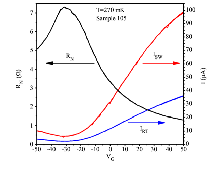
The switching current and resistance as a function of the gate voltage are displayed in Fig. 7. As the gate voltage is swept away from the Dirac point, the total carrier concentration increases and thus, the switching current is expected to increase as well, which is confirmed in Fig. 7a. Similarly, the retrapping current increases as well. In addition, the resistance of the sample decreases as the carrier concentration increases. In Fig. 7a the Dirac point is observed to be at V and above this value the Fermi energy is shifted to the conduction band and thus the charge carriers are primarily electrons while below V, the Fermi energy is shifted to the valence band and the charge carriers are mostly holes. Thus, this figure confirms that our junctions are capable of carrying a bipolar supercurrent. It is also clear that the gate voltage can be used to tune the critical current of our graphene proximity junctions, which can be used as a tool to study the escape dynamics.
Current-phase relation in graphene and .– Although detailed information about CPR in the SGS proximity junction was not needed for our analysis of current switching statistics, nevertheless, we provide such information for completeness. The equilibrium Josephson current can be found from the thermodynamic relation
| (7) |
by knowing free energy as a function of the phase difference across the junction. Bardeen et. al. Bardeen-PR69 derived general expression for with the help of Bogolubov-de Gennes (BdG) equations, which reads
| (8) |
This result is a generalization of that used in BCS model for the case of . The sum over is just what would be obtained for the free energy for an assembly of independent fermions with energies . As in the Hartree-Fock approximation, this counts the interaction energy twice. The next term, , the negative of the interaction energy, corrects for this double counting. Since the bulk energy is independent of the phase one obtains from Eq. (8) after differentiation
| (9) |
where we have rewritten sum over as a sum over the discrete positive eigenvalues of BdG equations, and an integration over the continuous spectrum with density of states . The additional factor of in the above formula, as compared to the conventional expression, accounts for two valleys in graphene. Although above the gap states, , do contribute to the Josephson current AL their role, in fact, is subleading as compared to the contribution coming from the Andreev bounds states with energies below the gap . One thus only need to consider the first term in Eq. (9). In the context of graphene the spectrum of Andreev levels can be found from the BdG equations in the following form Titov-PRB06
| (10) |
where is electron(hole) wave functions combined in the vector, dot product is defined in the conventional way , symbol stands for the direct product between matrices, which operate in the isospin () and electron-hole () spaces. Chemical potential is measured with respect to Dirac point, so that corresponds to undoped graphene. Electron-like and hole-like wave functions are related to each other at the SG interfaces via specular reflection Andreev processes. Mathematically this can be represented as follows Titov-PRB06
| (11a) | |||
| (11b) |
Assuming hard wall boundary conditions in the -direction -component of particle wave vector becomes quantized . Performing then Fourier transform in Eq. (10), matching electron/hole plane waves at both interfaces with the help of boundary conditions (11) and setting determinant of the corresponding matrix equation to zero one finds
| (12) |
which determines dispersion relation for the Andreev levels, where , , . The last equation can be resolved analytically for as the function of the channel index and superconducting phase difference in the form
| (13) |
where has meaning of the transmission coefficient in the transversal channel, which is given explicitly by
| (14) |
with . Note that at the Dirac point, , all channels are evanescent, since and thus
| (15) |
Having determined the spectrum of energy states below the gap we can return to Eq. (9) and find Josephson current in the form Cserti-PRB10
| (16) |
where should be taken from Eq. (13). In the vicinity of the neutrality point, , where is ballistic Thouless energy, to the good approximation one can use Eq. (15) for the transmission coefficient. Furthermore, if the aspect ratio of graphene sheet is such that then summation over discrete can be replaced by the integration with . Introducing also dimensionless variable one arrives at
| (17) |
There is no close analytical expression for this integral, except for the zero temperature limit, when . In that case Titov-PRB06 ; KO
| (18) |
which coincides with the result of Kulik-Omelyanchuk for the case of disordered SNS junction KO . This is rather peculiar result since calculation was done for the manifestly ballistic limit of graphene. From the CPR we can restore free energy barrier for phase slips and thus hight of the Gibbs potential (see Eq. 3 in the main text):
| (19) |
where we have used , , with , and which corresponds to the maximum of . For completeness we mention that in the longer junctions, , all transmissions are exponentially suppressed, , such that summation reduced to the geometrical progression to the leading order in , with the result
| (20) |
Note that for our samples the aspect ratio is at least so that Eqs. (18)–(19) should apply near the neutrality point.
At the relatively high doping when full expression for is needed for the calculation of . Although there is no close analytical expression for the CPR in this case, critical Josephson current can be estimates as
| (21) |
where has meaning of the number of propagating transversal channels. All above considerations apply, strictly speaking, to the short junctions in the sense of the proximity effect, where is superconducting coherence length. Note, however, that our SGS devices are rather at the crossover between long and short limits with the typical ratio .
Surprisingly, we do not find solid experimental evidence in support of ballistic transport in the SGS proximity junctions. All aspects of our data, and in particular temperature and gate voltage dependence of the critical current, are in fact in good quantitative agreement with the predictions of diffusive SNS junction model AL ; ZZ-app ; Dubos-PRB01-App . Specifically we use
| (22) |
to fit the experimental data (see Fig. 3c and 3d of the main text). In Eq. (22) , and . In theory Eq. (22) applies at , where is diffusive Thouless energy and is diffusion coefficient. For the typical parameters of our samples m/s, nm, nm one finds K which corresponds to for the working temperature regime K. Note also that as shown in the extensive study of Ref. Dubos-PRB01-App , Eq. (22) works well in the rather wide temperature range. At the lowest temperatures, , critical current saturates with the exponential accuracy AL ; Dubos-PRB01-App
| (23) |
where , , and . Finally, one should note that product (up to a numerical factor of order one) sets the magnitude of the Gibbs barrier for the phase slips. For example, at K in the case of sample 105 taking the corresponding values and one estimates K, such that in agreement with our earlier discussions in the main text.
References
- (1) D. Graf et. al., Nano Letters 7, 238 (2007).
- (2) Y. Song, J. Appl. Phys. 47, 2651 (1976).
- (3) J. Bardeen, R. Kümmel, A. E. Jacobs, and L. Tewordt, Phys. Rev. 187, 556 (1969).
- (4) A. Levchenko, A. Kamenev, and L. Glazman, Phys. Rev. B 74, 212509 (2006); Phys. Rev. B 77, 180503(R) (2008).
- (5) M. Titov and C. W. J. Beenakker, Phys. Rev. B 74, 041401(R) (2006).
- (6) I. Hagymási, A. Kormányos, and J. Cserti, Phys. Rev. B 82, 134516 (2010).
- (7) I. O. Kulik and A. N. Omelyanchuk, JETP Lett. 21, 96 (1975).
- (8) A. D. Zaikin and G. F. Zharkov, Sov. J. Low. Temp. Phys. 7(3), 184 (1981).
- (9) P. Dubos et. al., Phys. Rev. B 63, 064502 (2001).