Retrapping Current, Self-Heating, and Hysteretic Current-Voltage Curves
in
Ultra-Narrow Superconducting Aluminum Nanowires
Abstract
Hysteretic I-V (current-voltage) is studied in narrow Al nanowires. The nanowires have a cross section as small as 50 . We focus on the retapping current in a down-sweep of the current, at which a nanowire re-enters the superconducting state from a normal state. The retrapping current is found to be significantly smaller than the switching current at which the nanowire switches into the normal state from a superconducting state during a current up-sweep. For wires of different lengths, we analyze the heat removal due to various processes, including electronic and phonon processes. For a short wires in length, electronic thermal conduction is effective; for longer wires in length, phonon conduction becomes important. We demonstrate that the measured retrapping current as a function of temperature can be quantitatively accounted for by the self-heating occurring in the normal portions of the nanowires to better than 20 % accuracy. For the phonon processes, the extracted thermal conduction parameters support the notion of a reduced phase-space below 3-dimensions, consistent with the phonon thermal wavelength having exceeded the lateral dimensions at temperatures below . Nevertheless, surprisingly the best fit was achieved with a functional form corresponding to 3-dimensional phonons, albeit requiring parameters far exceeding known values in the literature.
pacs:
Valid PACS appear hereUnderstanding the dynamics of ultra narrow supeconducting (SC) nanowire wires is an active area of investigation Giordano.PRL ; Nature ; Lau.PRL ; Highfield.B ; Fabio.PRL ; HysteresisIV ; NaturePhysics ; PengPRL ; Goldbart ; Little ; LA ; MH ; QPStheory.Zaikin1 ; QPStheory.Zaikin2 ; sergei . A significant focus is the so- called 1-dimensional (1D) limit, delineated by the condition, , where w is the width and h the height of the nanowire, and the superconducting coherence length. Investigations of the behavior under current-biasing not only elucidate the conditions and limitations for the current carrying capabilities, as well as the process of recovery back into the superconducting (SC) state after driven normal by an excessive current, but also potentially lay the foundation and pave the way for the development of novel devices, such as a current-Josephson effect devices CurrentJJ , or qubits nanowire.qbit .
In this work, we report on measurements carried out in ultra narrow Al nanowires with a cross section as small as 50 . The three nanowires studied have a widths and heights ranging between 7 - 10 , and lengths of 1.5 (wire S1) or 10 (wires S2, S4). These nanowires are exceedingly uniform in their cross section, as indicated by their ability to carry sizable current before being driven normal, where the current density is nearly identical to co-evaporated 2d films. In a previous work, the behavior of the switching current during an up-sweep of the current was investigated PengPRL . There, it was found that heat deposited by phase-slips– transient temporal-spatial events during which the superconducting phase fluctuates and changes by over a distance of order , while the core region goes normal–leads to a thermal runaway, driving the entire nanowire into a normal state from the SC state.
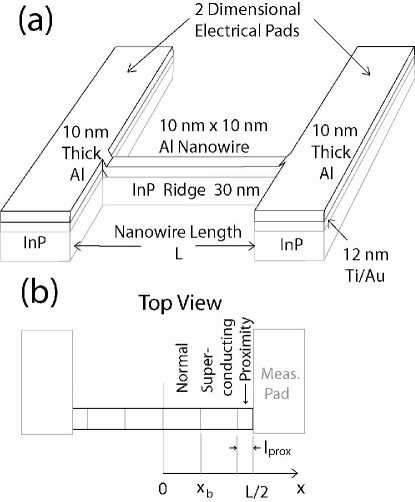
Here we focus on the down-sweep retrapping current. The retrapping current is found to be significantly smaller than the up-sweep switching current , and can be a much as a factor of 20 smaller. The history dependent current-voltage (IV) relation exemplified by the disparate behaviors in the up- and down-sweep is ubiquitous, despite the fact that based on the criteria normally applied to SNS (superconductor-normal metal- superconductor) bridges, the nanowires should be in the heavily over-damped regime in its dynamics HysteresisIV ; NaturePhysics ; Hysteresis.SNS . In nanowires of widths , Tinkham et al.HysteresisIV performed a heat flow analysis, and ascribed the retrapping behavior to self-heating. Our work bears similarity to that work, but our SC nanowires are in a different regime, where , rather than being close to 1 in their case. Here is the Fermi wave-number, and is the mean-free-path. Moreover, their nanowires were suspended freely, while ours are deposited onto a narrow, 8 nm-wide InP ridge (Fig. 1(a)), and are thus in thermal contact with an underlying substrate. Furthermore, our analysis differs from theirs in the form of the heat flow equations. Based on our analysis, we rule out under-damping as the cause of the hysteresis, in agreement with recent results in submicron SNS bridges Hysteresis.SNS .
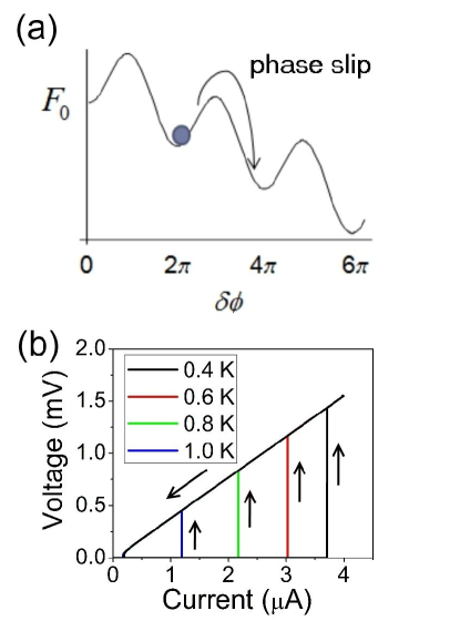
To lay the framework for understanding the behavior of nanowires, the Josephson junction can serve as a starting point. There, the free energy landscape under current bias is described by the tilted washboard potential, shown in Fig. 2(a) TinkhamBook . This same scenario is also applicable to 1D SC nanowires LA ; MH . Josephson junctions are classified within a Resistively and Capacitively Shunted Junction (RCSJ) model as either under- or over-damped, depending on whether the quality factor, , is greater or less than 1. Here, is the critical Josephson current, C is the junction capacitance, and R the junction normal state resistance. When under-damped Josephson junction is driven over the free-energy barrier out of its meta-stable minimum, the SC phase keeps running downhill as there is insufficient damping to retrap the phase in a lower energy local minimum. A consequence is that a hysteretic current-voltage (IV) relation, where the up-sweep and down-sweep branches do not overlap. In contrast, in an over-damped junction, the phase moves diffusively between adjacent minima, and hysteresis is often not present MQT.Clarke ; Collapse1 ; Collapse2 .
The estimated for our nanowiresis in the range of , far below unity, and the nanowires are ostensibly in the severely over-damped limit. This estimate is relevant when the nanowire device is in the S-NW-S configuration, where S refers to each of the two large metallic measurement pads when in the SC state, and NW denotes the nanowire. It also provides a reasonable estimate in the N-NW-N configuration, when the pads are driven normal, but the ambient temperature is below the nanowire SC transition temperature . In this case, the nanowire itself breaks up into alternating SC and normal segments, whether during an upsweep or a downsweep of the current. In the former case, the nanowire is overall in the SC state, but during a phase-slip, the phase-slip normal core acts as the normal region. In the latter, the central portion of the nanowire is normal due to heating, while the regions closer to the pads are in the SC state (Fig. 1(b)).
Nevertheless, despite the over-damping, hysteretic IV curves are ubiquitous, as can be seen for wire S2 in Fig. 2(a). In fact, the ratio of to can be as small as . For example, in nanowire S2 at , , while . These observations motivated us to investigate the retrapping current systematically, as a function of the temperature and wire length, and to perform a detailed heat analysis to establish self-heating as a cause of the substantially reduced below the value of the upsweep .
Our devices were fabricated using a template method. The template is a narrow, wide InP ridge, formed by differential etching on the cleaved (110) crystallographic plane of a molecular-beam-epitaxy (MBE) grown InGaAs-InP crystal, where the growth direction is (001). The geometry of our devices is depicted in Fig. 1(a). The details of the fabrication procedure is described in a previous work Fabio.APL . The nanowire resides on the narrow InP ridge and is thus thermally connected to the large semiconductor substrate through the narrow ridge. The nanowire is electrically connected to large metallic measurement pads on its ends. Therefore, for heat removal, thermal conduction both in the lateral direction along the nanowire, and vertically through the InP ridge via phonon processes must be considered. The IV measurements were carried out in a extremely carefully shielded apparatus to minimize unwanted environmental interference, such as external noise (e.g. from nearby radio stations) conducted down the electrical cables, or Johnson-Nyquist noise from resistors within the electrical measurement circuitry. In particular, Thermax cables with the ability to remove high frequency noise is employed where possible, as well as low-temperature RF filters. The devices are also enclosed in metal cans with all openings plugged with conductive tape or metal mesh.
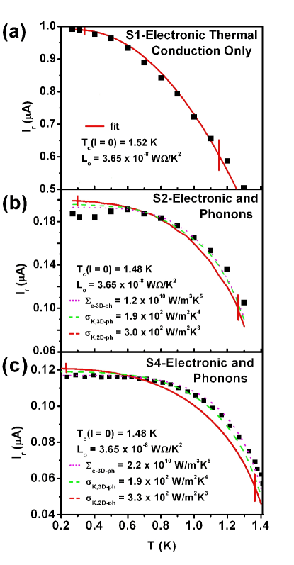
In Fig. 3(a)-(c), we present the measured for the three nanowires S1 (), S2 (), and S4 (), respectively, as a function of temperature. Immediately apparent is the substantial difference in the magnitude of the retrapping current for the short S1, when compared to the longer S2 and S4. For S1, at , while it is and , respectively for S2 and S4. Thus, the value of in S1 is roughly 5 - 8 times that in S2 or S4. The results for S2 and S4 do not depend on whether measurements were carried out in the S-NW-S or the N-NW-N configuration. On the other hand, for S1, due to the larger current level and associated excessive heating, it was necessary to drive the measurement pads into a normal state, into the N-NW-N configuration. By driving these pads into the normal state using a small magnetic field , the now normal pads can act as good thermal anchors, keeping the temperatures of the ends at the ambient temperature . For the longer S2 and S4, the smaller current level means that a much lower amount of heat needs to be carried out through wire ends; thus improved thermal anchoring was not needed. For S1, on the other hand, keeping the pads SC (S-NW-S configuration) reduced to from as heat removal becomes more difficult due to poor thermal conduction capability of the SC pads. At the same time, instabilities arise in the temperature profile along the nanowire, leading to very noisy data below with fluctuating as much as between adjacent data points.
The configuration with normal electrical pads is relevant for our data in Fig. 3. In the analysis which follows, we will focus on this configuration. The retrapping process returns a nanowire into the SC state during a down-sweep of the current, , at an ambient lattice temperature, , below the zero current critical temperature, . At large , most of the nanowire remains normal due to self-heating, which raises the local temperature above the switching temperature at that current, .
During a current downsweep, the temperature is position dependent along the nanowire. In the N-NW-N configuration, each of its ends is connected to a large, normal metal electrical measurement pads, anchored at . Because , and is in fact below , the end regions are in the SC state, aside from a short proximity region, in length, immediately adjacent to each normal pad (Figs. 1(b)). Here, the is the upsweep switching temperature at current , On the other hand, as long as exceeded , the center of the nanowire is above and is thus in the normal state. When is reduced down to , a blockage preventing the central region to be cooled is suddenly removed, allowing the cooling to propagate all the way to the center. This blockage removal is described in detail in what follows.
The upsweep switching temperature for a given current expresses the same relation as the switch current as a function of temperature , but viewed in reverse. For our nanowires, these were reported in Ref. 8 PengPRL . It is worthwhile to point out that the value of at a given temperature is not unique, but depends on the upsweep ramp rate of the current. Conversely, is also dependent on the ramp rate. This is due to the fact that the switching is caused by phase-slip events Goldbart ; NaturePhysics ; PengPRL , and thus the relative rates of the phase-slip generation to current upsweep matters. The slower the upsweep current ramp rate, the longer waiting time is available for phase-slip events to take place within a given interval in current. This increases the probability for switching within that interval and reduces the magnitude of the current at which switching takes place. But because the rate of phase-slip generation is exponentially dependent on the current, the dependence of on ramp rate is weak, and is approximately logarithmic.
To estimate , it is necessary to determine the position dependent temperature, . Both the electronic and phonon thermal conduction mechanisms need to be considered. The temperature range of interest is low compared to the lattice DeBeye temperature and the temperature dependence of the phonon thermal conductivity takes a power-law form, reflecting the phonon density of states. At these low temperatures, , the value of the phonon conductivity is considerably smaller than the electronic thermal conductivity. The only exception is in the SC regions when . Thus, in the absence of a very large temperature rise phonons can only carry away a relatively small amount of heat. Whereas electronic conduction requires the heat to exit the ends of the nanowire, the phonon conduction goes through the short InP template ridge (in height), on which the nanowire resides. The nanowire length is microns while the ridge is only in height. If the wire is long, the electronic mechanism will become much less effective, and phonon conduction must be included as well.
For the short wire S1, electronic conduction overwhelmingly dominates. For the long wire S2, both electronic and phonon thermal conduction must take place side by side. Phonon conduction through the InP ridge takes place via several steps: (a) electron-phonon energy relaxation within the aluminum nanowire, (b) conduction through the aluminum-InP boundary, and (c) conduction through the 8 nm wide, 30 nm tall InP ridge. Below the ridge, the energy is dissipated in the very highly conductive GaAs bulk material. Thus the base of the InP ridge can safely be assumed to be held at the ambient temperature, .
One additional mechanism of heat removal takes place through the liquid , which surrounded the nanowires in the set of measurement on S1 and S2. However, this channel appears less important. Additional data for wire S4 obtained in the dilution refrigerator, in which the samples are in vacuum and thus there is no liquid surrounding the nanowire, yielded a retrapping current which can be accounted for in a similar manner as S2, using electronic and InP ridge thermal conduction only. Note both wires S2 and S4 are in length.
We divide a nanowire into two symmetric halves of length each, where is the total wire length, and consider the right half, where , and , as shown in Fig. 1(b). When slowly down-sweeping the current , we assume that the nanowire is in the SC state at a position , if , but is in a normal state if .
We begin by considering the short wire S1 ( in length) and only include electronic conduction. Phonon conduction alone will remove of the heat generated by heating, and will be neglected. The diffusion equations must account for three regions: (a) the central region for , which is normal for and has a resistance per unit length of PengPRL and thus self-heats; (b) the SC segment for , which nearly does not self heat, but must conduct the heat generated by the central normal segment, and (c) the short proximity region adjacent to the normal metal pads for which is approximated as a normal region. More precisely, the SC region close to the SC-normal boundary heats slightly due to occasional phase slips as its temperature is just below ; the proximity region generates self-heating, and in addition must conduct through it the heat of the central normal region as well. For the normal metal regions, the steady state heat diffusion equation is given by:
| (1) |
where is the electronic Wiedemann-Franz electronic thermal conductivity, is Lorenz number determined from fitting, and the nanowire cross sectional area. In the SC region, it is replaced by:
| (2) |
The equations in the three regions are supplemented by boundary conditions at the junctions. The junction between the center normal region and the SC region takes place at , and between the SC and short proximity regions, at . The temperature is continuous across each junction, and the heat flow is identical immediately to the left and right. Lastly, we have . Note that the forms of these equations differ from those used in Ref. 6. There, the variation of the thermal conductivity or with position, through their dependence on temperature T, was not accounted for HysteresisIV .
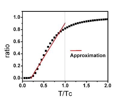
At a given temperature below , the electronic thermal conductivity of the SC segment at a position x, with a temperature , is related to the corresponding normal metal W-F thermal conductivity at that temperature, by the ratio :Hysteresis.SNS
| (3) |
This integral evaluated numerically is shown in Fig. 4. For the purpose of determining the position dependent temperature at a given , this ratio is approximated by a linear form as indicated in the figure for :
| (4) |
We next describe how the cooling blockage can be removed, and determine the condition for this to occur. To do so, we consider the SC region and fix the current at . The SC-normal boundary occurs at , which is determined by equating the temperature at , , to the switching temperature at that current . Momentarily treating as a variable, attains its maximum value at a critical value ; in the simplest approximation is independent of as will be seen below. For a large current , the normal region is large and the actual exceeds (Fig. 5). As is reduced down to , the normal region shrinks and becomes equal to . Here, takes on the maximum possible value at , since , and is equal to . Further reducing to just below , will slightly increase from , while at every , will slightly decrease due to reduced heating. The decreased maximum temperature at , , can no longer reach the increased . The boundary will become unstable, and will propagate toward the center at . Starting from the inital boundary at , more and more of the normal region will fall below and become superconducting, as the shrinking normal region generates less and less heat, until the entire wire is cooled. The three cases are depicted in Fig. 5.
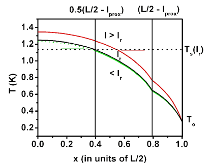
The value for can be deduced from the steady-state heat diffusion equation in the SC state, Eq. 2. Neglecting the short proximity region adjacent to the pad, (); accounting for the proximity region of length modifies this to . For illustrative purposes, let us determine in the absence of the proximity region. Focusing on the SC region at its border with the normal segment, , twice integrating the diffusion equation and matching the boundary conditions yields for the left-hand-side (LHS):
| (5) |
which is maximal for for fixed . At the factor represents the heating power generated by the normal region where . Equating the LHS to a twice-integrated right-hand-side and solving for thus yields the highest temperature at the normal-SC border when , where the LHS is maximal.
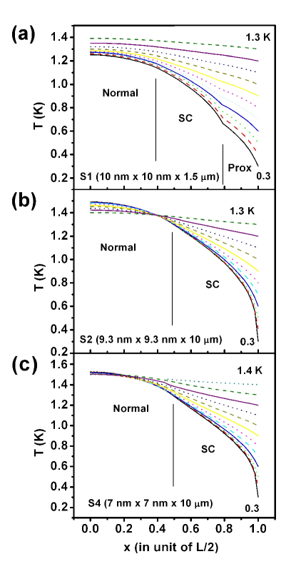
Using the approximate form of the thermal conductivity ratio between the SC and normal states given by Eq. 4, the diffusion equation can readily be solved analytically. The solution yielded the position dependent temperature profile shown in Fig. 6(a). The kink at the SC-proximity boundary is an artifact of our model, where the proximity region is approximated as a normal region. A more accurate model would require solving the Usadel equation, which is expected to yield a rounding and smoothing of the kink. See Ref. 24 for an example of the rounded voltage profile in the proximity region. The fit to the as a function of temperature is presented in Fig. 3(a), using a Lorenz number , somewhat higher that the theoretical value of . Viewed in another way, forcing to take the theoretical value, our model would predict a low temperature , rather than the we observed. Reconciling this discrepancy may require the development of more sophisticated analysis using the Usadel equation, while incorporating heating and a position dependent temperature at the same time. Despite the discrepancies, the overall behavior and magnitude (within 20 % accuracy) are captured in our simplified model.
For the wires S2 and S4, electronic thermal conduction alone is not sufficient to support the measured , despite its smaller value (by a factor of 5 - 8 at ). It is necessary to include phonon conduction. We assume a power-law temperature dependence in the heat exchange rate. At every position, the heat-removal linear power density is set proportional to , where may be varied to reflect the limiting process in the phonon conduction discussed above. The steady-state heat diffusion equation takes the forms:
| (6) |
and
| (7) |
for the normal and SC segments, respectively. For the longer wires S2 and S4, the smaller values allow the short proximity region adjacent to the normal-metal pads to be neglected.
This form for the heat-removal power-density-per-unit-length assumes that phonon conduction along the wire direction is weak–a reasonable assumption since the thermal conductivity is small, and since the wire is much longer than the height of the InP ridge (i.e. ). It also assumes that the environment to which the energy is dissipated is well-anchored at the ambient temperature. For instance, if the electron-phonon relaxation is the limiting step, it is reasonable to assume that the combination of Kapitza and InP ridge phonon conduction is sufficiently large that the phonon temperature within the nanowire is maintained at . On the other hand, if Kapitza boundary resistance limits the rate of heat removal via the phonons, then it is reasonable to assume the phonons within the InP ridge are at .
Several choices are possible for . For electron-phonon energy relaxation via 3-dimensional (3D) phonons, , while for Kapitza boundary resistance, . However, the small lateral dimensions (width and/or height) in either the nanowire or InP ridge should render the phonons reduced below 3D, down to 1D and 2D, respectively. This occurs because the thermal phonon wavelength , exceeds the lateral dimension(s) for (more precisely, ). Note that the width of the InP ridge is while the width/height of the nanowire or . By examining the fitted coefficient in front of the power-law term, one seeks to exclude various possibilities. This coefficient naturally depends on the limiting mechanism. For example, in the case of electron-3D phonon relaxation, , where is the 3D energy relaxation rate constant and the nanowire cross sectional area. For Kaptiza boundary resistance limited thermal conduction with 3D InP phonons, , where is the Kapitza boundary conductance at temperature T.
These highly nonlinear equations were solved approximately by numerical methods, yielding the position dependent temperature profiles shown in Figs. 6(b) and (c), respectively for S2 and S4. The fitting to versus temperature yielded the curves in Figs. 3(b) and (c), with fixed at the value from wire S1, of . The critical value was found to shiftly slightly toward the center, to () rather than (). The best fit is for , corresponding to the electron-3D phonon energy relaxation as the limiting step. Fits of slightly lower quality can be achieved for or . On the other hand, the numerical values for the coefficient yielded values for the parameters, which point to Kapitza boundary resistance at the Al nanowire-InP interface as the limiting path to phonon conduction.
For the extracted electron-3D-phonon relaxation rate for S2 is as large as the established value Hysteresis.SNS and is for S4. The values are thus inconsistent. We are forced to consider the possibility that the Al phonons are reduced in dimensions down to 1D. An enhancement of can be expected per dimension reduced, where is the lattice constant, yielding a factor , far larger than the measured enhancement! Instead, within this scenario, one expects the limiting step to be the Kapitza boundary resistance between the Al nanowire and the InP ridge.
For Kapitza boundary limited conduction, one may expect rather than due to reduced-dimension 2D InP phonons, despite the poorer quality fit. An enhancement factor of over the known 3D value should be present from the reduction in dimension by 1. As a reference, we use , obtained for Au on GaAs rather than Al on InP MohantyRoukes . Forcing yield the parameter value , which is 10 times the reference value. Instead, after conversion of the reference value to account for 2D phonons, the enhanced value of is consistent with the fitted values of and , respectively, for S2 and S4 (with ). To make certain this picture of Kapitza boundary limited conduction is consistent, we need to ensure the ridge phonon thermal conduction is larger. An estimate of the phonon thermal conductivity of the InP ridge itself yields a lower bound of , corresponding to the case of a very short, ridge-width limited phonon mean free path . This rules out phonon conduction in the InP ridge as the limiting step, as required. Finally, as a reference, we estimate the conductivity in the absence of any electronic contribution. This yield a value roughly double the above values for the 2D phonon Kaptiza boundary resistance coefficient.
It is worthwhile to re-emphasize the evidence for reduced dimension Kaptiza boundary conduction as the limiting step, based on a direct comparison of the fitting parameter values for S2 and S4. Whereas, for electron-phonon relaxation limited heat removal shows a discrepancy between S2 and S4 of a factor , the values for the reduced dimension for 2D InP ridge phonon, Kapitza boundary limited thermal conduction are within of each other! This, in conjunction with the discrepancy with the known reference value for , helps establish the Kapitza boundary resistance limited scenario.
Based on the detailed analysis presented in this work, we establish that in the retrapping process, the longer wires S2 and S4 require phonons to contribute to heat removal, in addition to the electronic thermal conduction, while for the short S1, electronic conduction alone is sufficient. The reasonable fits using sensible parameters demonstrate that it is possible to achieve an understanding of the heating-induced hysteresis for nanowires S1, S2 and S4, based on heating within the normal regions, while at the same time account for the observed differences.
References
- (1) N. Giordano, Phys. Rev. Lett. 61, 2137 (1988).
- (2) A. Bezryadin, C.N. Lau, and M. Tinkham, Nature 404, 971 (2000).
- (3) C.N. Lau, N. Markovic, M. Bockrath, A. Bezryadin, and M. Tinkham, Phys. Rev. Lett. 87, 217003 (2001).
- (4) A. Rogachev, A.T. Bollinger, and A. Bezryadin, Phys. Rev. Lett. 94, 017004 (2005).
- (5) F. Altomare, A.M. Chang, M.R. Melloch, Y, Hong, and C.W. Tu, Phys. Rev. Lett. 97, 017001 2006).
- (6) M. Tinkham, J.U. Free, C.N. Lau, and N. Markovic, Phys. Rev. B 68, 134515 (2003).
- (7) M. Sahu, M.H. Bae, A. Rogachev, D. Pekker, T.C. Wei, N. Shah, P.M. Goldbart, A. and Bezryadin, Nat. Phys. 5, 503 (2009).
- (8) P. Li, Phillip M. Wu, Yuriy Bomze, I. Borzenets, G. Finkelstein, and A.M. Chang, arXiv: 1006.420.
- (9) N. Shah, D. Pekker, and P.M. Goldbart, Phys. Rev. Lett. 101, 207001, (2008).
- (10) W.A. Little, Phys. Rev. 156, 396 (1967).
- (11) J.S. Langer and V. Ambegaokar, Phys. Rev. 164, 498 (1967).
- (12) D.E. McCumber, and B.I. Halperin, Phys. Rev. B {bf 1), 1054 (1970).
- (13) A.D. Zaikin, D.S. Golubev, A. van Otterlo, and G.T. Zimányi, Phys. Rev. Lett. 78, 1552 (1997).
- (14) D.S. Golubev, and A.D. Zaikin, Phys. Rev. B 64, 014504 (2001).
- (15) S. Khlebnikov, and L.P. Pryadko, Phys. Rev. Lett. 95, 107007 (2005).
- (16) J.E. Mooij, and Y.V. Nazarov, Nat. Phys. 2, 169 (2006).
- (17) J.E. Mooij and C.J.P.M. Harmans, New Journal of Physics 7, 219 (2005).
- (18) H. Courtois, M. Meschke, J.T. Peltonen, and J.P. Pekola, Phys. Rev. Lett. 101, 067002 (2008).
- (19) M. Tinkham, Introduction to superconductivity, International series in pure and applied physics (McGraw Hill, New York, 1996), 2nd ed.
- (20) F. Altomare A.M. Chang, M.R. Melloch, Y. Hong, and C.W. Tu, Appl. Phys. Lett. 86, 172501 (2005).
- (21) M.H. Devoret, J.M. Martinis, and J. Clarke, Phys. Rev. Lett. 55, 1908 (1985).
- (22) V.M. Krasnov, T. Bauch, S. Intiso, E. Hürfeld, T. Akazaki, H. Takayanagi, and P. Delsing, Phys. Rev. Lett. 95, 157002 (2005).
- (23) J.M. Kivioja, T.E. Nieminen, J. Claudon, O. Buisson, F.W.J. Hekking, and J.P. Pekola, Phys. Rev. Lett. 94, 247002 (2005).
- (24) G. R. Boogaard, A. H. Verbruggen, W. Belzig, and T. M. Klapwijk, Phys. Rev. B 69, 220503 (2004).
- (25) P. Mohanty, D. A. Harrington, K. L. Ekinci, Y. T. Yang, M. J. Murphy, and M. L. Roukes, Phys. Rev. B 66, 085416 (2002).