Localized States and Resultant Band Bending in Graphene Antidot Superlattices
Abstract
We fabricated dye sensitized graphene antidot superlattices with the purpose of elucidating the role of the localized edge state density. The fluorescence from deposited dye molecules was found to strongly quench as a function of increasing antidot filling fraction, whereas it was enhanced in unpatterned but electrically back-gated samples. This contrasting behavior is strongly indicative of a built-in lateral electric field that accounts for fluorescence quenching as well as p-type doping. These findings are of great interest for light-harvesting applications that require field separation of electron-hole pairs.
Graphene, a two dimensional monolayer of carbon atoms arranged in a hexagonal lattice has been recently isolated Novoselov et al. (2004) and shown to exhibit excellent electrical Lin et al. (2010); Bolotin et al. (2008), thermal Balandin et al. (2008), mechanical Lee et al. (2008) and optical Bonaccorso et al. (2010) properties. Electron transport has been studied extensively in single and few-layer graphene sheets Novoselov et al. (2007); Neto et al. (2009), while optoelectronic properties and light matter interaction in nanostructured graphene gain increasingly more interest in the research community, in particular since the advent of first ultrafast graphene photodetectors Xia et al. (2009). Single layer graphene absorbs only 2.3% of the incident radiation in the visible spectrum Nair et al. (2008), consequently, efficient photocarrier separation within graphene becomes particularly important. In order to create a built-in electrical field that facilitates carrier separation silicon based technology relies on the pn-junction that is created by doping the silicon lattice. Physical doping of graphene has been previously achieved by addition of extrinsic atomic Gierz et al. (2007); Wang et al. (2010) or molecular Wehling et al. (2008); Dong et al. (2009) species either by adsorption or intercalation into the graphene lattice Wang et al. (2010); Guo et al. (2010). A potentially simpler way to make graphene a viable material for optoelectronics can be achieved by utilizing lateral electric fields created by Schottky barriers near the source and drain metal contacts Mueller et al. (2009); Xia et al. (2009); Mueller et al. (2010), as was previously done in carbon nanotubes Avouris (2006). In the presence of such metal contacts it was also observed that nanotube fluorescence can be significantly enhanced Hong et al. (2010). While graphene does not display any exciton emission, quantum dots placed on unpatterned graphene were recently shown to undergo strong fluorescence quenching, which is indicative of energy transfer from the quantum dot exciton oscillator into graphene Chen et al. (2010a). Such hybrids between graphene and light harvesting molecules can potentially overcome the low absorption efficiency of bare graphene.
Nanostructured graphene offers further possibilities to explore light harvesting and carrier separation. Of particular interest are the so called antidot superlattices, i.e., lattices comprized of a periodic arrangement of perforations in the underlying graphene structure. These superlattices were predicted to posses a nonnegligible magnetic moment Wimmer et al. (2010), a small band gap Bai et al. (2010); Liang et al. (2010); Kim et al. (2010); Sinitskii and Tour (2010) that can be controlled by the antidot filling fraction Stojanovic et al. (2010); Petersen and Pedersen (2009), and Peierls type electron-hole coupling that leads to polaronic behavior Stojanovic et al. (2010). In a previous work, Heydrich et al., showed that the introduction of an antidot superlattice results in the stiffening of the G-Band in Graphene’s Raman spectrum, as well as an energetic shift of the G and G’-Bands commensurate with p-type doping Heydrich et al. (2010). Furthermore, recent theoretical predictions show that the periphery of graphene possesses a nonnegligible density of states that is spatially localized at the edges and is distinct from the bulk states that are present in graphene’s interior regions. Consequently, antidot superlattices provide a natural framework for studying these states and their properties, since the edge states in these systems coexist with the bulk states, unlike in dot lattices, where the ratio of edge to bulk states is small.
Here we report an electro-optical study of dye sensitized graphene antidot superlattices with the purpose of elucidating the role of the localized edge state density on its light-harvesting properties. The amount of p-type doping introduced by the edge states is quantified for various antidot filling fractions using confocal -Raman spectroscopy and transport measurements. We show that the fluorescence from deposited dye molecules strongly quenches in linear proportion to the antidot filling fraction, whereas it was enhanced in the presence of free carriers in unpatterned but electrically back-gated samples. This contrasting behavior is strongly indicative of a built-in lateral electric field that accounts for fluorescence quenching as well as p-type doping and the observed Raman signatures. Our study provides new insights into the interplay of localized edge states in antidot lattices and the resulting band bending, which are critical properties to enable novel applications of nanostructured graphene for light harvesting and photovoltaic devices.
I Results and Discussion
I.1 Antidot Superlattices
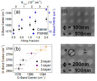
Graphene flakes used in these experiments were prepared by micromechanical exfoliation of natural graphite onto a degenerately doped p Si wafer with a thermally grown 90 nm SiO2 dielectric. Layer metrology was subsequently performed using confocal -Raman spectrometry in order to identify mono, bi, and tri-layer graphene flakes Begliarbekov et al. (2010a); Ferrari et al. (2006). Following the initial characterization, various antidot superlattices were etched onto the flakes using electron beam lithography. Figure 1c shows two exemplary lattices with different filling fractions of antidots, where is the antidot diameter, and is their separation. In accordance with previous experimental results Yan et al. (2007); Heydrich et al. (2010); Pisana et al. (2007), the corresponding Raman spectra display an energetic shift and linewidth narrowing of the G-band with increasing filling fraction, as shown in Fig 1a. The G band, which occurs at ~1580 cm-1 arises from doubly degenerate iTO and iLO phonon modes which possess symmetry. The observed stiffening (from 16.7 cm-1 to 6.6 cm-1) can be understood in terms of the Landau damping of the phonon mode, while the energetic shift arises from a renormalization of the phonon energy Yan et al. (2007); Ferrari (2007). Furthermore, the energetic shift of the G-band is positively correlated with the shift of the G’-band, as shown in Fig. 1b, which is indicative of an effective p-doping of the underlying graphene layerDas et al. (2008); Stampfer et al. (2007). In contrast, a negative correlation in the energetic shifts of the G and G’ bands would imply n-doping.
In order to correlate shift and stiffening of the G-band in antidot superlattices to an underlying carrier density, we fabricated electrically contacted devices without an antidot lattice, as shown schematically in Fig. 2b. Using the electrical field effect of the back gate, the sheet carrier density was modulated and the stiffening and energetic shift of the G-band in the unpatterned samples was used to estimate the edge state density in the antidot superlattice (see supporting online material). From these data the amount of p-doping in the antidot samples was determined to reach up to cm-2 at a filling fraction of two (top axis in Fig.1a), and was not found to depend on the number of graphene layers as shown in Fig. 1b. The large amount of effective p-doping is rather remarkable since neither extrinsic dopants, nor an external gate potential were applied to the antidot samples.
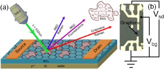
Furthermore, in order to investigate the microscopic origin of the observed p-doping we fabricated graphene-dye hybrids. Both, antidot flakes and electrically contacted devices were soaked in a 15 nanomol solution of Rhodamine 6G (R6G), as shown schematically in Fig. 2a. In these experiments, the R6G Raman peaks, the R6G fluorescence, and the Raman signal from graphene were monitored as a function of the antidot filling fraction as well as different backgate and source-drain biases on the unpatterned flakes. In the subsequent discussion, we first focus on the R6G fluorescence signal.
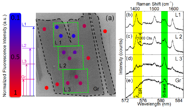
Figure 3a shows a scanning electron micrograph of a single bilayer graphene flake with three distinct antidot superlattices L1, L2, and L3, which was used to study the spatially resolved -fluorescence of the R6G dye. The relative intensity of the broad fluorescence signal of the R6G molecule (recorded at nm) normalized to the intensity of R6G fluorescence on the bare SiO2 substrate are identified by circles in Fig. 3a. Our results indicate that the R6G fluorescence is moderately quenched on the unpatterned graphene substrate as compared to the fluorescence on the bare SiO2 wafer. Remarkably, the fluorescence becomes even stronger quenched in the region were the antidot superlattices are located. The amount of R6G fluorescence quenching increases with increasing filling fraction of the antidots as shown in Figures 3b-3e for filling fractions of zero (graphene), 1/3 (L3), 1/2 (L2), and 1 (L1). The integrated intensity of the R6G fluorescence signal quenches up to a factor of five for the largest realized filling fraction, as shown in Fig 4.
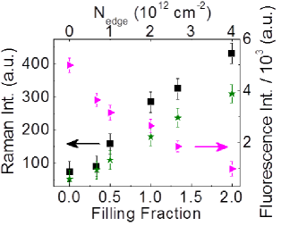
In contrast to the quenching fluorescence signal, the intensity of the Raman signals from both R6G and graphene were found to increase six-fold with increasing filling fraction, i.e. increasing density of edge states, as shown in Fig. 4. In order to rule out any possible influence of the carboxylic bonds at the edges of the antidots and the possible presence of oxygen groups on SiO2, which could have been introduced during oxygen plasma etching, a control experiment was performed in which several antidot lattices were reduced using 1 mmol L-ascorbic acid for 24 hours. Reduction in ascorbic acid was previously shown to effectively remove oxygen groups from graphene Zhang et al. (2010); Krauss et al. (2010). Our results (which are shown in the supporting online materials) indicate that no significant oxygen contamination occurs during the 10 s etching process, and thus cannot be used to account for the observed enhancement of the Raman peaks.
Phenomenologically, the fluorescence quenching may be understood as follows. The incident laser light creates electron-hole pairs in the R6G dye. In the absence of the graphene substrate, the e-h pairs radiatively recombine thereby giving rise to the fluorescence signal on the bare SiO2 wafer. It was previously shown that placing quantum dots on top of graphene results in an energy transfer from the dots into the underlying graphene layer Chen et al. (2010b), resulting in a suppression of blinking from the quantum dots. A similar effect is expected to occur for the R6G molecules on graphene, where the radiative recombination of the excitons in the R6G molecule is suppressed. In our experiments, additional quenching of the fluorescence signal in the antidot regions was observed (as shown in Figs. 3 and 4). The additional quenching can thus be understood to arise from the extra states at the edges , that effectively prevent radiative recombination of the electron-hole pairs, and therefore quench the fluorescence signal. The amount of quenching observed in our experiments is rather remarkable since increasing the antidot filling fraction decreases graphene’s surface area and introduces larger areas of SiO2 into the excitation volume on which the fluorescence is not quenched.
The observed linear increase in carrier density with increasing filling fraction is in accordance with the theoretical prediction of Whimmer et al. Wimmer et al. (2010), who showed that the ratio of edge states to bulk states is given by , where is the reduced Planck’s constant, is the Fermi velocity in graphene, is a parameter that characterizes edge roughness, is the energy width of the band of edge states, is the antidot separation, and is the antidot radius. Therefore, decreasing or alternatively increasing gives rise to a linear increase in .
I.2 Gate-Tunable Fluorescence
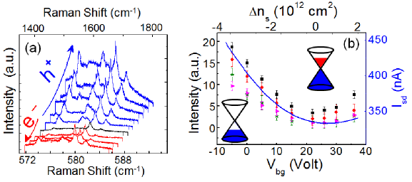
In order to further elucidate the mechanism for fluorescence quenching and the nature of we fabricated electrically contacted and back-gated graphene flakes, which did not contain an antidot superlattice. Varrying the backgate voltage, effectively moves the Fermi level in the device thereby affording the possibility of in-situ electron and hole doping of the graphene flake according to , where is the gate capacitance, is the applied gate voltage, is the location of the Dirac point, and is the electron charge Stander et al. (2009); Begliarbekov et al. (2010b); Tan et al. (2007); Bolotin et al. (2008). Modulating the Fermi level with the backgate creates a free sheet carrier density in the underlying graphene layer. The effect of free carriers on the R6G fluorescence and the R6G and graphene Raman is shown in Fig. 5a, with the blue (red) traces corresponding to spectra from hole (electron) doped regions and the black trace was taken at the Dirac point. The intensities of several Graphene and R6G Raman peaks are plotted in Fig. 5b together with the trace (blue line), which illustrates that the current to the left of the minimum (the Dirac point) is due to hole conductivity, while the current to the right of the minimum corresponds to electron conductivity. As can be seen, the intensities of both the Raman peaks as well as the fluorescence signal can be either quenched or enhanced by the applied gate bias, and directly follow the free carrier density in the device. Comparing the values of (top axis in Fig. 5b) to (top axis in Fig. 4) it is evident that the enhancement of the Raman peaks achieved in antidot devices occurs at comparable concentrations of and sheet carrier densities in unpatterned samples, as shown in Figs. 6a and 6b. Unlike the Raman peaks, the R6G fluorescence is strongly quenched in the nanopatterned samples, whereas it is enhanced in the electrically gated samples. The contrasting behavior of the fluorescence signal is strongly indicative of the different nature of the carriers in the antidot superlattice as compared to unpatterned graphene, and can be used to establish a microscopic mechanism for the observed fluorescence quenching and p-doping in the nanostructured samples.
In principle, two possible mechanisms could be responsible for fluorescence quenching: charge transfer from R6G into the trap states that are created by the additional edge state density or electrical field dissociation of the radiative R6G exciton, which leads to a strong decrease in the exciton recombination rate due to the reduced electron-hole wavefunction overlap in an electric field. Although charge transfer into trap states could account for the decrease of the fluorescence intensity, it cannot explain the observed stiffening and the energetic shift of the G-band phonon in graphene, both of which require an electric field effect Pisana et al. (2007); Yan et al. (2007). In contrast, the field dissociation mechanism explains both phenomena, as well as the absence of fluorescence quenching in unpatterned graphene under back-gate sweeping.
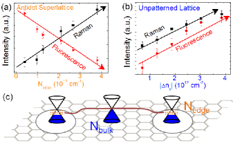
Since the edge states create spatially localized carriers, which are immobile, they would not cause the G-band stiffening. However, their presence effectively pins the Fermi level at the edges, thereby bending the band structure throughout the entire antidot superlattice, since no localized states exist in graphene’s basal plane and the Fermi level must remain continuous, as shown schematically in Fig. 6c. This band bending creates an effective potential, i.e. a built-in lateral electrical field, that accounts for the dissociation of the R6G excitons, resulting in the observed fluorescence quenching. In contrast, the vertical back-gate field of the unpatterned graphene device does not lead to band bending, while the created free carrier density can effectively feed the carrier capture into the R6G molecules, causing the observed fluorescence enhancement. The Raman signals are enhanced by the electrical field mechanism providing free carriers in both cases.
Quantitatively, the effect of the built-in electrical field may be estimated to first order from the amount of p-doping that it introduces. In graphene, doping is commensurate with the movement of the Fermi level into the conduction or valence bands by the electrical field. The band offset as a function of doping concentration is given by , where is the reduced Planck’s constant, is the Fermi velocity, and is the Fermi wave vector, which in graphene is given by Hwang et al. (2007). The antidot lattices used in our experiments yielded doping concentrations on the order of cm-2, which correspond to band offsets of meV.
The Fermi level pinning at the localized carrier density in the antidot superlattice is similar to Fermi level pinning of a Schottky barrier at an graphene-metal interface that is used to separate photogenerated carriers in optoelectronic devices based, for example, on carbon nanotubes Avouris (2006); Mueller et al. (2009); Xia et al. (2009). In our case, however, no metal was deposited onto graphene and the pinning occurs at the localized edge states that are a direct consequence of the antidot superlattice.
In summary, we fabricated several graphene antidot superlattices using mono, bi, and tri layer flakes, and observed effective p-type doping which increases with larger filling fractions, as evident from their Raman signatures. We furthermore showed that after depositing R6G dye on these flakes, the corresponding fluorescence signal is strongly quenched with increasing antidot filling fraction, while the Raman signal is enhanced. These results are indicative to a microscopic mechanism in which the Fermi level becomes pinned at the antidot periphery giving rise to a built-in electric field, which accounts for the fluorescence quenching and the observed p-type doping in nanopatterned graphene. These findings make antidot lattices of great interest for carbon-based optoelectronics and might be particularly useful for light-harvesting applications such as photodetectors and solar cells requiring efficient field separation of electron-hole pairs.
References
- Novoselov et al. (2004) K. S. Novoselov, A. K. Geim, S. V. Morozov, D. Jiang, Y. Zhang, S. V. Dubonos, I. V. Grigorieva, and A. A. Firsov, Science 306, 666 (2004).
- Lin et al. (2010) Y. M. Lin, C. Dimitrakopoulos, K. A. Jenkins, D. B. Farmer, H. Y. Chiu, A. Grill, and P. Avouris, Science 327, 662 (2010).
- Bolotin et al. (2008) K. I. Bolotin, K. J. Sikes, Z. Jiang, M. Klima, G. Fudenberg, J. Hone, P. Kim, and H. L. Stormer, Solid State Communications 146, 351 (2008).
- Balandin et al. (2008) A. Balandin, W. Z. G. S. Bao, I. Calizo, D. TeweldebrhanD, F. Miao, and C. N. Lau, Nano Letters 8, 902 (2008).
- Lee et al. (2008) C. Lee, X. Wei, J. W. Kysar, and J. Hone, Science 321, 385 (2008).
- Bonaccorso et al. (2010) F. Bonaccorso, Z. Sun, T. Hasan, and A. C. Ferrari, Nature Photonics 4, 611 (2010).
- Novoselov et al. (2007) K. S. Novoselov, S. V. Morozov, T. M. G. Mohinddin, L. A. Ponomarenko, D. C. Elias, R. Yang, I. I. Barbolina, P. Blake, T. J. Booth, D. Jiang, et al., Physica Status Solidi B-basic Solid State Physics 244, 4106 (2007).
- Neto et al. (2009) A. C. Neto, F. Guinea, N. Peres, K. Novoselov, and A. Geim, Rev. Mod. Phys 81, 109 (2009).
- Xia et al. (2009) F. Xia, T. Mueller, Y. ming Lin, A. Valdes-Garcia, and P. Avouris, Nature Nanotechnology 4, 839 (2009).
- Nair et al. (2008) R. R. Nair, P. Blake, A. N. Grigorenko, K. S. Novoselov, T. J. Booth, T. Stauber, N. M. R. Peres, and A. K. Geim, Science 320, 5881 (2008).
- Gierz et al. (2007) I. Gierz, C. Riedl, U. Starke, C. R. Ast, and K. Kern, Nano Letters 8, 4603 (2007).
- Wang et al. (2010) Y. Wang, Y. Shao, D. W. Matson, J. Li, and Y. Lin, ACS Nano 4, 1790 (2010).
- Wehling et al. (2008) T. O. Wehling, K. S. Novoselov, S. V. Morozov, E. E. Vdovin, M. I. Katsnelson, A. K. Geim, and A. I. Lichtenstein, Nano Letters 8, 173 (2008).
- Dong et al. (2009) X. Dong, D. Fu, W. Fang, Y. Shi, P. Chen, and L.-J. Li, Small 5, 1422 (2009).
- Guo et al. (2010) B. Guo, Q. Liu, E. Chen, H. Zhu, L. Fang, and J. R. Gong, Nano Letters In Press (2010).
- Mueller et al. (2009) T. Mueller, F. Xia, M. Freitag, J. Tsang, and P. Avouris, Phys. Rev. B 79, 245430 (2009).
- Mueller et al. (2010) T. Mueller, F. Xia, and P. Avouris, Nature Photonics 4, 297 (2010).
- Avouris (2006) P. Avouris, Materials Today 9, 46 (2006).
- Hong et al. (2010) G. Hong, S. M. Tabakman, K. Welsher, H. Wang, X. Wang, and H. Dai, J. Am. Chem. Soc. 132, 15920 (2010).
- Chen et al. (2010a) Z. Chen, S. Berciaud, C. Nuckolls, T. F. Heinz, and L. E. Brus, ACS Nano 4, 2964 (2010a).
- Wimmer et al. (2010) M. Wimmer, A. R. Akhmerov, and F. Guinea, Phys. Rev. B 82, 045409 (2010).
- Bai et al. (2010) J. Bai, X. Zhong, S. Jiang, Y. Huang, and X. Duan, Nature Nanotechnol. 5, 190 (2010).
- Liang et al. (2010) X. Liang, Y.-S. Jung, S. Wu, A. Ismach, D. L. Olynick, S. Cabrini, and J. Bokor, Nano Lett. 10, 2454 (2010).
- Kim et al. (2010) M. Kim, N. S. Safron, E. Han, M. S. Arnold, and P. Gopalan, Nano Lett. 10, 1125 (2010).
- Sinitskii and Tour (2010) A. Sinitskii and J. M. Tour, J. Am. Chem. Soc. 132, 14730 (2010).
- Stojanovic et al. (2010) V. M. Stojanovic, N. Vukmirovic, and C. Bruder, Phys. Rev. B 82, 165410 (2010).
- Petersen and Pedersen (2009) R. Petersen and T. G. Pedersen, Phys. Rev. B 80, 113404 (2009).
- Heydrich et al. (2010) S. Heydrich, M. Hirmer, C. Preis, T. Korn, J. Eroms, D. Weiss, and C. Schuller, Appl. Phys. Lett. 97, 043113 (2010).
- Begliarbekov et al. (2010a) M. Begliarbekov, O. Sul, S. Kalliakos, E.-H. Yang, and S. Strauf, Appl. Phys. Lett. 97, 031908 (2010a).
- Ferrari et al. (2006) A. C. Ferrari, J. C. Meyer, V. Scardaci, C. Casiraghi, M. Lazzeri, F. Mauri, S. Piscanec, D. Jiang, K. S. N. S., Roth, et al., Phys. Rev. Lett 97, 187401 (2006).
- Yan et al. (2007) J. Yan, Y. Zhang, P. Kim, and A. Pinczuk, Phys. Rev. Lett 98, 166802 (2007).
- Pisana et al. (2007) S. Pisana, M. Lazzeri, C. Casiraghi, K. S. Novoselov, A. K. Geim, A. C. Ferrari, and F. Mauri, Nature Materials 6, 198 (2007).
- Ferrari (2007) A. C. Ferrari, Solid State Communications 143, 47 (2007).
- Das et al. (2008) A. Das, S. Pisana, B. Chakraborty, S. Piscanec, S. K. Saha, U. V. Waghmare, K. S. Novoselov, H. R. Krishnamurthy, A. K. Geim, A. C. Ferrari, et al., Nature Nanotechnology 3, 210 (2008).
- Stampfer et al. (2007) C. Stampfer, F. Molitor, D. Graf, K. Ensslin, A. Jungen, C. Hierold, and L. Wirtz, Appl. Phys. Lett. 91, 241907 (2007).
- Zhang et al. (2010) J. Zhang, H. Yang, G. Shen, P. Cheng, J. Zhang, and S. Guo, Chem. Commun. 46, 1112 (2010).
- Krauss et al. (2010) B. Krauss, P. Nemes-Incze, V. Skakalova, L. P. Biro, K. von Klitzing, and J. H. Smet, Nano Lett. 10, 4544 (2010).
- Chen et al. (2010b) Z. Chen, S. Berciaud, C. Nuckolls, T. F. Heinz, and L. E. Brus, ACS Nano 4, 2964 (2010b).
- Stander et al. (2009) N. Stander, B. Huard, and D. Goldhaber-Gordon, Phys. Rev. Lett. 102, 026807 (2009).
- Begliarbekov et al. (2010b) M. Begliarbekov, O. Sul, N. Ai, E.-H. Yang, and S. Strauf, Appl. Phys. Lett. 97, 122106 (2010b).
- Tan et al. (2007) Y.-W. Tan, Y. Zhang, K. Bolotin, Y. Zhao, S. Adam, E. H. Hwang, S. D. Sarma, H. L. Stormer, and P. Kim, Phys. Rev. Lett. 99, 246803 (2007).
- Hwang et al. (2007) E. Hwang, S. Adam, and S. D. Sarma, Phys. Rev. Lett. 98, 186806 (2007).