Radiation hardness of CMS pixel barrel modules
Abstract
Pixel detectors are used in the innermost part of the multi purpose experiments at LHC and are therefore exposed to the highest fluences of ionising radiation, which in this part of the detectors consists mainly of charged pions. The radiation hardness of all detector components has thoroughly been tested up to the fluences expected at the LHC. In case of an LHC upgrade, the fluence will be much higher and it is not yet clear how long the present pixel modules will stay operative in such a harsh environment. The aim of this study was to establish such a limit as a benchmark for other possible detector concepts considered for the upgrade.
As the sensors and the readout chip are the parts most sensitive to radiation damage, samples consisting of a small pixel sensor bump-bonded to a CMS-readout chip (PSI46V2.1) have been irradiated with positive 200 MeV pions at PSI up to and with 21 GeV protons at CERN up to .
After irradiation the response of the system to beta particles from a 90Sr source was measured to characterise the charge collection efficiency of the sensor. Radiation induced changes in the readout chip were also measured. The results show that the present pixel modules can be expected to be still operational after a fluence of . Samples irradiated up to still see the beta particles. However, further tests are needed to confirm whether a stable operation with high particle detection efficiency is possible after such a high fluence.
keywords:
LHC , super LHC , CMS , tracking , pixel , silicon , radiation hardnessPACS:
07.89 , 29.40.Gx , 29.40.Wk , 61.80.-x1 Introduction
Hybrid silicon pixel detectors are used in the innermost part of the multi purpose experiments at LHC at distances between 4 and 12 cm from the beam [1, 2]. They are therefore exposed to the highest fluences of ionising radiation, which in this part of the detectors consists mainly of charged pions. The radiation hardness of all detector components has thoroughly been tested up to the fluences expected at the LHC [3]. A replacement of the present CMS pixel detector by an improved 4-layer system is already planned for 2014 [4]. As a two stage luminosity upgrade of the LHC is foreseen shortly after [5], it has to be assured that the new system is suitable for peak luminosities above cm-2s-1 in terms of radiation hardness and data transfer. The short time scale allows only for very limited R&D and it has to be tested if the present detector concept can be adjusted to the new specifications. This paper reports on the radiation hardness of both the sensor and the readout chip, with the aim to estimate their fluence limits and their lifetime in an upgraded LHC.
2 CMS Modules
The pixel detector of CMS is a so called hybrid pixel detector. This means that the sensor part, which actually detects the charged particles, and the readout electronics are on separate substrates. Each sensing element (pixel) is connected to its preamplifier located on the readout chip by a small indium bowl, the so-called bump. The power and I/O pads of the readout chip are then wire bonded to a high density interconnect (HDI) which provides the connection to the outside.
The two parts most sensitive to radiation damage are the sensor and the readout chip. Therefore this study is limited to those components. In order to further simplify the irradiation procedure only small modules consisting of one ROC and a small sensor covering the area of this ROC were used. Such samples are about cm2 large which is about the beam spot size in the irradiation sites chosen. So, scanning during irradiation could be avoided. However, in contrast to strip detectors, where the strip length is important, small pixel devices contain all relevant features of a full module and the results obtained in this study are fully valid.
2.1 The Sensor
The sensors for the CMS pixel barrel are made of silicon and follow the so called “n-in-n” approach. The collection of electrons is advantageous because of their higher mobility compared to holes. It causes a larger Lorentz drift of the signal charges which leads to charge sharing between between neighboring pixels and so improves the spatial resolution. Further the higher mobility of electrons makes them less prone to trapping, which is essential after high fluences of charged particles. After irradiation induced space charge sign inversion, the highest electric field in the sensor is located close to the n-electrodes used to collect the charge, which is also of advantage.
The choice of n-substrate requires a double sided sensor process, meaning that both sides of the sensor need photolithographic steps. This leads to higher costs compared to single sided p-in-n (or n-in-p) sensors. However, the double sided sensors have a guard ring scheme where all sensor edges are at a ground potential and this greatly simplified the design of detector modules. The n-side isolation was implemented through the so-called moderated p-spray technique [6] with a punch through biasing grid.
The sensor samples were taken from wafers of the main production run for the CMS pixel barrel which were processed on approximately m thick n-doped DOFZ silicon according to the recommendation of the ROSE-collaboration [7]. The resistance of the material prior to irradiation was leading to an initial full depletion voltage of V.
2.2 The Readout Chip
The CMS pixel readout chip (called PSI46V2.1) described in detail in [8] has been fabricated in a commercial five-metal layer m process available via CERN. The chip contains about 1.3 million transistors on an area of mm2. It is divided into three functional blocks: the array of pixel unit cells of m2 size organised in 26 double columns, the double column perifery, and a control and a chip perifery containing a supply and control block.
The radiation hardness of the m technology is well known if certain layout recommendations are followed [9]. This concerns the leakage currents, which are strongly surpressed by a “closed gate” geometry of the NMOS transistors and channel stop rings. The shift of the transistor thresholds is small due to the small thickness of the gate oxides in such processes. Other radiation induced effects like the reduction of the surface mobility and the minority carrier life time remain. The former might effect the transconductance of the transistors and by this the speed of the chip while the latter influences the bipolar devices like diodes.
3 Sample Preparation
The readout chips taken are identical to those used for building the CMS pixel detector. The small sensors were produced on the same wafers as those for full modules and identical to those apart from the size. Both parts were joined using the bump bonding process used for the module production for the CMS pixel barrel [10]. As this procedure includes processing steps at temperatures above C, it was done before irradiation. This means that the sensors and readout chips had to be irradiated at the same time. This way, a realistic picture of the situation in CMS after a few years of running could be obtained.
The sandwiches of sensor and readout chip were irradiated at the PSI-PiE1-beam line [11] with positive pions of momentum 200 MeV/c to fluences up to and with 26 GeV/c protons at CERN-PS [12] up to .
All irradiated samples were kept in a commercial freezer at C after irradiation. However, the pion irradiated ones were accidentally warmed up to room temperature for a period of a few weeks.
4 Sensor Performance
The aim of this study was to determine the signal obtained from minimum ionizing particles (m.i.p.) which is the limiting factor for the use of such type of sensors.
4.1 Measurement Procedure
For reasons of simplicity, a 90Sr source has been used for inducing the signal in the sensor. The -spectrum of the daughter decay of 90Y has an endpoint energy of about 2.3 MeV and therefore contains particles which approximate a m.i.p. well. However, there are also a lot of low energy particles which lead to an energy deposition in the sensor which is much higher.
The samples were mounted on a pair of water cooled Peltier elements and kept below C. The source was placed inside the box a few millimetres above the sample. For acquiring the data a so-called random trigger was used. In this mode of operation an arbitrary cycle of the clock is stretched by a large factor, and a trigger is sent in a way that all the hits within this clock cycle are read out. The stretch factor was a adjusted such that about 80 % of the triggers showed hits. As this method does not allow for hit detection efficiency measurements, the upgrade of the setup with an independent scintillator trigger is currently underway.
The testing and calibration procedure was similar to what is used for the qualification of CMS pixel barrel modules [13]. The threshold to which the pixels were adjusted was e- for all samples up to a fluence of . For the higher fluence the threshold was lowered to a value between and e-. After, calibration data was taken using the 90Sr source. The sensor bias was varied from 50 V up to 1100 V for some of the most irradiated samples. The temperature was kept stable within C during the bias scan.
The data was analysed offline. First, all analog signals were converted into an absolute charge value [14]. Then a mask was generated to exclude noisy and unbonded pixels from further analysis. Finally, all clusters not contiguous with a masked pixel were reconstructed. The charge of the clusters was histogrammed separately for each cluster size. The spectra were fit to a Landau function convoluted with a Gaussian. The charge value quoted is the most probable value (MPV) from this fit.
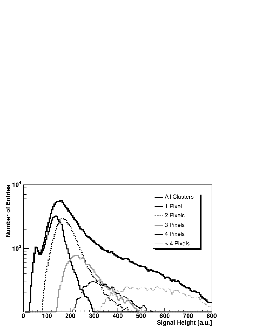
The radiation of the 90Sr source contains a sizable fraction of low energy electrons which might be stopped in the sensor and cause a much higher signal than a minimum ionising particle. A part of the secondary electrons, however, travels in parallel to the sensor surface resulting in large clusters. Figure 1 shows the pulse height spectrum of a sample irradiated to at a bias voltage of 800 V for different cluster sizes. The large fraction of 2-clusters and the occurrence of clusters larger than 2 pixels cannot be explained by simple charge sharing and clearly indicated the presence of low energy electrons from the source. The same is the case for the strong dependence of the MPV on the cluster size. In order not to bias the data only the spectra of single hit clusters have been used.
4.2 Results
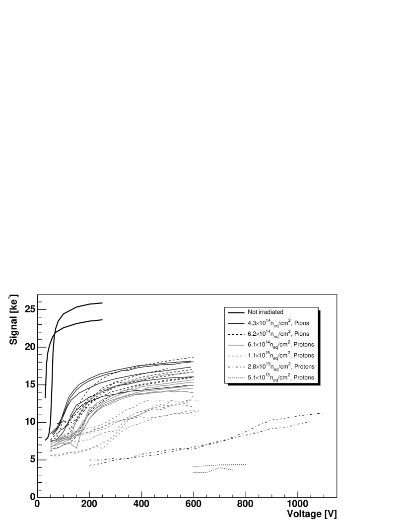
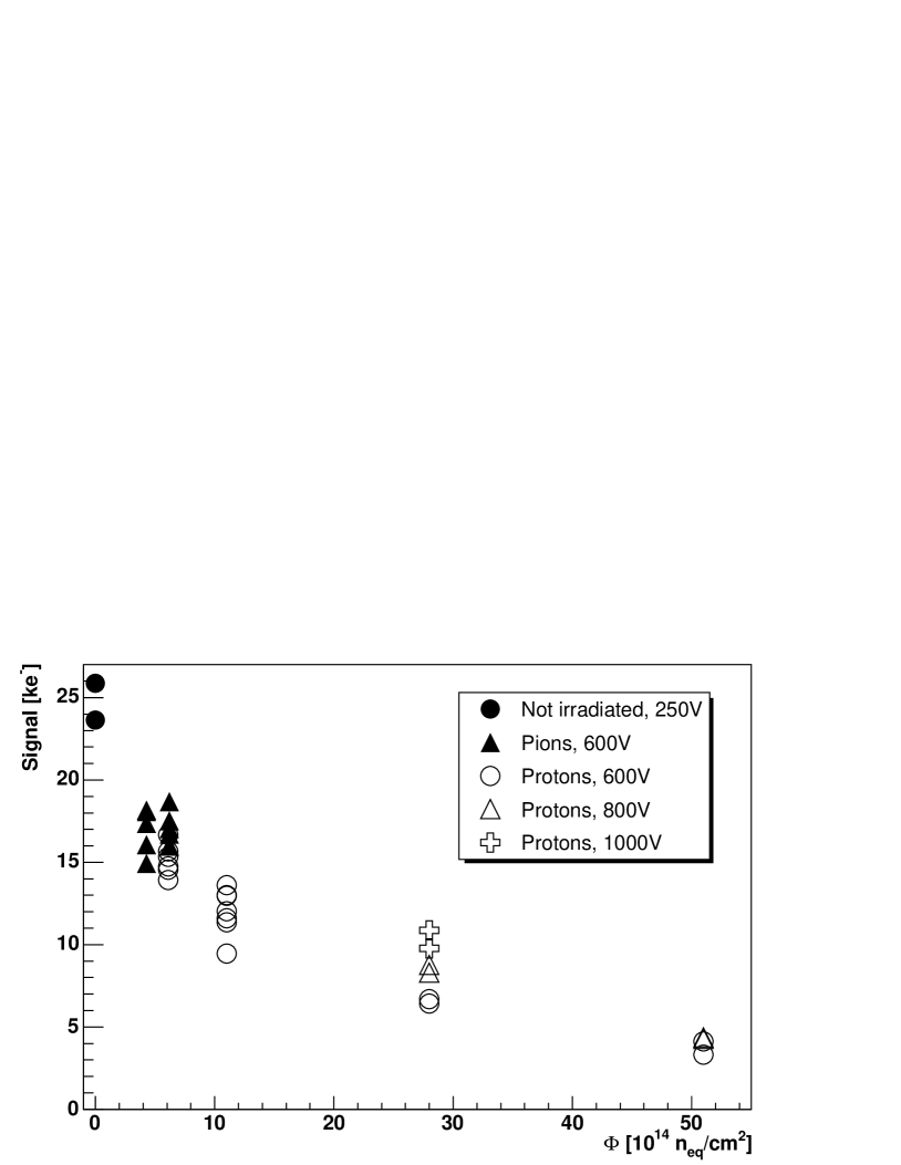
Figure 2 shows the values of the MPV for all the measured samples and all biases. For the unirradiated samples the steep rise of the signal at the full depletion voltage of V is visible. The signal plateau is reached very fast.
The samples irradiated to fluences in the -range also show a saturation of the signal above roughly 300 V. However, the variation of the saturated signal for the same irradiation fluence is of the same order of magnitude as the reduction of the signal from to . A distinction of the irradiation fluence of the samples from the height of the plateau is not possible. This strong variation cannot be explained by differences in the sensor thickness and is probably caused by the imperfection of the pulse height calibration. It relies on the assumption that the injection mechanism for test pulses is equal for all readout chips, which is not the case. Variations of the injection capacitor are larger than .
The differences in the irradiation fluence are better reflected in the “low” voltage part of the curves, where the voltage from which the signal starts to rise reflects the radiation-induced increase of the space charge.
For the samples irradiated to fluences above , no saturation of the signal with increasing bias is visible. It is remarkable that even after a fluence of a charge of more than 10 000 electrons can be collected if a bias voltage over 800 V is applied.
The samples irradiated to , can clearly detect the particles. However, the signal obtained is well below 5000 electrons which is too little for reliable operation as a tracking device. The data were taken at a temperature of about C and therefore the leakage current was above A for the about cm2 large device. This did not allow measurements above 800 V.
To display the development of the signal height as a function of the fluence, the charge at 600 V was measured for each sample (250 V for the unirradiated ones) and plotted in Fig. 3. In addition, values for 800 V and 1000 V are shown for the highest fluence. Apart from the large fluctuations the reduction of the charge with fluence is visible. Further it becomes obvious that it pays to go to very high bias voltages if the fluences exceed .
The charge values in this study are lower than those reported elsewhere [15, 16]. The authors in these studies suggested that some kind of avalanche multiplication was the reason for the higher than expected signals. The sensors used in this study are designed differently. The layout of the pixel’s n+-implants was optimized to avoid peaks of the electric field. Therefore the IV-curves of the sensors tested do not show evidence for an onset of micro discharge.
5 Performance of the Readout Chip
In general it can be stated that all of the ROCs, even at the highest fluence, worked well and could be operated using the standard calibration software. For the ROC with a fluence above the feedback circuit of the preamplifier and shaper had to be adjusted, and the sampling point of the ADC, reading the chip data had to be shifted for a few nanoseconds.
The parameters of the readout chip which are subject to change due to irradiation are not directly accessible in the readout chips. For an extraction of the transistor parameters a special test chip would be necessary. However, there are some chip parameters which give, indirectly, hints on the radiation induced changes in the ROC.
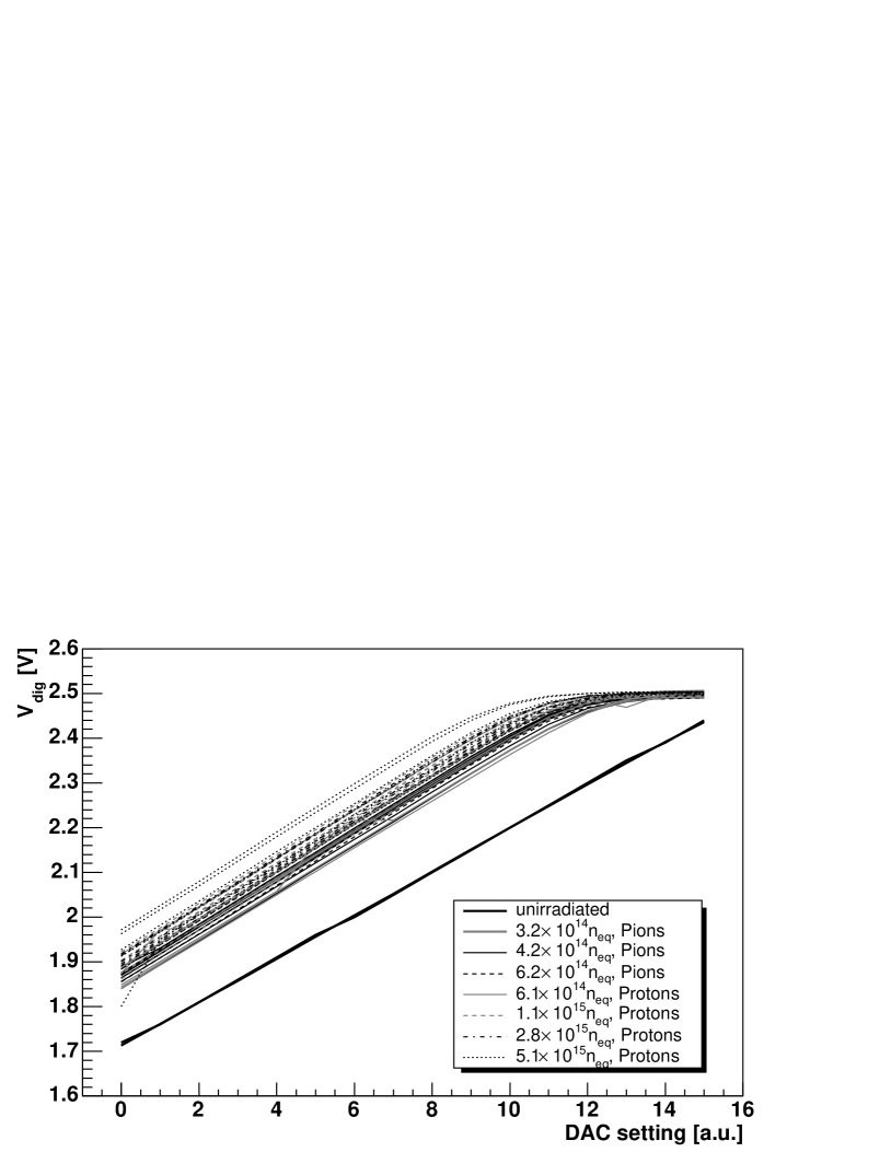
One very sensitive block in the periphery is the band gap reference which is used as a reference for all internal voltages set. One of theses voltages is stabilized using an external SMD-capacitor and can therefore be measured using a probe. The band gap reference is in principle a forward biased diode whose reference voltage might be dependent on the minority carrier life time. Measuring the digital voltage as a function of the adjusted DAC setting is therefore a test of the stability of the band gap reference. The result of this measurement is shown in Fig. 4. The output of the band gap reference shows a shift of about 10 % already at the lowest fluence and then stays constant. This is a hint of a surface effect which usually saturates at low doses. The saturation of the voltage at DAC values above 10 is due to the fact the supply voltage of 2.5 V cannot be exceeded.
Another parameter, which might be prone to radiation induced changes, is the rise time of the preamplifier. This causes the so called time walk and either needs to be compensated by an increase of the analog current or results in a higher in-time threshold.
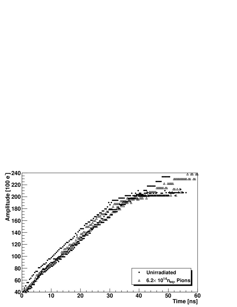
The pulse shape of the PSI46V2.1 cannot be measured directly, but an indirect method gives a hint on its leading edge. It is based on calibration pulses which can be injected into each pixel. With a certain DAC setting, called calibration delay, the time of this pulse can be shifted with respect to the leading edge of the clock cycle whose signals will be read out. If this DAC is scanned while the height of the calibration signal and the threshold stays constant, an efficiency curve will be obtained. If the pulse is injected too early it will cross the threshold in the clock cycle before the readout and will not be seen. If it is too late it will be assigned to the next clock cycle. The plateau of full efficiency in-between the two regions is exactly one clock cycle wide i.e. 25 ns. If this scan is repeated with a lower threshold and the same calibration pulse height, the efficiency plateau will be slightly shifted due to the fact that the threshold will be reached slightly earlier. If the whole space of the threshold and the calibration delay is scanned, the timing of the leading edge of the pulse shape can be reconstructed.
The result of such a reconstruction is shown in fig. 5 for one pixel each in three unirradiated ROCs and two ROCs irradiated to . The analog current was the same in all the measurements. The rise time of the pulse is about 35 ns and, most remarkable, it does not change with irradiation, at least not up to the level investigated.
6 Conclusion
Sandwiches of a CMS pixel readout chip and a small single chip sensor have been irradiated up to flucences of . Test with a 90Sr source showed a signal above 10 000 electrons per m.i.p. can be achived at bias voltage of or below 600 V up to a fluence of about . The samples irradiated up to , however, needed a bias voltage of 1000 V to reach a signal of 10 000 electrons. This indicates the suitabiliy of these devices for an upgraded LHC up to rather small radii. The samples which obtained a fluence of could only be measured up to a bias voltage of 800 V due to limitations of the cooling. They still showed signals, but their amplitude seems too low for an eficient tracking. Measurements at higher bias voltages are a subject of further studies, as well as efficiency measurements using an independent scintillator trigger.
The readout chip performed well even after the highest fluence. It could be operated with the standard calibration method and only very few settings, like the feedback resistor of the preamplifier and shaper, needed to be adjusted. A degradation of the amplifier’s rise time could not be detected by this study. The band gap reference of the chip drifted by about 10 % already after lowest fluence, but this shift saturated. Further studies to characterize the irradiated readout chips are under way.
Acknowledgement
The pion irradiation at PSI would not have been possible without the beam line support by D. Renker and K. Deiters, PSI, the logistics provided by M. Glaser, CERN, and the great effort of C. Betancourt and M. Gerling, UC Santa Cruz (both were supported by a financial contribution of RD50 and PSI).
The proton irradiation was carried out at the CERN irradiation facility. The authors would like to thank M. Glaser and the CERN team for the outstanding service.
Thanks are also due to N. Krzyzanowski and E. Stachura, UIC for the measurements of the irradiated ROCs.
The work of A. Bean and V. Radicci is supported by the PIRE grant OISE-0730173 of the US-NSF.
The sensors were produced by CiS GmbH in Erfurt, Germany.
References
- [1] The CMS Collaboration, The CMS experiment at the CERN LHC, Journal of Instrumentation 3 S08004 (2008) 26–89, http://www.iop.org/EJ/journal/-page=extra.lhc/jinst.
- [2] The ATLAS Collaboration, The ATLAS experiment at the CERN large hadron collider, Journal of Instrumentation 3 S08003 (2008) ??, http://www.iop.org/EJ/journal/-page=extra.lhc/jinst.
- [3] Y. Allkofer, et al., Design and performance of the silicon sensors for the cms barrel pixel detector, Nucl. Instrum. Methods A 584 (2008) 25 – 41.
- [4] A. Bean, et al., The CMS pixel detector and challenges (prospectives) for its upgrade, these proceedings.
- [5] EP-TH faculty meeting, CERN, 17.01.2001.
- [6] J. Kemmer, et al., Streifendetektor, Patentoffenlegungsschrift DE 19620081 A1.
- [7] G. Lindström, et al., Radiation hard silicon detectors – developments by the RD48 (ROSE) collaboration, Nucl. Instrum. Methods A 466 (2001) 308–326.
- [8] H.-C. Kästli, et al., Design and performance of the CMS pixel detector readout chip, Nucl. Instrum. Methods A 565 (2006) 188–194.
- [9] W. Snoeys, et al., Layout techniques to enhance the radiation tolerance of standard CMOS technologies demonstrated on a pixel detector readout chip, Nucl. Instrum. Methods A 439 (2000) 349–360.
- [10] C. Brönnimann, et al., Development of an indium bump bond process for silicon pixel detectors at PSI, Nucl. Instrum. Methods A 565 (2006) 303–308.
- [11] F. Foroughi, et al., http://aea.web.psi.ch/beam2lines/beam_pie1.html.
- [12] M.Glaser, et al., http://irradiation.web.cern.ch/irradiation/irrad1.htm.
- [13] L. Caminada, A. Starodumov, Building and commissioning of the CMS pixel barrel detector, presented at the Pixel 2008 international workshop, Fermilab, Batavia, IL, USA, 23.-26. September 2008, to be published in Jinst.
- [14] S. Dambach, CMS pixel module readout optimization and study of the lifetime in the semileptonic decay mode, Ph.D. thesis, ETH Zürich, Switzerland, ETH Diss. No. 18203 (2009).
- [15] A. Affolder, P. Allport, G. Casse, Title not yet known, these proceedings.
- [16] I. Mandic̀, V. Cindro, G. Kramberger, M. Mikuz̆, Observation of full charge collection efficiency in p+n strip detectors irradiated up to , presented at the RESMDD 2008 in Florence, to be published in NIM A.