NaAlSi: a self-doped semimetallic superconductor
with free electrons
and covalent holes
Abstract
The layered ternary conductor NaAlSi, possessing the iron-pnictide “111” crystal structure, superconducts at 7 K. Using density functional methods, we show that this compound is an intrinsic (self-doped) low-carrier-density semimetal with a number of unusual features. Covalent Al-Si valence bands provide the holes, and free-electron-like Al bands, which propagate in the channel between the neighboring Si layers, dip just below the Fermi level to create the electron carriers. The Fermi level (and therefore the superconducting carriers) lies in a narrow and sharp peak within a pseudogap in the density of states. The small peak arises from valence bands which are nearly of pure Si, quasi-two-dimensional, flat, and coupled to Al conduction bands. Isostructural NaAlGe, which is not superconducting above 1.6 K, has almost exactly the same band structure except for one missing piece of small Fermi surface. Certain deformation potentials induced by Si and Na displacements along the -axis are calculated and discussed. It seems likely that the mechanism of pairing is related to that of several other lightly doped two-dimensional nonmagnetic semiconductors (TiNCl, ZrNCl, HfNCl), which is not well understood but apparently not of phonon origin.
I Introduction
The discovery of new superconductors in unexpected materials brings the potential to understand something deeper, or perhaps something different, about the underlying properties that favor superconducting pairing. The discovery of high-temperature superconductivity (to 56 K so far) in Fe-pnictidesKamihara et al. (2008) is a recent spectacular example, and is also an example of close relationships between magnetism and superconductivity, though the connections are still far from clear.
New superconductors where little or no magnetic effects are present are also arising, and these clearly involve different physics from the cuprate or Fe-pnictide high-temperature superconductors. Electron-doped MNCl, where M = Zr or Hf, becomes superconducting immediately upon undergoing the insulator-to-metal transition,Yamanaka et al. (1996); Shamoto et al. (1998); Yamanaka et al. (1998); Shamoto et al. (1999) which, in the case of M = Hf, is higher than 25 K. The similarly layered, electron-doped, ionic insulator TiNCl superconducts up to 16 K. Magnetic behavior in these materials is at most subtle, amounting to an enhancement in Pauli susceptibility near the metal-to-insulator transition.Yamanaka et al. (2009)
In this paper we address the ternary silicide NaAlSi (space group P4/nmm, ), another ionic and layered material that shows unexpected superconductivity, and does so in its native (without doping or pressure) stoichiometric state, at 7 K.Kuroiwa et al. (2007) NaAlSi introduces new interest from several viewpoints. First, it is an electron superconductor, with a high for such materials at ambient pressure. Pb is an superconductor with comparable (7.2 K) but with simple metallic bonding and heavy atoms, making it very different. Doped SiBustarret et al. (2006) and doped diamondEkimov et al. (1998) superconduct in the same range, and are of course very different classes of materials. A more relevant example is the pseudo-ternary compound Ba1-xKxBiO3 (BKBO), which undergoes an insulator-to-metal transition for , beyond which its surpasses 30 K.[bkbo, ; bkbo2, ]
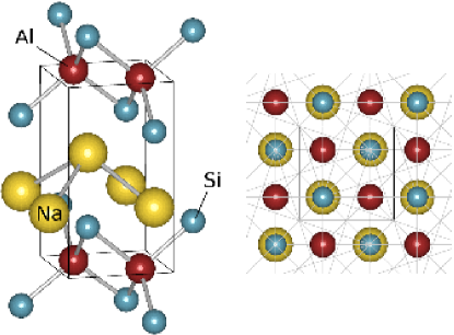
Second, the Al-Si layered substructure is like that of the FeAs layer in the Fe-pnictide superconductors, raising the possibility of some connections between their electronic structures. In fact, NaAlSi has the same structure as the Fe-pnictide “111” compounds, with Al being tetrahedrally coordinated by Si (analogous to Fe being tetrahedrally coordinated by As). In spite of their structural similarities, these compounds have major differences; for example, the Fe pnictides are electron systems with magnetism, while NaAlSi is an electron system without magnetism.
Third, NaAlSi is the isovalent sister (one row down in the periodic table for each atom) of LiBC. LiBC itself is (in a sense) isovalent and also isostructural to MgB2; however due to the B-C alternation around the hexagon in the honeycomb-structure layer, LiBC is insulating rather than conducting. When hole-doped while retaining the same structure, Li1-xBC has stronger electron-phonon coupling than does MgB2.Rosner et al. (2002) While NaAlSi has a substantially different structure than LiBC, its isovalence and its combination of covalence with some ionic character is shared with LiBC.
Yet another closely related compound is CaAlSi, whose two different stacking polymorphs and parent structure superconduct in the 5–8 K range.Sagayama et al. (2006); Kuroiwa et al. (2006) Linear-response and frozen-mode calculations indicate electron-phonon coupling is the likely mechanism; in particular, an ultra-soft phonon mode appears and is suggested to play a role in the superconductivity.Shein et al. (2003); Huang et al. (2004); Mazin and Papaconstantopoulos (2004); Giantomassi et al. (2005); Heid et al. (2007); Kuroiwa et al. (2008) It is curious that in this compound, where divalent Ca (comparing it with NaAlSi) contributes one additional electron into the Si-Al bands, the preferred structure is that of AlB2 (i.e., MgB2) with planar bondingShein et al. (2003); Huang et al. (2004); Giantomassi et al. (2005) rather than the more -like bonding in NaAlSi. Electronic structure calculations show that CaAlSi has one electron in the conduction band above a bonding-antibonding band separation at the NaAlSi band-filling level, a situation which would not appear to be particularly favorable for bonding.
In this paper we analyze first-principles electronic structure calculations that reveal that NaAlSi is a naturally self-doped semimetal, with doping occurring—thus charge transfer occurring—between covalent bands within the Al-Si substructure, and two-dimensional (2D) free-electron-like bands within the Al layer. The resulting small Fermi surfaces (FSs) are unusual, complicated by the small but seemingly important interlayer coupling along the crystalline -axis.
II Computational Methods
First-principles, local density approximation (LDA) calculations were carried out using the full-potential local-orbital (FPLO) scheme.Koepernik and Eschrig (1999) A -point mesh of was used, and the Perdew-Wang 92 approximationPerdew and Wang (1992) was applied for the exchange-correlation potential. The experimental lattice constants obtained by Kuroiwa et al.Kuroiwa et al. (2007) ( Å and Å) and internal coordinates published by Westerhaus and SchusterWesterhaus and Schuster (1979) (, ) were used in our calculations.
III Electronic Structure
III.1 Discussion of the band structure
The calculated band structure of NaAlSi is shown in Fig. 2. As expected, the Na ion gives up its electron to the Si-Al-Si trilayer (see Fig. 1), which may have some ionic character, though it is not easy to quantify (the valence bands have much more Si character than Al character, seemingly more than suggested by their number of valence electrons). There are several readily identifiable classes of bands. Two primarily Si bands, with a small amount of Al character, are centered 9 eV below the Fermi level and have a width of 2.5 eV. Above them there is a six-band complex of Al-Si - bands (heavily Si) that are very nearly filled, the band maximum only slightly overlapping .
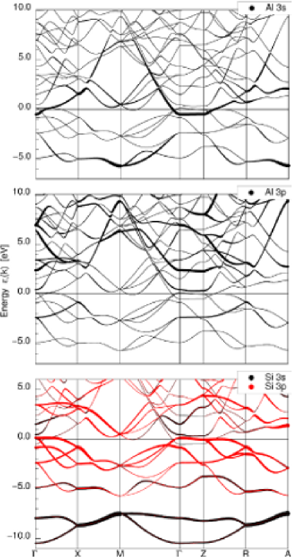
Above lie non-bonding and antibonding bands, and the Na bands. Among these there are a pair of distinctive bands, which can be identified most easily by their Al character in the top panel of Fig. 2. These bands are nearly free-electron-like with large dispersions, and cross many other bands with little mixing. Along -M they are degenerate and easily identifiable in Fig. 2, as they disperse up through the Fermi level to nearly 10 eV at the M point. Along -X, and similarly at the top of the zone Z-R, they are distinct: one again disperses upward rapidly, cutting through many other bands, also to nearly 10 eV at X; the other disperses much more weakly to X, with a bandwidth of about 2 eV. Their Al character and nearly vanishing Si character identify these as free-electron states, in which electrons move down channels of Al atoms separately in and directions. (Note that their lack of dispersion identifies them as planar bands.) There is some coupling to the states in a parallel channel of Al atoms, giving rise to the 2 eV transverse dispersion. These bands lie 0.5 eV below at and contain electrons. Without interference with other bands near the Fermi level and supposing them to be isotropic in the plane (but see below), such FSs might include 3–4% of the area of the zone, which would equate to an intrinsic electron doping for two bands, both spins of around 0.12–0.16 carriers per unit cell, and the concentration of hole carriers would be equal. The anisotropy, discussed below, makes the actual carrier concentration much lower.
The small overlap of valence and conduction bands results in semimetallic character and small Fermi surfaces. The valence bands are quite anisotropic. Looking at the valence bands along -X, one might try to characterize them as one “heavy-hole” and one “light-hole” band, degenerate at , with the band maximum lying 0.13 eV above . However, the heavy hole band is actually almost perfectly flat for the first third of the -X line, before dispersing downward across and farther below. Due to this flatness, the band cannot be characterized by an effective mass. The conduction bands contribute the pair of light electron bands described above. In addition, one conduction band dips slightly below the Fermi level along -M near M.
The fatbands representation in Fig. 2 that reveals the dominant band character shows that the Si , , and Al orbitals dominate the valence states near . As anticipated from consideration of the layered structure as mentioned earlier, the electronic structure is quasi-2D, with generally small dispersion along near . However, the small dispersion of one band is important in determining the geometry of the FSs, as discussed in more detail below.
III.2 Density of states
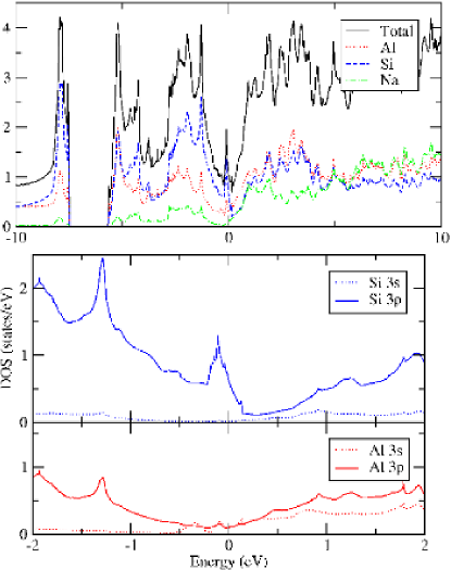
Fig. 3 shows the total, partial, and projected densities of states (DOS) of NaAlSi. The Na contribution near the Fermi level is negligible and thus not shown. Except for a strong dip (“pseudogap”) near the Fermi level and a less severe dip in the to eV range, the DOS hovers around 3 states/eV throughout both valence and conduction bands. Within the pseudogap encompassing the Fermi energy, there is an anomalous sharp and narrow peak with lying on its upper slope, as noted previously by Kuroiwa et al.Kuroiwa et al. (2007) The value of is 1.1 states/eV. We discuss below the FSs of both hole (Si) and electron (Al) character.
It seems clear that the transport properties and low-energy properties (which have not yet been reported), and in particular the superconductivity of NaAlSi, are intimately associated with this sharp and narrow peak in the DOS, which includes the Fermi level. The projected DOS shows the flat bands that give rise to this peak are very strongly Si-derived. There is Al character that turns on just below , but it is relatively small compared to the Si character at , and its magnitude remains low and nearly constant through the peak. There is Al character of the same magnitude in the vicinity of the Fermi level. The top edge of the peak coincides with the flat band along -X at 0.13 eV. The width of the peak, about 0.35 eV, must be due to dispersion and anticrossings that are mostly not visible along symmetry directions and arise from mixing away from symmetry lines of the valence and conduction bands.
Nonetheless, the slope of the DOS at is rather steep, and this may give rise to high thermopower for the material. The standard low-temperature limit of thermopower (the Seebeck coefficient tensor) S in semiclassical Bloch-Boltzmann theory is
| (1) |
The conductivity tensor can be written in terms of the average velocity () product, DOS, and scattering time over the constant energy () surface:
| (2) |
The thermopower thus picks up contributions from the energy variation of three quantities: the dyadic product , , and . Often the energy dependence of is neglected, out of lack of detailed knowledge, though it also can be argued to follow roughly for elastic scattering. The energy dependence of also counteracts the energy dependence of . Nevertheless it is observed that materials with large slope in frequently have large thermopower. For NaAlSi we calculate eV-1. This value can be compared with other materials that have fine structure near the Fermi level: TiBe2, where = 10–12 eV-1 and also is much larger;kyker and MgCNi3 with its very impressive peak very near , for which -15-20/eV-1.rosner2
The energy derivative of diagonal elements of that occurs in Eq. 1 can also be expressed as
| (3) | |||||
where is (a diagonal element of) the inverse mass tensor (second derivative of ) averaged over the constant energy surface. This form makes it clear that the expressions should, for any quantitative estimate, be generalized to two-band form, since the valence and conduction bands have differing signs of their effective masses, and the scattering time—and its energy variation—is likely to be very different for Si-derived covalent valence bands and Al-derived free-electron conduction bands. Measurement of the thermopower, and a quantitative theoretical treatment, would be very useful in extending the understanding of the transport properties of NaAlSi.
III.3 Unusual Fermi surfaces
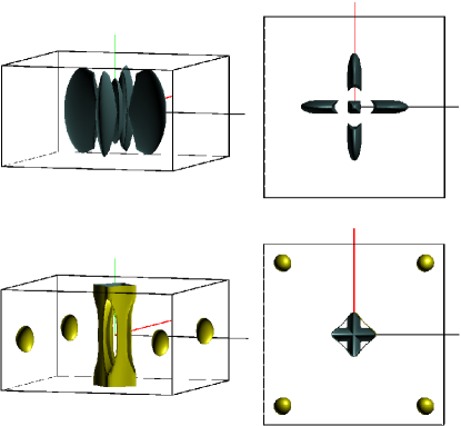
Fig. 4 depicts the calculated FSs. In spite of the generally 2D band structure, the small dispersion of bands at make some of the FSs surprisingly three-dimensional. Electron pockets and hole pockets coexist in the Brillouin zone, with electron and hole concentrations necessarily being equal.
Hole surfaces. Four hole “fan-blade” surfaces lie oriented in the - and -planes. At the center, extending from half way to Z, lies a long and narrow surface with square cross section. The top view allows the origin of these surfaces to be understood. The cross sections in the -plane are of two ellipses that are very anisotropic (in the -plane) and at right angels to each other. Each corresponds to a dispersion that is weak in one direction (the long major axis) and strong in the other (minor axis). These bands would intersect, but in fact are intersected by the electron band that cuts a squarish hole (rotated by 45∘), within which the elongated hole surface inside re-emerges.
Electron surfaces. In the bottom panels of Fig. 4, the squarish electron surface (with variation and resulting holes, shown in the lower two panels of Fig. 4) that cuts the aforementioned hole surface is pictured, and substantiates the discussion provided just above. In addition, there are simple electron ellipsoids centered along the -M lines. It is curious that in a band structure that is for the most part strongly 2D, all the FSs have a rather definite three-dimensional character. Although the bands show little dispersion along -Z, the bands just above the the Fermi level are quite different depending on whether or . In particular, the lowest band along R-A is rather flat, but the lowest conduction band along X-M has a dispersion of nearly 2 eV. Similar comparisons can be made for the bands along -X and Z-R. The dispersion is not nearly as strong near , which is clear from both the band structure and the FS.
Short discussion. It was noted in the Introduction that the NaAlSi structure is the same as the Fe-pnictide “111” structure. Moreover, in both compounds, the relevant bands involve only the (Si-Al-Si or As-Fe-As) trilayer. The top view of the fan-blade surfaces have characteristics in common with those of some of the Fe pnictides,Singh (2008); Mazin et al. (2008) all of which have this same trilayer. The similarity is that the top view of the fan blades (if one ignores the diamond-shaped cutout at the intersection, centered at ) appears to show intersecting FSs, neither of which has the square symmetry of the lattice.
Such occurrence of intersecting FSs, each with lower symmetry than the lattice, has been analyzed for LaFeAsO (a “1111” compound) by Yaresko et al.yaresko A symmetry of the Fe2As2 (also Al2Si2) substructure is a non-primitive translation connecting Fe atoms (respectively, Al atoms) followed by -reflection. This operation leads to symmetries that allow bands to be unfolded into a larger Brillouin zone (that is, a “smaller unit cell” having only one Fe atom) which unfolds the band structure and the intersecting FSs. The NaAlSi FSs appear to have this similar crossing (albeit interrupted by the free-electron bands), and the highly anisotropic dispersion is due to distinct (but symmetry-related) hopping along each of the crystal axes. In this respect NaAlSi may clarify the electronic structure of the pnictides: by analogy, there are separate bands that disperse more strongly along the direction or the direction, and give rise to the intersecting, symmetry-related surfaces. In NaAlSi the bands are much more anisotropic in the plane (approaching one-dimensional), making such character much clearer. A difference that complicates the analogy is that in the pnictides the bands near are derived from the Fe atoms, which comprise the center layer of the trilayer, whereas in NaAlSi the bands under discussion are derived from the Si atoms, which comprise the two outer layers.
III.4 Wannier functions
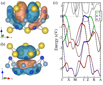
Pictured in Fig. 5 are symmetry-projected Wannier functions (WFs) projected onto Si orbitals. The extension of the WFs shows considerable involvement from nearby Al and Si atoms, and in addition have some density extending into the Na layers. The WF consists of an atomic function, with its density shifted downward by the bonding contribution of Al hybrid orbitals. Beyond the lobes the nearest Si atoms form a bonding lobe that connects to the “small” side of the Al function. The large lobes and the extra contribution from nearby Si atoms are responsible for the largest hopping amplitudes shown in Table 1, although there is some phase cancellation between the lobe and the lobe lying beyond the nodal surface.
The WF has one lobe extended well into the Na layer; this is responsible for the largest hoppings along in Table 1, and they create the large dispersion in the bands seen in Fig. 5(c). Again, the Al atoms contribute with an hybrid orbital, although it appears to be more -like than -like. There is also a “ring” structure below the Al layer, where an hybrid orbital from the Si atoms forms a bonding combination, but it is antibonding with the function on the central Si. The largest contribution to near-neighbor hopping in the Al-Si plane between and or is most likely due to this ring structure, as the lobes are confined to the inside of a square of near-neighbor Al atoms, which are only edge sharing with the nearest Si atoms along vectors. This is the likely reason that all the hoppings along are approximately of the same magnitude. The dispersion which creates the FSs along -Z (seen in Fig. 4) is composed only of the and WFs. This is not caused by the large hoppings, but by smaller hoppings along between and WFs. Without these small hoppings, the band just above is dispersionless along -Z.
| 761 | 60 | |||
| -62 | 60 | |||
| 60 | 60 | -40 | ||
| 128 | 27 | |||
| 361 | 300 | 360 | ||
| 300 | 361 | 360 | ||
| 360 | 360 | 360 | ||
| 12 | 5 | 50 | ||
| 5 | 12 | 50 | ||
| 50 | 50 | 185 |
IV Response to changes
IV.1 Electron-ion coupling
A deformation potential is the shift in an energy band with respect to sublattice atomic displacement. One can freeze in phonon modes to calculate deformation potentials, which at the FS are directly connected to electron-phonon matrix elements.Khan and Allen (1984)
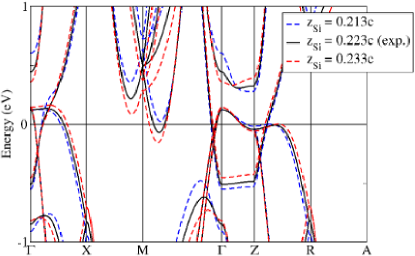
Moving the Si atoms in the direction by 1% of the experimental parameter, such that the tetrahedra surrounding the Al atoms stretch or flatten (while remaining centered on Al), gives an average deformation potential of 0.8 eV/Å over five band positions near the Fermi level. The largest shift is for the ellipsoidal electron pockets, with eV/Å. These ellipsoids disappear when the Si atoms are displaced toward the Al plane (see Fig. 6).
Flattening the Na bilayer, so as to remove the buckling of the Na atoms, requires a (very large) 12% change in the component of the Na atoms. We chose such a large displacement because we do not expect a substantial deformation potential for Na movement. Even this large displacement does not alter very much the valence bands, as expected, and the hole FSs remain virtually unchanged. The conduction bands at the Fermi level however shift appreciably, resulting in a modulation of the electron ellipsoids along (1,1) near M. In addition, the accidental four-band near-degeneracy that is 0.5 eV above at M splits the two separate doubly-degenerate states, opening up a gap of 0.7 eV, which is equivalent to a deformation potential of 0.8 eV/Å (but the bands are not at ).
IV.2 Magnetic susceptibility
The magnetic spin susceptibility is given by
Fixed-spin-moment calculations were conducted to produce an energy-vs.-moment curve, resulting in a susceptibility of eV-1, or emu/mol. This is the exchange-enhanced susceptibility in the Stoner theory, and can be written as
where is the Stoner enhancement factor, is the Stoner parameter, and the bare Pauli susceptibility is equal to . Janak has shown how to calculate within density functional theory,Janak which must be equivalent (within a minor approximation he used) to our approach of using fixed-spin-moment calculations.
With our calculated values we obtain , which translates to eV. Some interpretation of this value of Stoner should be noted. First, falls where most of the states are Si-derived, so for simplicity we neglect Al (and Na, which is ionized). Second, we note that there are two Si atoms in the primitive cell. Thus to get an “atomic value” of , we should use a value of per Si atom. The result then is very roughly eV. This value can be compared to the atomic value for Al (next to Si in the periodic table) in the elemental metal, which is = 0.6 eV.Janak It seems, therefore, that Si in NaAlSi is considerably more “magnetically inclined” than is Al in aluminum. However, the Stoner enhancement overall is not large, indicating relatively modest magnetic enhancement and rather conventional magnitude of magnetic interactions.
IV.3 Comparison to NaAlGe
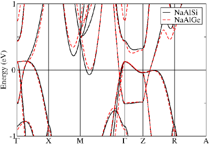
Isostructural and isovalent NaAlGe is not superconducting (above 1.6 K, at least), so it should be instructive to compare its electronic structure to that of NaAlSi. Using its experimental lattice parameters, Westerhaus and Schuster (1979) we have calculated the band structure of NaAlGe, and compared it with that of NaAlSi on a rather fine scale in Fig. 7. The band structures are very similar, the one difference being that the band along -M near M does not cross in NaAlGe. The free-electron band is also identical.
Supposing the tiny bit of FS along -M cannot account for the difference in superconducting behaviors, the factors relevant for electron-phonon coupling will be the difference in mass (Ge is more than twice as heavy as Si) and the difference in electronic character, which can affect force constants and electron-phonon matrix elements. A real possibility is that the pairing mechanism is electronic rather than phononic. In three dimensions purely electronic pairing mechanisms have been attracting serious study (by Sham and collaboratorssham1 ; sham2 for example), but 2D semimetals introduce new features that deserve detailed study.
Another possibility is that these pockets are important, and that superconductivity arises from an enhancement of electron-phonon coupling in these tiny electron pockets from low frequency electronic response, either interband transitions or plasma oscillations, or both. A model in which the electronic response of a 2D electronic superlattice plays a central role in the mechanism has been previously studiedbill1 ; bill2 using a model of parallel conducting sheets separated by a dielectric spacer. This model may be useful as a starting point for understanding NaAlSi.
V Discussion
The classes of materials that contain relatively high temperature superconductorsother continues to expand. Superconductors derived from doped 2D semiconductors pose many of the most interesting issues in superconductivity today. The cuprates and the Fe-pnictides (and -chalcogenides) are strongly magnetic, and comprise one end of the spectrum (though they are themselves quite different). On the other end lie those with little, perhaps negligible, magnetism: electron-doped ZrNCl and HfNCl, and electron-doped TiNCl. There are several other, lower- systems, whose behavior seems different still (hydrated NaxCoO2, Li1-xNbO2, and several transition-metal disulfides and diselenides).
A common feature of most of these systems is that they are 2D and have a small, but not tiny, concentration of charge carriers, often in the range of 0.05–0.15 carriers per unit cell. These materials also have ionic character. NaAlSi differs in that it has carriers—the others have carriers in bands—and is self-doped, a compensated semimetal. We suggest that a useful view of NaAlSi is that it be regarded as arising from an underlying ionic semiconductor, but that it has a small negative gap rather than a true gap. Without the overlap of the valence and conduction bands, it would be a 2D, ionic, and somewhat covalent semiconductor like the aforementioned nitridochloride compounds, which superconduct in the 15–25 K range. Comparing the characteristics of these two classes of superconductors should further the understanding of 2D superconductivity.
VI Acknowledgments
This work was supported by DOE grant DE-FG02-04ER46111, the Strategic Sciences Academic Alliance Program under grant DE-FG03-03NA00071, and by DOE SciDAC Grant No. DE-FC02-06ER25794.
References
- Kamihara et al. (2008) Y. Kamihara, T. Watanabe, M. Hirano, and H. Hosono, J. Am Chem. Soc. 130, 3296 (2008).
- Yamanaka et al. (1996) S. Yamanaka, H. Kawaji, K. Hotehama, and M. Ohashi, Adv. Mater. 8, 771 (1996).
- Shamoto et al. (1998) S. Shamoto, T. Kato, Y. Ono, Y. Miyazaki, K. Ohoyama, M. Ohashi, Y. Yamaguchi, and T. Kajitani, Physica C 306, 7 (1998).
- Yamanaka et al. (1998) S. Yamanaka, K. Hotehama, and H. Kawaji, Nature 392, 580 (1998).
- Shamoto et al. (1999) S. Shamoto, K. Iizawa, M. Yamada, K. Ohoyama, Y. Yamaguchi, and T. Kajitani, J. Phys. Chem. Solids 60, 1431 (1999).
- Yamanaka et al. (2009) S. Yamanaka, T. Yasunaga, K. Yamaguchi, and M. Tagawa, J. Mater. Chem. 19, 2573 (2009).
- Kuroiwa et al. (2007) S. Kuroiwa, H. Kawashima, H. Kinoshita, H. Okabe, and J. Akimitsu, Physica C 466, 11 (2007).
- Bustarret et al. (2006) E. Bustarret, C. Marcenat, P. Achatz, J. Kačmarčik, F. Lévy, A. Huxley, L. Ortéga, E. Bourgeois, X. Blase, D. Débarre, and J. Boulmer, Nature 444, 465 (2006).
- (9) L. F. Mattheiss, E. M. Gyorgy, and D. W. Johnson, Jr., Phys. Rev. B 37, 3745 (1988).
- (10) S. Jin, T. H. Tiefel, R. C. Sherwood, A. P. Ramirez, E. M. Gyorgy, G. W. Kammlott, and R. A. Fastnacht, Appl. Phys. Lett. 53, 1116 (1988).
- Ekimov et al. (1998) E. A. Ekimov, V. A. Sidorov, E. D. Bauer, N. N. Mel’nik, N. J. Curro, J. D. Thompson, and S. M. Stishov, Nature 428, 542 (2004).
- Rosner et al. (2002) H. Rosner, A. Kitaigorodsky, and W. E. Pickett, Phys. Rev. Lett. 88, 127001 (2002).
- Sagayama et al. (2006) H. Sagayama, Y. Wakabayashi, H. Sawa, T. Kamiyama, A. Hoshikawa, S. Harjo, K. Uozato, A. K. Ghosh, M. Tokunaga, and T. Tamegai, J. Phys. Soc. Jpn. 75, 043713 (2006).
- Kuroiwa et al. (2006) S. Kuroiwa, H. Sagayama, T. Kakiuchi, H. Sawa, Y. Noda, and J. Akimitsu, Phys. Rev. B 74, 014517 (2006).
- Shein et al. (2003) I. R. Shein, N. I. Medvedeva, and A. L. Ivanovskii, J. Phys.: Condens. Matter 15, L541 (2003).
- Huang et al. (2004) G. Q. Huang, L. F. Chen, M. Liu, and D. Y. Xing, Phys. Rev. B 69, 064509 (2004).
- Mazin and Papaconstantopoulos (2004) I. I. Mazin and D. A. Papaconstantopoulos, Phys. Rev. B 69, 180512 (2004).
- Giantomassi et al. (2005) M. Giantomassi, L. Boeri, and G. B. Bachelet, Phys. Rev. B 72, 224512 (2005).
- Heid et al. (2007) R. Heid, K. -P.Bohnen, B. Renker, P. Adelmann, T. Wolf, D. Ernst, and H. Schober, J. Low Temp. Phys. 147, 375 (2007).
- Kuroiwa et al. (2008) S. Kuroiwa, A. Q. R. Baron, T. Muranaka, R. Heid, K. -P. Bohnen, and J. Akimitsu, Phys. Rev. B 77, 140503(R) (2008).
- Koepernik and Eschrig (1999) K. Koepernik and H. Eschrig, Phys. Rev. B 59, 1743 (1999).
- Perdew and Wang (1992) J. P. Perdew and Y. Wang, Phys. Rev. B 45, 13244 (1992).
- Westerhaus and Schuster (1979) W. Westerhaus and H. U. Schuster, Z. Naturforsch. 34b, 352 (1979).
- Momma and Izumi (2008) K. Momma and F. Izumi, J. Appl. Cryst. 41, 653 (2008).
- (25) A. B. Kyker and W. E. Pickett, Phys. REv. B 71, 224517 (2005).
- (26) H. Rosner, R. Weht, M. D. Johannes, W. E. Pickett, and E. Tosatti, Phys. Rev. Lett. 88, 027001 (2002).
- Singh (2008) D. J. Singh, Phys. Rev. B 78, 094511 (2008).
- Mazin et al. (2008) I. I. Mazin, D. J. Singh, M. D. Johannes, and M. H. Du, Phys. Rev. Lett 101, 057003 (2008).
- (29) A. N. Yaresko, G.-Q. Liu, V. N. Antonov, and O. K. Andersen, Phys. Rev. B 79, 144421 (2009).
- Khan and Allen (1984) F. S. Khan and P. B. Allen, Phys. Rev. Lett. 29, 3341 (1984).
- (31) J. F. Janak, Phys. Rev. B 16, 255 (1977).
- (32) H. Rietschel and L. J. Sham, Phys. Rev. B 28, 5100 (1983).
- (33) M. Grabowski and L. J. Sham, Phys. Rev. B 29, 6132 (1984).
- (34) A. Bill, H. Morawitz, and V. Z. Kresin, Phys. Rev. B 66, 100501 (2002).
- (35) A. Bill, H. Morawitz, and V. Z. Kresin, Phys. Rev. B 68, 144519 (2003).
- (36) W. E. Pickett, Physica B 296, 112 (2001).