Molecular switch controlled by pulsed bias voltages
Keywords: Density functional calculations, Molecular electronics, Molecular switches, Molecular wires, Molecular mechanics
It was observed in recent experiments that the current-voltage characteristics (IV) of BPDN-DT (bipyridyl-dinitro oligophenylene-ethynylene dithiol) can be switched in a very controlled manner between “on” and “off” traces by applying a pulse in a bias voltage, . We have calculated the polaron formation energies to check a frequently held belief, namely, that the polaron formation can explain the observed bistability. Our results are not consistent with such a mechanism. Instead, we propose a conformational reorientation. The molecule carries an intrinsic dipole moment which couples to . Ramping exerts a force on the dipole that can reorient (“rotate”) the molecule from the ground state (“off”) into a metastable configuration (“on”) and back. By elaborated electronic structure calculations, we identify a specific path for this rotation through the molecule’s conformational phase space. We show that this path has sufficiently high barriers to inhibit thermal instability but still the molecule can be switched in the voltage range of the junction stability. The theoretical IVs reproduce qualitatively the key experimental observations. We propose, how the alternative mechanism of conductance switching can be experimentally verified.
1 Introduction
During the past few years, experiments in the field of “Molecular Electronics” have experienced significant improvements. This made possible the observation of Coulomb blockade [1] and Kondo effects [2] in molecular transistor geometry. Improved statistical methods to access a conductance of molecular junctions have been developed [3, 4]. A spectacular manifestation of molecular low energy excitations has been detected [5] in inelastic current spectroscopy.
Aiming for potential applications, Molecular Electronics holds the vision that functional devices like memory elements, switches, transistors etc. may be realizable by designing suitable molecular complexes. In this spirit, a considerable effort to design and test molecular systems with a controlled switching behavior has been made [6, 7]. The challenge here is a ubiquitous one in the field of Nanotechnology, namely how to build and manipulate a device or a material with full control down to the atomic level. Therefore, one may expect that a solution in one subfield will cross-fertilize exciting developments in many others.
The proposed prototypes for single molecule memory elements can be sorted according to which physical degree of freedom underlies the switching bistability. The three principle categories are: (I) switches with different (meta-)stable charge configurations [8, 9, 10, 11, 12, 13]; (II) conformational switches with molecules exhibiting different stable isomers [14, 15, 16, 17]; (III) conformational switches with molecular reorientations against the contact atoms [18]. Once it is known how to operate a single molecule, arrays of molecules can be addressed as well, which eventually may form an entirely new class of molecular hybrid-materials.
It is very encouraging, that in recent experiments switching has been successfully demonstrated by Blum et al. [19], Keane et al. [20] and Lörtscher and Riel [21]. They have been using a molecular wire of the ”Tour-type”, BPDN-DT, see Fig. 1, which was investigated in several experimental and theoretical works, before [18, 22, 23]. This particular set of experiments has two intriguing features: first, switching is established in a two-terminal device, just employing a pulse in the bias voltage, and second the effect is very stable, so that it has even been observed at room temperature.
Specifically, the BPDN-DT wire shows the following characteristic behavior in experiment [21]: with a very slow (adiabatic) change of the bias, , the current voltage characteristic (IV) is fully reversible for up-sweeping and down-sweeping. However, with faster sweeping rate the adiabatic regime is left and a hysteretic behavior is seen in the IV if is tuned beyond V. The new IV-curve signalizes the existence of a second (meta-)stable state of the molecular junction. One returns to the original curve only by repeating the procedure with inverted bias.
The physical origin of bistability in these experiments has not yet been identified up to now. He et al. [23] attribute it for their experiment in electrochemical environment to a change in the oxidation state of the molecule. A polaron caused bistability was put forward by Galperin et al. [24] also as a possible explanation of switching observed in the break junction experiment by Lörtscher et al. [21] who investigated a freely suspended molecular bridge. On the other hand, Keane et al. [20] argue that the formation of a polaron is not a likely occurrence in their electromigrated break junction experiment. They suspect that rather a bias driven modification of the contacts may be responsible.
Identifying a possible switching mechanism operating for Tour-type molecules is the aim of this work. Our calculations suggest the following picture: the BPDN-DT molecule in vacuum or in between two contacts, Fig. 2, is not susceptible to charging. Unless it is stabilized by counter-charges that are located very close to the bipyridine unit, any excess charge recombines with its images on the electrodes (Fig. 3). This makes polaron-formation (class I) unlikely in the experiments [19, 20, 21] in support of an earlier claim [20].
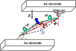
However as we shall demonstrate, the key property for switching, bistability, can originate from a rotational degree of freedom associated with BPDN-DT molecule contacted to electrodes. The inertia that is driving the rotation results from the action of the electrical field (associated with ) on the dipole moment of the dressed bipyridine unit. Two stable configurations can be reached by a double axis -rotation, see Fig. 4 (classes II & III). Our calculations suggest, that the rotation can be performed in such a way, that the rotational barrier is high enough — so both states are stable against temperature — but at the same time this barrier is low enough so that one state rotates into the other under bias voltages V (Fig. 5). The theoretical IV curves (Fig. 6), which one obtains for either state, closely resemble the experimental findings [19, 20, 21].
2 Model and Method
The model setup used for the DFT transport calculations is depicted in Fig. 2. The Au14-clusters mimic the electrodes. Computations based on the density functional theory (DFT) have been performed with the real-space based package TURBOMOLE [25]. Optimized basis sets of triple- quality including polarization functions have been used (exception: IV with a split-valence basis set of double- quality) [26, 27]. The exchange correlation (XC) functional BP86 [28, 29] was employed. Charging analysis and relaxations were checked against a hybrid functional, B3LYP [30].
3 Absence of polarons
In order to investigate the possibility of polaron formation, we have considered the core region of the molecule, only, replacing the Au14 cluster by an H-atom. We compared the electronic structure for the uncharged () and the charged species ( in units of the electron charge ). Energies for the highest occupied (lowest unoccupied) molecular level, HOMO (LUMO), are given in Fig. 3. We first discuss the molecule in the gas phase, “free” molecule. The data indicate, that the LUMO of the positively charged ion () has an energy eV. Upon approaching a metal surface, will increase due to the interaction with the image charge. Assuming, that the excess charge distribution is arranged about the center of the molecule with an extension much smaller than the molecule length, one can give an estimate of the energy change by employing an image charge analysis.We obtained an energy eV for the LUMO after screening. Since it is certain [31], that the workfunction of any uncharged Au-surface is above eV and below eV, one can conclude that the positively charged ion will be neutralized as soon as it makes contact to a Au-surface. By a completely analogous argument for the HOMO of the anion (see Fig. 3), we deduce that also the molecule with is unstable near a Au-surface.
All calculations have been performed with a fully relaxed molecular structure; the charged molecule undergoes a conformational change, which mostly affects the NO2-groups. However, our calculations do not give any indication, that a geometrical deformation could stabilize the ion in the vicinity of the electrodes, see Fig. 3. More precisely, the energy change of the anion’s HOMO (cation’s LUMO) upon structure relaxation is not sufficient in order to induce a level crossing with the Fermi energy. This implies, that the contacted BPDN-molecule does not exhibit a polaron inside a trivial vacuum bounded by the two electrode plates. This is the case in the break junction experiments [20, 21]. Our conclusion does not necessarily apply to experiments in an electrochemical environment [23] if this has a sufficiently large dielectric response.
4 Rotations and bistability
After we have ruled out charge degrees of freedom as a likely origin for bistability, we now turn our attention to mechanisms related to charge neutral conformational changes. Since the control molecule, Fig. 1, did not show hysteresis [19, 21], bistability should involve a (charge neutral) conformational modification of the BPDN-functional unit. An important second requirement is that an external electric field (realized via ) must be able to address the putative degree of freedom. Since the monopole moment of the functional unit remains zero, it should be the force on its dipole moment, , generated by the NO2-groups that pushes one configuration into the other and back; according to our calculations (employing BP functional) 3.0 Debye. Unlike the BPDN-DT, the reference molecule (BP-DT) enjoys the inversion symmetry and, therefore, has a vanishing intrinsic dipole moment. We take this an explanation why its IV does not exhibit hysteretic behavior.
By this reasoning, one is led to look for rotations that take either the entire molecule or at least its BPDN-unit over from a stable ground state configuration (GC, “off”) to another (meta-)stable one (MC, “on”). Any such rotation corresponds to a path in the atomic configuration space of the (extended) molecule. Apart from bistability, the optimal path has to satisfy a number of constraints in order to be a viable candidate for realizing a molecular switch. (i) The energy barrier between GC and MC, , should exceed temperature, , to avoid uncontrolled thermal switching. (ii) In external fields the optimal path should have a continuous deformation so that GC at forward bias, say, and MC at reverse bias become unstable in the sense that . The instability should be reachable at “switching” voltages, , still tolerable for the molecular junction, in experiments Volt. (iii) GC and MC should have two IV curves, and , which can be discriminated from each other.
Giving typical switching voltages Volt, one can estimate the energy barrier separating two states at zero bias. Assuming that the molecule (length Å) forms an angle ca. 45∘ with the bias electric field, we have . Once a dipole, , is flipped in the bias field, the system’s energy gain is , which should be of order if energy mismatch between GC and MC is small compared to . Using Debye, one arrives to an estimate meV.
After an extensive search, we have found a family of paths which is best described as a consecutive one parameter (angle ) rotation about two axes, see Fig. 4. The family parameter is the (average) angle, , that is formed between the longitudinal axis of the molecular wire and the (hypothetical) surface normal of the electrode.
Consider a variation of ground state energy of the system, , with .rotation angle . As may be inferred from Fig. 5 (trace 0V), the example path with satisfies condition (i), since the barrier between GC () and MC () is K which is in rough agreement with the above estimate. (Notice, that the double axis rotation is crucial to obtain consistent energies. Namely, unbalanced single rotations, e.g. about the S-S axis or the C-C axis near the functional unit, give much higher barriers, 200 meV, and thus are ruled out.)
Furthermore, the evolution of the traces depicted in Fig. 5 under the applied homogeneous electric field, , shows that for a path with also condition (ii) is met: the value of at which either GC or MC becomes unstable corresponds to an effective voltage Volt.
Finally, we can show that also (iii) is fulfilled. To this end we have determined the IV curve for the situations GC and MC, again at , with our home made transport package employing the non-equilibrium Green’s function method [32].
5 IV-characteristics
The theoretical IV-curves, Fig. 6, clearly displays two different IV traces which allow to read out the state of the molecular bit, “on” or “off”. They exhibit key features, which now we discuss:
(a) A step-like increase in the current is observed (near 1V). It is mainly due to the molecular orbital HOMO∗ entering the voltage window.
(b) Under the transformation
| (1) |
both IVs are nearly invariant, see insets Fig. 6; Eq. (1) implies that is an even function of . Generally speaking, invariance is an exact property of non-interacting (i.e. non-polarizable) electron systems.111In our discussion we ignore any structure in the density of states, , of the electrodes; i. e. we assume that is independent of energy. In interacting systems, charge localized on the molecule is redistributed as a response to . The polarization produces a change in the effective potential that feeds back into the current carrying orbitals thus giving rise to second order effects, , on the current. Details of the redistribution depend strongly on contacts and the orientation of the molecule in the bias induced -field (in particular its sign). In the present case the molecular junction has an approximate inversion symmetry (see Fig. 4) and therefore violation of is weak.
(c) It is important for understanding the theoretical IV to notice, that symmetry violation is stronger with “on-” than with the “off-”trace (inset Fig. 6), so that at positive but at sufficiently large reverse biases (dashed trace in Fig. 6 is always above the black one). For the -rotations, Fig. 4, the difference relates to a slightly modified contact geometry.
(d) The contact difference between “on-” and “off-” states also manifests itself in the zero bias conductance; according to our calculations and , so . Together with (c), the inequality implies that there must be an intersection of the IVs at a voltage , which is a detail observed in our data, Fig. 6, upper inset.
6 -invariance of -junctions and IV
For a more general class of molecular junctions, which do not share the (approximate) symmetries of the extended molecule, Fig. 4, invariance can be strongly broken if polarization effects become large. In this case the hysteretic features of the IV will be even more pronounced. Indeed, there is an intrinsic residual symmetry of any -junction,
| (2) |
which in reality will be violated but only due to contacts. If the impact of contacts is not too strong, then the approximate validity of Eq. (2) ensures, that the junction’s IV-curves closely resemble the switching characteristic of Fig. 6 (main plot) in the sense that there is a well defined upper (“on”) and a lower (“off”) curve.
7 Discussion
The theoretical IV, Fig. 6 shares all essential qualitative features with the experimental result [21]. For three reasons, a detailed quantitative comparison of absolute values for currents and the characteristic voltages, and , appears quite difficult. (1) Our theoretical analysis implies that the angle determines the switching voltage, , since it controls the effective force () that acts on the intrinsic BPDN-dipole moment facilitating the molecular rotation. Since details of the atomic conformation of the molecular junction realized in experiments are not known, remains largely unspecified. In fact, our atomistic modeling of the contact, Fig. 2, can be only a crude caricature of experimental reality and therefore parameters like are not necessarily very well defined; in addition their statistics may fluctuate between different experiments [19, 21, 20]. (2) Another uncertainty relates to the fact that in experiments the molecule may not be in a fully relaxed conformation. Our preliminary calculations show that depending on whether or not molecular geometries are relaxed, the -traces depicted in Fig. 5 vary, if only in a quantitative way. Moreover, our switching path, Fig. 2, is a particularly simple, one parameter species and there is no reason to expect that it is already optimal. Rather, paths realized in experiments will most likely be somewhat different, i.e. some (smooth) deviations of it. (3) It is a well known fact, that due to the local approximations in the exchange correlation functionals (XC), DFT calculations do not usually give precise quantitative results for conductances [32] or molecular polarizabilities [33]. For this reason, our theoretical results have an intrinsic quantitative uncertainty.
8 Predictions
We close with offering two qualitative predictions that follow from our theoretical analysis: (p1) The “easy axis” rotational degree of freedom of BPDN around the carbon triple bonds, Fig. 1, is crucial for -rotations. If easy rotation is blocked e. g. by molecular design, then the rotational barriers become much higher, switching is more difficult and hysteresis should be suppressed. (p2) The switching voltage, can be modified by dressing the BP-unit, Fig. 1, with other redox groups, e.g. carboxy-groups, COOH, instead of the nitro-groups, NO2. We expect, that the switching voltage decreases when the intrinsic dipole moment of the BP-complex becomes larger. (Here, we have assumed that the change in molecular conformation, which accompanies the exchange of the redox groups, is less important.)
Summarizing, we have identified a two-axis rotation that takes a Tour-type, BPDN-DT, molecular junction from its ground-state conformation (“off”) into a metastable one (“on”). The energy barrier for this process is larger than temperature, but can be controlled by applying a bias voltage. At sufficiently large biases, the molecule undergoes the transition from “off”-state to “on” and reverse, so that it can realize a molecular switch. Our theoretical analysis may explain the pronounced switching behavior observed in recent experiments [19, 20, 21].
Acknowledgments
We gratefully acknowledge helpful discussions with K. Fink, H. Fliegl, M. Mayor, M. Ruben, F. Schramm and Th. Wandlowski. Our particular gratitude belongs to our colleagues at IBM Zurich, E. Lörtscher and H. Riel, for inspiring discussions and for sharing generously unpublished material. This work was supported by the Center of Functional Nanostructures at Karlsruhe University.
References
- [1] S. Kubatkin, A. Danilov, M. Hjort, J. Cornil, J.-L. Brédas, N. Stuhr-Hansen, P. Hedegård, T. Bjørnholm, Nature (London) 2003, 425, 698.
- [2] E. A. Osorio, K. O’Neill, M. Wegewijs, N. Stuhr-Hansen, J. Paaske, T. Bjornholm, H. S. J. van der Zant Nano Lett. 2007, 7, 3336.
- [3] (a) E. Lörtscher, H. Weber, H. Riel, Phys. Rev. Lett. 2007, 98, 176807. (b) C. Li, I. Pobelov, Th. Wandlowski, A. Bagrets, A. Arnold, F. Evers, J. Am. Chem. Soc. 2008, 130, 318.
- [4] (a) L. Venkataraman, J. E. Klare, C. Nuckolls, M. S. Hybertsen, M. L. Steigerwald, Nature 2006, 442, 904. (b) L. Venkataraman, J. E. Klare, I. W. Tam, C. Nuckolls, M. S. Hybertsen, M. L. Steigerwald, Nano Lett. 2006, 6, 458.
- [5] (a) L. H. Yu, Z. K. Keane, J. W. Ciszek, L. Cheng, M. P. Stewart, J. M. Tour, D. Natelson, Phys. Rev. Lett. 2004, 93, 266802. (b) A. N. Pasupathy, J. Park, C. Chang, A. V. Soldatov, S. Lebedkin, R. C. Bialczak, J. E. Grose, L. A. K. Donev, J. P. Sethna, D. C. Ralph, P. L. McEuen, Nano Lett. 2005, 5, 203. (c) H. B. Heersche, Z. de Groot, J. A. Folk, H. S. J. van der Zant, C. Romeike, M. R. Wegewijs, L. Zobbi, D. Barreca, E. Tondello, A. Cornia, Phys. Rev. Lett. 2006, 96, 206801. (d) E. A. Osorio, K. O’Neill, N. Stuhr-Hansen, O. F. Nielsen, T. Bjørnholm, H. S. J. van der Zant, Adv. Materials 2007, 19, 281.
- [6] N. J. Tao, Nature Nanotechnology 2006, 1, 173.
- [7] N. Weibel, S. Grunder, M. Mayor, Org. Biomol. Chem. 2007, 5, 2343.
- [8] W. Haiss, H. van Zalinge, S. J. Higgins, D. Bethell, H. Höbenreich, D. J. Schiffrin, R. J. Nichols, J. Am. Chem. Soc. 2003, 125, 15294.
- [9] F. Chen, J. He, C. Nuckolls, T. Roberts, J. E. Klare, S. Lindsay, Nano Lett. 2005, 5, 503.
- [10] B. Xu, X. Xiao, X. Yang, L. Zang, N. Tao, J. Am. Chem. Soc. 2005, 127, 2386.
- [11] C. Li, A. Mishchenko, Z. Li, I. Pobelov, Th. Wandlowski, F. Würthner, A. Bagrets, F. Evers, J. Phys.: Cond. Matter 2008, 20, 374122.
- [12] (a) M. Galperin, M. R. Ratner, A. Nitzan, Nano Lett. 2005 5, 125; (b) M. Galperin, A. Nitzan, M. R. Ratner, J. Phys. Condens. Matter. 2008 20, 374107.
- [13] D. A. Ryndyk, P. D’Amico, G. Cuniberti, K. Richter, arXiv:0802.2808v1.
- [14] P. E. Kornilovitch, A. M. Bratkovsky, R. S. Williams, Phys. Rev. B 2002, 66, 245413.
- [15] Y. Luo, C. P. Collier, J. O. Jeppesen, K. A. Nielsen, E. DeIonno, G. Ho, J. Perkins, H.-R. Tseng, T. Yamamoto, J. F. Stoddart, J. R. Heath, ChemPhysChem 2002, 3, 519.
- [16] Y. Y. Liang, F. Jiang, Y. X. Zhou, H. Chen, R. Note, H. Mizuseki, Y. Kawazoe, J. Chem. Phys. 2007, 127, 084107.
- [17] A. C. Whalley, M. L. Steigerwald, X. Guo, C. Nuckolls, J. Am. Chem. Soc. 2007, 129, 12590.
- [18] P. A. Lewis, C. E. Inman, F. Maya, J. M. Tour, J. E. Hutchison, P. S. Weiss, J. Am. Chem. Soc. 2005, 127, 17421.
- [19] A. S. Blum, J. G. Kushmerick, D. P. Long, C. H. Patterson, J. C. Yang, J. C. Henderson, Y. Yao, J. M. Tour, R. Shashidar, B. R. Ratna, Nature Materials 2005, 4, 167.
- [20] Z. K. Keane, J. W. Ciszek, J. M. Tour, D. Natelson, Nano Lett. 2006, 6, 1518.
- [21] E. Lörtscher, J. W. Ciszsek, J. Tour, H. Riel, Small 2006, 2, 973.
- [22] M. Elbing, R. Ochs, M. Fischer, C. v. Hänisch, F. Weigend, M. Köntopp, F. Evers, H. B. Weber, M. Mayor, Proc. Nat. Accad. Sci. USA 2005, 102(25), 8815.
- [23] J. He, Q. Fu, S. Lindsay, J. W. Ciszek, J. M. Tour, J. Am. Chem. Soc. 2006, 128, 14828.
- [24] M. Galperin, M. A. Ratner, A. Nitzan, A. Troisi, Science 2008, 319, 1056.
- [25] R. Ahlrichs, M. Bär, M. Häser, H. Horn, C. Kölmel, Chem. Phys. Lett. 1989, 162, 165.
- [26] A. Schäfer, H. Horn, R. Ahlrichs, J. Chem. Phys. 1992, 97, 2571.
- [27] A. Schäfer, C. Huber, R. Ahlrichs, J. Chem. Phys. 1994, 100, 5829.
- [28] A. D. Becke Phys. Rev. A 1988, 38, 3098.
- [29] J. P. Perdew, Phys. Rev. B 1986, 33, 8822.
- [30] A. D. Becke, J. Chem. Phys. 1993, 98, 5648.
- [31] Y. Umeno, Ch. Elsässer, B. Meyer, P. Gumbsch, M. Nothacker, J. Weissmüller, F. Evers, Europhys. Lett. 2007, 78, 13001.
- [32] (a) F. Evers, Weigend, F.; Köntopp, M. Phys. Rev. B 2004, 69, 235411. (b) A. Arnold, F. Weigend, F. Evers, J. Chem. Phys. 2007, 126, 174101.
- [33] M. van Faassen, P. L. de Boeij, R. van Leeuwen, J. A. Berger, J. G. Snijders, Phys. Rev. Lett. 2002, 88, 186401.

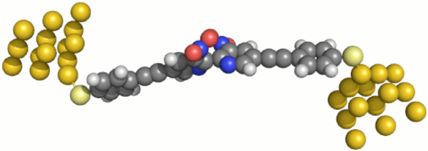
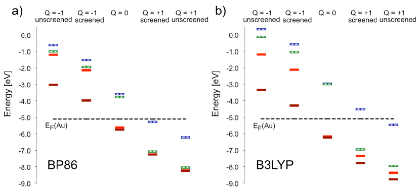

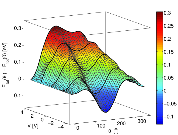
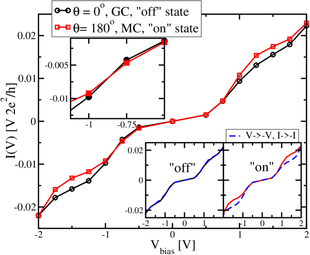
Table of Contents
Recent experiments have identified a specific molecular wire (bipyridyl-dinitro oligophenylene-ethynylene dithiol), BPDN-DT that can be operated as a molecular memory element. Our theoretical work explains the mechanism by which the memory is conserved. At its heart it is a two-axis rotation of the molecule’s functional unit (see Figure). The theoretical current-voltage characteristics reproduces the experimental observations.
ToC keyword: Molecular switches
Velimir Meded, Alexei Bagrets, Andreas Arnold, and Ferdinand Evers∗
Molecular switch controlled by pulsed bias voltages
