ADC non-linear errors correction in thermal diagnostics for the LISA mission
Abstract
Low-noise temperature measurements at frequencies in the milli-Hertz range are required in the LISA (Laser Interferometer Space Antenna) and LISA PathFinder (LPF) missions. The required temperature stability for LISA is around 10 K Hz-1/2 at frequencies down to 0.1 mHz. In this paper we focus on the identification and reduction of a source of excess noise detected when measuring time-varying temperature signals. This is shown to be due to non-idealities in the ADC transfer curve, and degrades the measurement by about one order of magnitude in the measurement bandwidth when the measured temperature exhibits drifts of K s-1. In a suitable measuring system for the LISA mission, this noise needs to be reduced. Two different methods based on the same technique have been implemented, both consisting in the addition of dither signals out of band to mitigate the ADC non-ideality errors. Excess noise of this nature has been satisfactorily reduced by using these methods when measuring temperature ramps up to 10 K s-1.
pacs:
07.20.Dt, 07.87.+vI Introduction
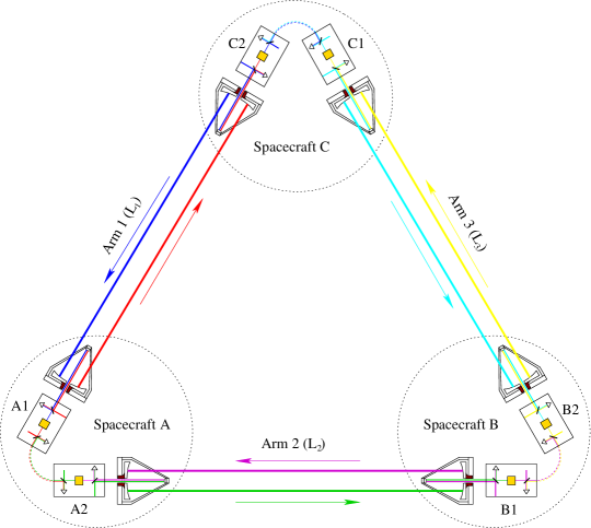
LISA (Laser Interferometer Space Antenna) is a joint ESA-NASA space mission conceived to detect Gravitational Waves (GWs) bender . LISA consists in a constellation of three spacecraft in the vertexes of an equilateral triangle 5 million kilometres to the side. The constellation orbits the Sun following the ecliptic, some 20 degrees (45 million kilometres) behind the Earth. Each spacecraft houses two proof masses in nominal free fall, and laser links are established between spacecraft —see Figure 1. The role of the links is to enable interferometric measurements of relative distance and acceleration variations between pairs of proof masses in distant spacecraft. This is how LISA will detect GWs, since they show up as tidal forces (or geodesic deviations in the language of General Relativity Theory) in the region where the detector is.
Expected GW signals are extremely weak sources , hence severe requirements must be imposed on the proof mass residual acceleration noise to ensure LISA meets its GW detection objectives. These are defined in terms of spectral density lisasrd :
in the frequency band from 0.1 mHz to 0.1 Hz, which is where optimum GW detection performance can be obtained with interferometer arm-lengths of 5 million kilometres lobo.cqg92 .
The conditions in Equation (I) are not only very demanding, they cannot be directly put to test in an earth based environment. The reason is of course the impossibility to maintain a physical system in accurate free fall near the Earth’s surface during periods of several hours, as required for measurements in sub-milli-Hertz frequency bands. This fact motivated ESA, the European Space Agency, to fly a technology precursor mission to secure proper working of the key technologies needed by LISA. Such technology mission goes by the name LISA PathFinder (LPF), and its launch date is scheduled for 2011. LPF is a squeezed version of one LISA arm: its length is downscaled to 30 cm, and the two proof masses are housed in a single spacecraft. Noise requirements in LPF are relaxed by about an order of magnitude relative to those of LISA. Also, the Measuring Bandwidth (MBW) in the LTP (LISA Technology Package, the main instrument on board LPF) is reduced to the range between 1 mHz and 30 mHz. Because of its small dimensions, LPF cannot work as a milli-Hertz GW detector; rather, LPF is a noise monitor intended to understand and properly model its sources anza .
One of such sources of noise, which can limit the performance of LISA, is temperature fluctuations. Thermal stability is necessary to ensure the stability of the optical elements properties in the Optical Metrology System (Optical Bench, mirrors, beam-splitters, etc.), as well as of the proof masses’ environment, where such effects as radiometer and/or radiation pressure fluctuations will cause random accelerations if the temperature fluctuates. This happens in LISA and LPF alike, and the maximum tolerable levels of temperature fluctuations can be derived from estimates of the magnitude of their contribution to the total instrument noise, and (conventionally) assuming that they should contribute not more than 10 % to the total. This generates a requirement in temperature stability for LISA of bender
| (1) |
in LISA’s MBW, i.e., from 0.1 mHz to 0.1 Hz. Consequently, measurements capable to discern such small temperature fluctuations are needed. In LPF, the requirements being relaxed as described above, the temperature stability is also less severe on.ground.tests :
| (2) |
in the frequency band from 1 mHz to 30 mHz. In order to make meaningful temperature measurements, the measuring system must be quieter than this figure, and again 10 % of the above is required for it, i.e.,
| (3) |
The LTP temperature monitoring system has already been designed and tested fee.paper —see also Section II below— and it works. However, a small excess noise has been detected at frequencies around the milli-Hertz when the measured temperature drifts with time. This effect does not pose a serious problem in the LTP, as it only shows up at very low frequencies ( mHz) and in the presence of somewhat high temperature drifts, K s-1. In LISA the MBW stretches down to 0.1 mHz feedback.paper , and even weaker temperature drifts are likely to significantly deteriorate the performance of the measuring system. As we shall see, its origin has been traced to non-linearities of the Analog-to-Digital Converters (ADC).
This paper focuses on the identification and reduction of this excess noise. It is organised as follows: Section II briefly describes the temperature measurement system which will actually fly in LPF. Section III delves into the details of a potential problem with the non-idealities of the ADCs. In Section IV we present experimental evidence that the observed excess noise can indeed be attributed to the ADCs non-ideal response, and also two different ways to reduce that noise are analysed. In Section V we give details of the experimental setups, tests carried through to assess the quality of the proposed methods, and results. Finally, Section VI highlights the most relevant results and the prospects of their applicability for LISA.
II Temperature measurement system description
In this section the temperature measurement system is briefly reviewed. Details can be found in fee.paper . The functional block diagram of the system is given in Fig. 2.

The temperature signal, , coming from a Wheatstone bridge is modulated by a square wave signal of angular frequency ( = 6.25 Hz) to avoid the 1/ noise of the Instrumentation Amplifier (IA). The modulated signal is amplified by the IA and low-pass filtered to avoid aliasing. The signal is then quantised by a 16-bit ADC. Once the signal is digitised, a digital demodulation takes place: samples are averaged during either polarity of the modulating square wave, and the averaged value of one polarity is subtracted from that of the other one —see schematics in Fig. 2. This process results in a noise equivalent temperature for dc signals of
| (4) |
at frequencies down to 0.1 mHz feedback.paper ; fee.paper .
The signal coming from the analog circuit of the front-end electronics (FEE) is quantised by an ADC. Only one type of ADC suitable for this purpose has been certified for use in space applications; it is a 16-bit capacitor based Successive Approximation Register (SAR). Limitations in the performance of the system at low frequencies (milli-Hertz range) when slowly drifting input signals (V s-1) are quantised are related to the non-idealities of such ADCs, as will be shown below.
III Non-ideal quantisation noise
In this section we analyse the ADC non-linearity errors, and how they perturb the temperature measurements.
Quantisation is inherently a non-linear process. By construction, the values of the analog function are rounded up to the closest ADC step, so that even an ideal ADC generates output errors associated to the differences between the real and quantised values of the signal. In an ADC jespers the step size, or Least Significant Bit (LSB), is defined by
| (5) |
where is the number of bits of the ADC, and is the maximum voltage (full-scale) the ADC can quantise. When a large number of bits is considered the error introduced by the quantisation process is usually treated as an independent random variable with uniform probability density function (pdf) and white spectral density jespers .
In a real ADC, however, the quantisation steps are not uniform due to mismatches in the internal topology of the ADC; more specifically, tolerances in the capacitors of the SAR array hoeschele ; analog.dev.book ; arpaia —see Figure 3. Such non-uniformity is specified with two parameters: Differential Non-Linearity (DNL) and Integral Non-Linearity (INL) errors. The DNL is defined as the deviation between two adjacent transition points of the quantisation ladder and an LSB, or Michaeli2008 ; Marc1997
| (6) |
where is the output value of the -th quantisation code.
The additional noise related to the DNL errors can be reduced by suitable dithering carbone94 ; gray93 ; sch ; wagdy96 . The inherent ADC noise plus FEE noise can be considered in this case as a dither source, which appears to be enough to make the DNL negligible in practice —see Section III.3 below.
On the other hand, the INL error is defined as the discrete integral of the DNL, i.e.,
| (7) |
and can be understood as the difference between the real and the ideal ADC transfer curves —see Figure 3. The noise introduced by this error is usually less noticeable, although much more difficult to reduce. In this paper we focus on how to do this, since the INL is the one limiting the performance of the measurement when slowly drifting input signals are present. This is a common situation in LTP temperature measurements.
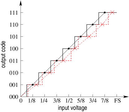
Experimental results —see Section III.4— obtained with the temperature measurement system reflect the problem depicted in Figure 3, which shows up as excess noise in the spectrum. Such noise could not be attributed to actual temperature fluctuations since sensors were placed in a thermal environment where fluctuations were efficiently screened out on.ground.tests , hence such behaviour may not be due to variable temperatures. Analog noise or interferences coming from the signal processing chain (Wheatstone bridge, amplification, low-pas filtering) were also discarded as possible sources of the extra noise. Finally, the excess noise disappears when a dc temperature value (i.e., not drifting with time) is measured 111 For instance, using a high-stability resistor instead of a sensor. —see Figure 6. All in all, the origin of the excess noise has been identified as due to INL errors of the ADC. In the following we present more quantitative arguments confirming this hypothesis.
III.1 ADC bit error description
We first analyse the effect of a faulty bit in a SAR ADC on the performance of the measurement. For this, a simple ADC model is considered. The analog-to-digital conversion is done (in SAR ADCs) by comparing the sampled signal with an analog voltage generated by a Digital-to-Analog Converter (DAC) and a SAR hoeschele . The topology of the DAC is based on a switching capacitor bank composed by 16 capacitors, scaled from to , where defines the Most Significant Bit (MSB) and defines the LSB. The DAC output voltage is jespers
| (8) |
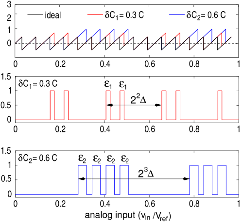
where is the binary digit ( stands for the LSB and for the MSB); it is set to 0 or 1 depending on the sampled voltage, and is the number of bits of the ADC. An error = in the -th capacitor results in an error in the DAC output when the corresponding bit is set to 1. The voltage error induced by a faulty -th bit is therefore
| (9) |
where is the ideal LSB.
The erroneous bit produces a superimposed periodic pattern in the quantisation error of the ADC with 1 LSB of amplitude when the input voltage varies between 0 and , and exhibits a periodicity with the ADC input voltage of . An example of this is shown in Figure 4 where it can be seen how the faulty bit introduces a long period component superimposed on the typical sawtooth error function of an ideal ADC.
III.2 Dither signal effect in ideal quantisers
When a dither voltage, , with a certain probability density function (pdf), , is added to the input signal of the ADC, , the average quantisation error observed at the ADC output, , is given by wagdy89c
| (10) |
where is the quantisation error of an ideal ADC. If we define the Fourier transform in voltage domain by 222 is the Fourier-conjugate variable of , and is accordingly measured in volts-1.
| (11) |
and apply it to Eq.(10), the following ensues:
| (12) |
The quantisation error for an ideal ADC (a sawtooth waveform of amplitude /2 —see Figure 4) is a periodic function of with period . It can be expanded in Fourier series:
| (13) |
and its Fourier transform is
| (14) |
where is Dirac’s -function. If we consider zero-mean Gaussian noise as the dither voltage, its pdf and its Fourier transform are, respectively,
| (15) | |||||
| (16) |
where is the dither variance. Substituting now Eqs. (14) and (16) into Eq. (12) and taking the modulus, we obtain
| (17) |
From Eq. (17) we note that the Gaussian dither signal, , low-pass filters the quantisation error —see Figure 5, top. For instance, for = the attenuation of the first term in the series is 2.7. In our case, we have a 16-bit ADC with =10 V, quasi-white noise at the input of the ADC of V Hz-1/2 and a noise-equivalent bandwidth (NEBW) of 1.2 = 600 Hz, where is the cut-off frequency of the anti-alias filter fee.paper . Thus, and are readily calculated, i.e.,
| (18) | |||||
| (19) |
In our specific case, , hence the quantisation noise from the ideal ADC should be suppressed by the inherent noise of the analog processing chain which acts as a filter to the ideal quantisation error. This can be very clearly seen in Figure 5, top, which shows the errors of an ideal ADC (vertical lines) alongside the equivalent low-pass filter profile (dashed trace) achieved by means of Gaussian dither with = .
III.3 Dither signal effect in non-ideal quantisers
The error of a real ADC is formed by the ideal quantisation error function —see Eq. (13)— plus a term related to the non-idealities of the ADC —see Figure 4. Thus,
| (20) |
where and are the ideal quantisation error and the quantisation error due to the faulty bits, respectively. As seen in the previous section, the ideal quantisation error is filtered out by the analog noise in the measurement chain, which acts as a dither signal of Gaussian pdf. Instead, the quantisation error due to the non-ideality of the ADC is not reduced by the same analog noise, which causes it to show up as extra noise. In this section we show how it can be identified in the temperature measurements, and how it limits the performance of the system.
The modulus of the Fourier transform of the non-ideal noise for a single defective bit, , say, is wagdy96
| (21) |
where is given in Eq. (9). The effect of Gaussian dither on is readily calculated with Eq.(12):
| (22) |
Equations (21) and (22) are plotted in Figure 5 (centre and bottom). The plot in the centre corresponds to errors associated to = 0, i.e., the LSB. Here, the fundamental period is . The plot in the bottom shows the same for = 3 (the 4-th bit) with a fundamental period of 16. For each plot, the low-pass filter generated by Gaussian dither of = is also plotted (dashed lines). It can be noticed that this dither signal suffices to suppress the noise associated to a faulty LSB, = 0 (this corresponds to the DNL effect which, is readily mitigated). However, it cannot attenuate the low frequency lines due to errors in the higher bits. In fact, when = 3 the dithering with = is clearly insufficient.
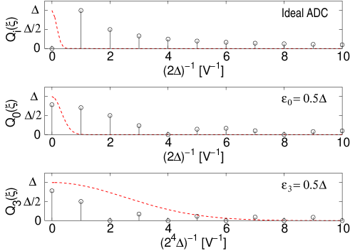
From Figure 5 we note how faulty bits introduce spectral components in the measurement if the signal spans a large enough fraction of the range of the ADC transfer curve. Conversely, if the input signal is a constant dc then no extra noise will be seen, since no bit, whether faulty or not, will change its state. Therefore, the INL effect becomes perceptible in our system only when the input signal runs through a sufficiently wide fraction of the ADC range.
III.4 INL effect on general signals
As we have just seen, when the input signal, , is not a dc constant (e.g., a ramp), the errors related to the INL of the ADC tend to introduce low frequency noise components which degrade the performance of the system. In fact, this is seen to happen in our device for voltage variations in the order of few milli-volts. Moreover, if the input signal changes rate, i.e., then the frequency components introduced by the INL errors spread across the frequency band.
In order to deal with non-constant signals and to estimate INL induced noise, a simplification is expedient. First, let us assume the input signal is a straight line for a certain time interval, i.e.,
| (23) |
where is the initial value of the signal , and is the slope of the input signal (V s-1). If we note the usual time-frequency Fourier transform of the non-ideal quantisation noise, it immediately follows from Eq. (23) that
| (24) |
In this case, Eq. (21) becomes
| (25) |
and the main frequency component for an ADC with an error in the -th bit is located at
| (26) |
Before we proceed further, a technical comment is in order. In several equations above, Dirac -functions appear. They are the result of infinite length integration intervals in Fourier transform calculations, which are of course idealisations. In any practical situation, such intervals are limited to the experimentally available data ranges, so that the -functions are actually sinc-functions: they have identical centre points but spread around those centres depending on the integration interval lengths. In order to make sense of e.g. Eq. (25) we must ask which is the minimum required integration time to obtain a meaningful spectrum or, in other words, which is the minimum duration, of the ramp signal in Eq. (23). This is easily inferred from the frequency of the lowest spectral line in Eq. (26): for a conventional ten cycle integration time we get
| (27) |
These considerations apply to the analysis of the ADC response to signals which drift slowly with time, where slow drift means such signals can be conveniently approximated by a series of concatenated ramps with suitable slopes, and lengths complying with Eq.(27). In these circumstances, we can generalise Eq. (26) as follows:
| (28) |
-
•
High-slope signals at the ADC input translate into high-frequency components at the output of the ADC.
-
•
Errors in the higher bits show up as noise at low frequency.
-
•
Consequently, high-slope input signals combined with errors in high bits may show as noise peaks in the measurement bandwidth.
-
•
The fundamental frequency associated to a faulty bit varies with the variations of , hence the error in a faulty bit spreads across the frequency band when .
The above can be validated by looking at real data from our LTP temperature measurement system. We took a long time series of temperature data, about 4105 seconds, and subdivided it into shorter stretches of 16 000 seconds. With this, we calculated the Short-Time Fourier Transform (STFT) oppenheim , also known as spectrogram, and plotted the results as shown in Figure 6 —see caption for details. The data are amenable to the analysis described above, and the results indicate the presence of the foreseen frequency peaks associated to faulty bits. They are clearly visible in Figure 6, bottom graph, as the darker areas, which show how the fundamental frequency of the INL errors for different faulty bits is varying with time, and accurately tracing the curve shown on the top left plot. A straightforward fit to the first equation (28) permits the identification of the corresponding faulty bit, thus confirming that the extra noise in the temperature measurements is indeed due to the INL errors of the ADC.
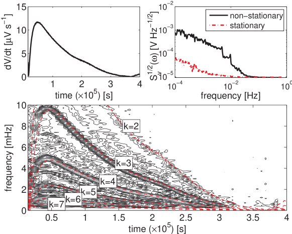
Once the problem has been identified, we focus on possible solutions to fix it. The following section describes two different methods tested successfully to avoid the consequences of INL errors in real ADCs.
IV Mitigation of INL errors
Two different techniques have been used to deal with the non-linearities of the ADC. The first is based on the injection of Gaussian noise out of the MBW, taking advantage of the oversampling involved in the measurement. The second is based on the addition of a triangular wave of high frequency to the signal quantised by the ADC gatti1963 . The following sections describe both techniques as well as their practical implementation.
IV.1 Gaussian noise signal injection
In Section III.2 we saw that Gaussian noise can be used as a dither signal in order to mitigate the non-idealities of the ADC transfer curve. We have also seen that the amount of noise generated by the measurement system itself () is not enough to suppress the periodic components of erroneous bits for 2 —see Fig. 6. Thus, a natural solution is to add more Gaussian noise to the ADC input. Obviously, this noise should be added out of the MBW in order not to disturb the frequency range of interest, which is in the milli-Hertz range. The ADC sampling frequency is 38.4 kHz, thus leaving a large frequency slot to accommodate the required additional noise. Care must however be taken to also place it away from the fundamental frequency of the modulating square wave (and its harmonics) so as to avoid bringing the Gaussian noise back into the MBW in the demodulation process. The required amount of noise to be injected, characterised by , basically depends on the input signal slope, , and on the frequencies of interest, and is limited by the digital processing performed after quantisation —see below. Figure 7 shows the relationship between the input signal slope and the main frequency component for each of the faulty bits. It is useful to identify the faulty bits potentially affecting the measurement as a function of the input signal drifts.
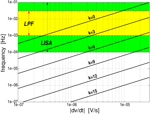
Once the problematic bits are identified, the needed amount of Gaussian dither must be calculated. For this, we define the needed to filter out the noise components associated to the -th faulty bit. If we (conventionally) adopt a damping factor of 10 for the first harmonic then is easily derived from the condition (see Eq. (22))
| (29) |
whence
| (30) |
Gaussian noise dither: practical implementation
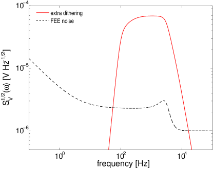
In this section we briefly describe the hardware implementation of the Gaussian dithering scheme. The circuit diagram is given in Fig. 8: the first stage amplifies the noise of an operational amplifier (OP-07 analog.devices ); the second stage is a high-pass filter of 4-th order (two Sallen-Key filters in cascade) with a cut-off frequency of 100 Hz; the third stage is an adder that sums the signal of interest (the amplified output of the Wheatstone bridge) to the dither signal. In the fourth stage, the sum of signal and dither are low-pass filtered with a 4-th order low-pass filter (again, two Sallen-Key filters in cascade) with cut-off frequency 3 kHz. The output of this chain is fed to a 16-bit SAR ADC. The noise shape of the dither signal is given in Fig. 9 (solid trace) where the characteristic frequencies of the high- and low-pass filters are clearly visible.

As mentioned in Section II, the amount of Gaussian dither must be kept under control to avoid excessive noise folding back into the MBW during the digital demodulation stage. The limit of the usable Gaussian noise amplitude, , can be easily estimated assuming a flat spectrum, , from (the corner frequency of the high-pass filter) to (the corner frequency of the low-pass filter). The demodulation by a square wave of frequency entails a certain gain at dc of the odd harmonics of of the dither noise which, under the just mentioned assumption, results in the following oppenheim :
| (31) |
where is the floor function, e.g., is the largest integer smaller than .
In order to cut down the noise leaking into the MBW, i.e., at dc in practice, we again impose a requirement that it be less than 10% of the floor noise in the absence of ADC errors, , i.e.,
| (32) |
In our case, Hz, kHz, and Hz, so that the -sum in Eq. (31) is approximately 0.015, hence 0.015 . The value of is V2 Hz-1 in the MBW. The maximum value for compliant with the criterion Eq. (32) is therefore V2 Hz-1, which corresponds to 0.5 mV.
In Section V, we present the tests and results obtained with this technique.
IV.2 Triangular wave dither
Another implemented and tested technique consists in using a deterministic signal instead of random Gaussian noise as the dither signal. Different signals can be used for this purpose, but for simplicity we have used a triangular wave form in the generation of the signal —see below. In this section we describe the theoretical basis and the hardware implementation details.
The dither signal is now a triangular wave, which can be represented by the Fourier series
| (33) |
where and are the amplitude and the frequency of the triangular wave, respectively —see Fig. 11. Its pdf is papoulis
| (34) |
whose Fourier transform is
| (35) |
As shown in Section III, the averaged quantisation error is
| (36) |
Eq. (36) is graphically evaluated in Figure 10 for different faulty bits and triangular wave amplitudes.
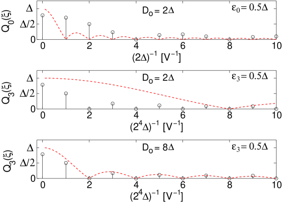
Like we did with the Gaussian noise, we can give an expression to determine the required triangular wave amplitude, , to attenuate the effect of the -th bit:
| (37) |
There is no closed form solution to Eq. (37) for the amplitude of the triangular wave, which requires numerical evaluation in each specific case. The amplitude needed to attenuate the errors coming from the =6 bit is 20 mV.
Triangular wave dither: practical implementation
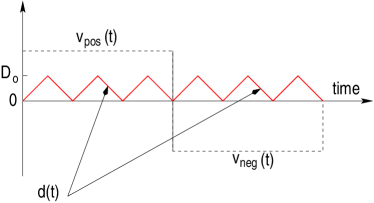
Figure 11 shows the triangular wave added to the system. It is important to note that the addition of the triangular signal will not perturb the temperature measurement within the MBW. The digital demodulation involved in the measurement —see Sec. II— is done by averaging 6144 samples: 3072 during one polarity and 3072 during the opposite polarity. Afterwards they are subtracted and divided by 2. Thus, if we inject exactly the same signal in both polarities the net contribution of the added dither signal to the output is zero —see Eq. (38).
The output signal after the digital processing is
| (38) |
where is the triangular wave —see Fig. 11— and an overbar ( ) means average over 3072 samples.
Eq. (38) indicates that there is no limit on the amplitude of the triangular dither, provided triangular waves in both polarities are identical. Therefore that non-linearities of MSBs can be reduced without degrading the measurement. This happens for an analog dither signal, but ours is actually generated with a DAC, which imposes some limits on the validity of the previous statement —see below.
The circuit which implements the triangular signal is shown in Figure 12, and consists in an 8-bit up-and-down counter followed by a 12-bit DAC where only the 8 LSBs are used. The circuit is configured such that the quantisation step of the DAC closely matches that of the 16-bit ADC. Mismatches here result in actual performance diverging from the predictions of the theoretical analysis described above.
The output signal from the DAC is added to the signal of interest and both are low-pass filtered (a 4-th order Sallen-Key filter with a cut-off frequency of 3 kHz), then quantised by the 16-bit SAR ADC. The triangular wave is low-pass filtered to eliminate high-frequency components related to the digital quantisation of the DAC. Nevertheless, the previous analysis is still valid since the fundamental frequency of the triangular wave is 50 Hz and the low-pass filter cut-off frequency is 3 kHz. Thus, the dither signal will go almost unaltered through the filter (except for some distortion in its high-frequency components).

V Test set-up and results
Both methods described in Section IV have been put to test. For comparison, a 24-bit Delta-Sigma ADC (LTC2440 linear.tech ) which, in principle, should exhibit less non-linearity problems, has also been tested. The two dither techniques under study have been tested using exactly the same electronics, the same 16-bit SAR ADC AD977 analog.devices 333 Actually, the ADC used for the space model is the Texas Instruments ADS7809 which is based in the same structure., and under the same input signal conditions. In this section first we give a brief description of the test set-up and, then, the obtained results are presented.
V.1 Test set-up
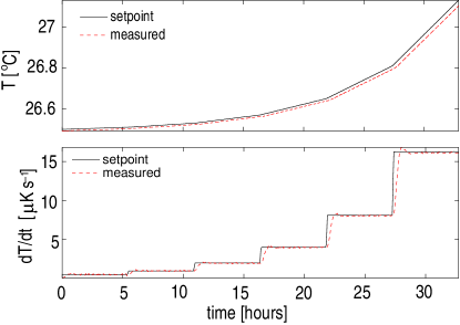
The test set-up is composed by different parts. Temperature sensors are placed inside a thermal insulator designed to screen out ambient temperature fluctuations to the required level in the MBW, i.e., K Hz-1/2 for mHz on.ground.tests . A temperature control is included to implement different temperature profiles inside the insulator; basically, a set of temperature ramps with different slopes is generated in order to assess whether or not the methods to overcome the INL errors of the ADC work —see Figure 14. The temperature control consists in a heater commanded by a programmable power supply which is in turn controlled by the computer calculated value of the difference between the desired temperature and the actual measurement —see Figure 13.
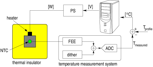
The nominal and actual profiles are shown in Figure 14. The experiment has been repeated for the two dithering techniques, and for the 24-bit Delta-Sigma ADC as well. Prior to that, the 16-bit SAR ADC with no dither signal was tested in order to provide a reference measurement with the INL effects in it.
V.2 Experimental results
The power spectral density in the different tested configurations (no dither, Gaussian noise, triangular wave and 24-bit Delta-Sigma ADC) are given in Fig. 15 for three different slopes, more specifically, for 1, 4 and 8 K s-1. The measurements performed with the 16-bit SAR ADC are clearly affected by the INL errors when no dither signal is used. The noise in the MBW increases by more than one order of magnitude when slopes are around 1 K s-1 and above. Figure 15 shows how the INL errors appear in the MBW, spanning wider frequency regions as slopes increase, thus confirming the predicted behaviour. For instance, when the slope is 4 K s-1 the INL effect is only noticeable at frequencies below 6 mHz, while for a slope of 8 K s-1 the noise appears at frequencies as high as 10 mHz.
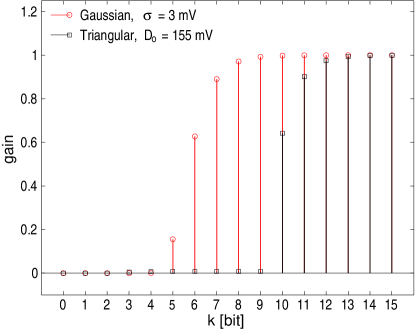
When the dither signal is Gaussian noise, the INL effects can be satisfactorily reduced down to 1 mHz for drifts under 8 K s-1. Looking up Figure 7, we see that faulty bits up to = 5 will create additional noise in the band. Then, using Eq. (30), we find that the necessary dither requires 22 , or 3 mV. This is however a factor of 6 larger than the maximum estimated after Eq. (32), which means some extra noise will be added to the system floor noise, if we insist on applying a = 3 mV dither, as discussed in Section IV.1. We did take this option, with the result that the floor noise becomes a factor 1.5 larger than nominal [in good agreement with predictions calculated using Eq. (31)], with the advantage that good damping of the ADC’s INL errors obtains.
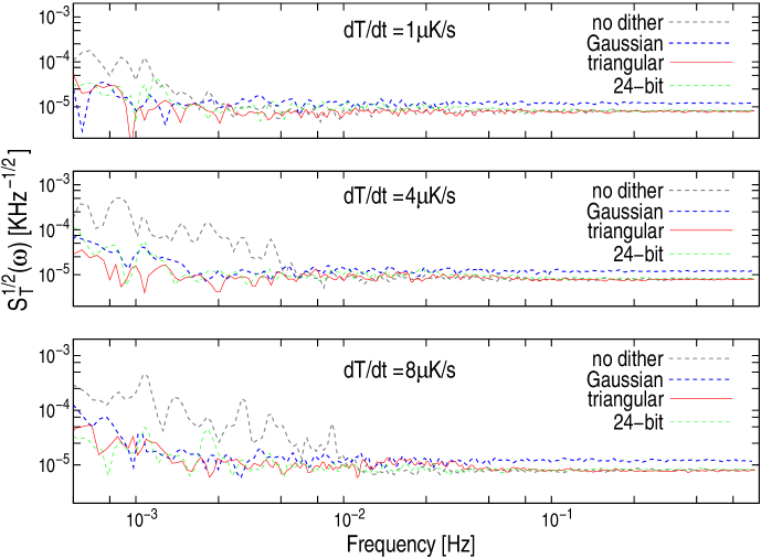
The use of a triangular wave as the dither signal appears as the most robust option to deal with the non-idealities of the ADC: on the one hand, the floor noise is left untouched and, on the other hand, immunity to faulty bits and high signal slopes can be tuned essentially at will. The 24-bit Delta-Sigma ADC exhibits a behaviour similar to that observed in the measurements performed by the 16-bit ADC with added dither signals. Non-linearity errors in this ADC are not noticeable when measuring signals drifting up to 8 K s-1. The generated triangular wave had the following properties: =155 mV and a period of 20 ms, which is an integer sub-multiple of the duration of each polarity (80 ms) —see Figure 11. This amplitude is almost 8 times higher than the one estimated towards the end of Section IV.2 (20 mV) to attenuate errors up the = 6 bit. This means that immunity to faulty bits under higher temperature drifts is accomplished. Figure 16 provides a clear display of the superiority of triangular wave over Gaussian noise dither.
Summing up, Figure 15 confirms the analysis in this paper, and shows that when slopes of 10 K s-1 are present, the effects of the non-idealities can be made negligible by use of proper dither. For higher slopes, e.g., 16 K s-1, some increase in the power spectrum near one milli-Hertz is detected. We believe this is probably due to the relative simplicity of the model used. Further research is ongoing to clarify these matters. Nevertheless, such drifts look unlikely both in LISA and LPF.
VI Discussion
Temperature diagnostics measurements in LISA and LISA PathFinder must meet very demanding requirements: very low noise, a few K Hz-1/2, and very low frequency band, below 1 Hz and down to fractions of a milli-Hz. After a suitable measurement system was in place, extra noise was seen to appear at the lower end of the MBW when slowly drifting temperatures were measured. For temperature slopes higher than 0.5 K Hz-1/2 this extra noise challenges the performance of the LTP measuring system, the problem growing more severe at lower frequencies, down into the submilli-Hertz LISA band.
The source of the noise has been investigated and identified as due to the INL effects of the ADC, which is a 16-bit SAR ADC 444 Space qualification constraints prevent use of more precise ADCs.. We have laid down the theoretical basis of the problem, which has been validated by laboratory experiment.
Once the problem is well understood, it needs to be solved. Two different options to mitigate this effect have been proposed, analysed and tested. Both are based on the addition of a dither signal to the signal of interest prior to the ADC quantisation. In one of them, we use Gaussian noise, which certainly reduces the INL error effects of the ADC, although in our case its performance is limited by the the digital processing which sets an upper limit on the noise amplitude, , which can be injected in the measurement. Alternatively, dithering with a triangular wave does not add noise in the MBW, and generally results in a more efficient attenuation of INL errors. A 24-bit Delta-Sigma ADC has been used for comparison, with the result that a 16-bit ADC plus averaging (to increase the resolution) and proper dither reaches the same performance as a 24-bit Delta-Sigma ADC.
Summing up, a robust method to suppress the INL errors of the ADC in the temperature measurement system of the LPF mission has been presented in this paper. Such a system is not foreseen to fly in LPF, but the results obtained herein are important in view of the LISA mission which will need similar (or even higher) precisions at lower frequencies. The method we have described is also useful for other subsystems of LISA where ADC non-linearities appear as a limitation in the performance of the measurement system.
Acknowledgements.
Support for this work came from Project ESP2007–61712 of Plan Nacional del Espacio of the Spanish Ministry of Education and Science (MEC). JS acknowledges a grant from MEC.References
- (1) P. Bender et al, ESA Report No. ESA-SCI(2000)11 2000
- (2) B.F. Schutz and B. Sathyaprakash, Physics, Astrophysics and Cosmology with Gravitational Waves, Living reviews in Relativity, http://relativity.livingreviews.org/Articles/lrr-2009-2 (2009).
- (3) The LISA International Science Team 2008 ESA-NASA, report no. LISA-ScRD-Iss5-Rev1
- (4) A. Lobo, Class. Quantum Grav. 9, 1385-1394 (1992)
- (5) S. Anza et al., Class. Quantum Grav. 22, S125-S138 (2005)
- (6) A. Lobo, M. Nofrarias, J. Ramos-Castro and J. Sanjuán, Class. Quantum Grav. 23, 5177-5193 (2006)
- (7) J. Sanjuán, J. Ramos-Castro, A. Lobo, M. Nofrarias and P. J. Riu, Rev. Sci. Instrum. 78, 104904 (2007)
- (8) J. Sanjuán, J. Ramos-Castro and A. Lobo, Class. Quantum Grav. 26, No. 9, 094009, (2009)
- (9) P. G. A. Jespers, Integrated Converters, (Oxford University Press Inc., New York, 2001)
- (10) D. F. Hoeschele, Analog-to-Digital and Digital-to-Analog Conversion Techniques, 2nd Ed. (John Wiley & Sons, New York, 1994)
- (11) W. Kester, Analog-Digital Conversion, (Analog Devices, Inc, 2004)
- (12) P. Arpaia, P. Daponte and L. Michaeli, IEEE Trans. Instr. Meas. 48, No. 5, (1999)
- (13) P. Carbone. C. Narduzzi and D. Petri, IEEE Trans. Instr. Meas. 43, No. 2, (1994)
- (14) R. M. Gray and T. G. Stockham, IEEE Trans. Instr. Meas. 39, No. 3, (1993)
- (15) L. Schuchman, IEEE Trans. Comm. Tech. 12, No. 4, 162-165, (1964)
- (16) M. F. Wagdy, IEEE Trans. Instr. Meas. 45, No. 2, (1996)
- (17) M. F. Wagdy, IEEE Trans. Instr. Meas. 38, No. 4, (1989)
- (18) A. V. Oppenheim, R. W. Schafer and J. R. Bruck, Discrete-Time Signal Processing, 2nd Ed. (Prentice-Hall, New Jersey, 1999)
- (19) A. Papoulis, Probability, Random Variables, and Stochastic Processes, 2nd Ed. (McGraw-Hill, New York, 1985)
- (20) Linear Technology, www.linear.com
- (21) Analog Devices, www.analog.com
- (22) L. Michaeli, P. Michalko, J. Sâliga. Measurement, 41, 198-204 (2008)
- (23) F. Marc, D. Dallet and Y. Danto, Instrumentation and measurement technology conference, 2, No. 19-21, 1460-1463 (1997)
- (24) C. Cottini, E. Gatti and V. Svelto, Nuclear Instruments and methods, 24, 241-242 (1963)