A scalable readout system for a superconducting adiabatic quantum optimization system
Abstract
We have designed, fabricated and tested an XY-addressable readout system that is specifically tailored for the reading of superconducting flux qubits in an integrated circuit that could enable adiabatic quantum optimization. In such a system, the flux qubits only need to be read at the end of an adiabatic evolution when quantum mechanical tunneling has been suppressed, thus simplifying many aspects of the readout process. The readout architecture for an -qubit adiabatic quantum optimization system comprises hysteretic dc SQUIDs and rf SQUID latches controlled by bias lines. The latching elements are coupled to the qubits and the dc SQUIDs are then coupled to the latching elements. This readout scheme provides two key advantages: First, the latching elements provide exceptional flux sensitivity that significantly exceeds what may be achieved by directly coupling the flux qubits to the dc SQUIDs using a practical mutual inductance. Second, the states of the latching elements are robust against the influence of ac currents generated by the switching of the hysteretic dc SQUIDs, thus allowing one to interrogate the latching elements repeatedly so as to mitigate the effects of stochastic switching of the dc SQUIDs. We demonstrate that it is possible to achieve single qubit read error rates of with this readout scheme. We have characterized the system-level performance of a 128-qubit readout system and have measured a readout error probability of in the presence of optimal latching element bias conditions.
pacs:
85.25.Cp,85.25.Dq,85.25.Hv1 Introduction
Many proposals exist for how to build superconducting quantum computing systems [1, 2], each with their own unique challenges. One such proposal is to enable adiabatic quantum optimization (AQO) using networks of inductively coupled rf SQUID flux qubits [3, 4, 5]. In this version of AQO, one first maps an optimization problem of interest onto that of minimizing a classical energy function , describing a set of binary variables , each having a possible state , with applied local biases and pairwise couplings :
| (1) |
One then embeds this potential into a physical quantum Ising spin system with a controllable transverse magnetic field term . This physical system is described by the quantum Ising spin Hamiltonian :
| (2) |
where and are Pauli matrices acting on the th spin.
The AQO algorithm proceeds by first initializing the processor in a state wherein all single spin tunneling energies (proportional to transverse magnetic field) are much larger than the energy scales involved in the problem of interest. In this case, all spins will readily relax into their ground states. Thereafter, the AQO algorithm for finding an optimal solution proceeds by smoothly decreasing in time from a large value until it is much less than the energy scales involved in the problem of interest. If the resultant evolution of the state of the processor is adiabatic, then its final state will encode an optimal solution to the problem of interest.
Details of how an Ising spin system with effective transverse magnetic field is implemented using superconducting flux qubits can be found in [6]. Briefly, rf SQUID flux qubits are used to represent localized spins, with the spin state being encoded directly in the circulating current of the rf SQUID[7]. Each rf SQUID has a local flux bias providing the effective applied longitudinal field term . The effective transverse magnetic field at each spin is realized via the tunneling between the two circulating current states as provided by the presence of at least one Josephson junction in the rf SQUID. Tunable inductive coupling between the rf SQUID flux qubits[8] provide the effective spin-spin coupling terms in the Ising Spin Hamiltonian.
The challenge that is addressed in this article is that of reading the final state of an AQO processor. Note that at the end of the AQO algorithm is negligible, thus naturally terminating the evolution in a state that is diagonal in the qubits’ flux bases. This is in contrast to a general purpose gate model (GM) quantum information processor in which the final state of the processor could be a superposition state due to appreciable . The method presented in this paper for distinguishing the flux in a large number of devices should also find use in classical superconducting logic circuits.
Several methods for reading the state of a flux qubit in its flux basis have been reported upon in the literature to date. One approach is to inductively couple a qubit to a hysteretic dc SQUID and then interrogate the latter device using either a current bias ramp [9, 10] or carefully crafted current pulse [11]. Either way, the objective is to discern the current bias at which the dc SQUID switches into the voltage state, which depends upon the flux imparted to the dc SQUID by the qubit. One key advantage to this readout mechanism is its physical size: dc SQUIDs can be made relatively small, thus providing favourable prospects for utilizing such a readout mechanism in many-qubit processors. Furthermore, as shown in this article, one can design scalable readout biasing architectures based upon dc SQUIDs that make economical use of a limited number of external bias controls. On the other hand, while hysteretic dc SQUIDs were used in early GM quantum computation experiments, they have fallen out of favour due to on-chip heating and back-action on the qubits. The first of these drawbacks could be remedied, in principle, by better thermal design. The second drawback is less of an issue for AQO as the quantum computation itself naturally localizes the state of each qubit by making negligible by the end of the computation, thus inhibiting transitions within the qubit. As such, hysteretic dc SQUIDs could still be of use in designing scalable readout architectures for AQO processors. Note that readout architectures based upon scalable dispersive techniques [12, 13], which may yet prove to be essential in the development of GM processors, take up significantly more physical space than those based upon solely upon hysteretic dc SQUIDs. Nonetheless, future developments may eventually make dispersive readout methods an attractive option for an AQO.
While the arguments presented above suggest that the relatively simple hysteretic dc SQUID readout may be useful in the development of large scalable AQO processors, our research has revealed one more drawback of such an approach. It is well known that unshunted dc SQUIDs can resonate when switched into the voltage state, thus acting as an on-chip source of microwave radiation. While this feature has been exploited to resonantly excite flux qubits in novel quantum mechanics experiments [14], this behavior would be highly undesirable in a future functional quantum information processor. We have observed that this behavior is particularly problematic in dense superconducting circuits as the radiation generated by a dc SQUID can resonantly drive multiple flux qubits within its vicinity, thus altering their final states. Part of this issue may simply be an unfortunate choice of rf SQUID parameters: The design pressures in an AQO processor tend to favour flux qubits with large geometric inductances so as to facilitate multiple inter-qubit inductive couplings. Consequently, in order to achieve appreciable during the AQO algorithm, one must lower the designed critical current of the rf SQUID, thus yielding a flux qubit with a relatively low tunnel barrier111For comparison, typical barrier heights in rf SQUID phase qubits reported on in the literature are THz, as compared to GHz for our flux qubits. When we design our qubits to have tunnel barrier heights that are in excess of THz, we do not observe resonant activation. Unfortunately, such flux qubits are not optimal for use in AQO as problems related to Josephson junction critical current variation are accentuated. over which radiation from dc SQUIDs can drive resonant activation. This is clearly unacceptable, as the solution to the optimization problem that has been posed to the processor is then corrupted by the act of reading. The novel approach that we have implemented to remedy this problem is to insert a quantum flux parametron (QFP) [15, 16] between each qubit and its dedicated dc SQUID. The QFP is an rf SQUID that possesses a small inductance, a large capacitance and a very large critical current. Consequently, the QFP possesses a substantially larger tunnel barrier as compared to the flux qubit, which makes its state robust against high frequency radiation emanating from dc SQUIDs in the voltage state. In our architecture, the QFP is used to quietly latch the final state of a given flux qubit with minimal back-action. Thereafter, the final state of the QFP is read using a hysteretic dc SQUID. Thus, the QFP and dc SQUID combination provides a viable route to a scalable readout architecture that is suitable for an AQO processor.
2 Readout Circuit Design
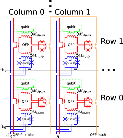
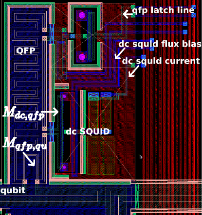
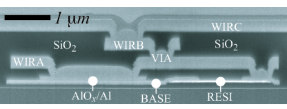
Figure 1 shows a high level schematic of a small portion of an XY-addressable readout system. Since this article is focused upon the readout architecture, we have suppressed the details of the flux qubits and their control circuitry and refer the reader to Refs. [7, 17] for information concerning those elements. Each qubit in the circuit requires two elements for readout: a dc SQUID and a QFP. Each dc SQUID has two shared control lines: a current bias (cb0, cb1, ) and a flux bias (fb0, fb1, ). All QFP latches share a single activation line (“QFP latch”, flux bias referred to as ) and a single flux bias line (“QFP flux bias”, flux bias referred to as ). Let the inductance and capacitance of the QFP be denoted by and , respectively. Each QFP is coupled to its affiliated qubit (dc SQUID) via a mutual inductance (). The top panel of figure 2 shows the physical layout of a portion of the readout system, as implemented in the chips discussed in this article. Note that the QFP is galvanically attached to the qubit; this is done purely to reduce the contribution of the readout to the length and inductance of the qubit. The bottom panel of this figure shows a cross-section of our planarized fabrication process that was used to produce the test circuits reported upon herein. All results presented in this article were obtained from test circuits containing either 8 or 128 flux qubits, as indicated in the text.
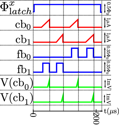
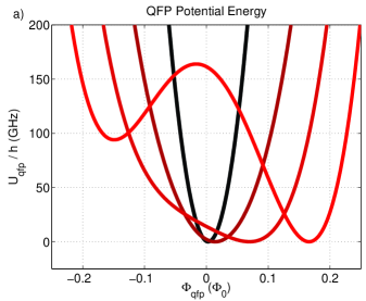
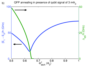
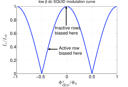
At a high level, the readout circuit functions as follows: During the course of an adiabatic quantum computation, all current biases and flux biases are set to zero, thus ensuring that the dc SQUIDs are in the zero voltage state. In order to decouple the QFPs from the flux qubits, the QFP latch line is set to provide to all QFPs, thus suppressing their persistent currents to negligible levels. Once the qubits have reached their final states at the end of an adiabatic quantum computation, the waveform sequence depicted in figure 3 is applied to the readout circuitry. First, the QFP latch bias is raised to provide to all QFPs, thus raising the QFP tunnel barriers (see figure 4), which adiabatically changes the state of each QFP from being the ground state of a monostable potential to being the groundstate of a bistable potential. The direction of the resultant groundstate persistent current flow about the body of each QFP is determined by the polarity of the flux imparted by the qubit to which each QFP is coupled. At the end of this linear ramp the height of the QFP tunnel barriers has been raised to a sufficiently high level so as to preclude further dynamics (, where is the temperature of the chip), and the final states of the flux qubits have been latched into the QFPs. Thereafter, a linear current ramp is applied to the bias cbx whose maximum amplitude is significantly lower than the maximum dc SQUID switching current amongst the population of dc SQUIDs connected in series with cbx, so that only the dc SQUID with a flux bias applied to its fby line is triggered (see figure 5). The timing of a voltage arising across the dc SQUID is then measured: If the flux arising from the QFP increases (decreases) the total flux applied to the dc SQUID addressed by cbx and fby, then switching to the voltage state will happen sooner (later) (see figure 3 and 7). This difference in timing reveals the state of the QFP and therefore the state of the qubit. A more detailed discussion of each of the elements in this readout architecture and their operation is presented below.
2.1 Qubit signal
For the purposes of reading the final state of the flux qubits in an AQO processor, the relevant signal is the magnitude of the qubit persistent current when the qubit tunnel barriers have been raised to their maxima. The flux qubits used in our circuits are of the type described in Ref. [7] and had inductances pH, of which pH was reserved for readout, and critical currents A. During readout, the qubit , corresponding to a circulating current of roughly . A typical mutual inductance from the qubit into its corresponding QFP is pH, leading to a qubit signal as seen by the QFP of m.
For the qubit parameters cited above, the maximum tunnel barrier height between flux states would be GHz. The design pressures that led to this choice are discussed in detail in [7, 17] and so we only briefly repeat the relevant points herein. While in theory one could design flux qubits with larger (and thus a larger to provide immunity to any dc SQUID driving signal) both asymmetry in the qubit junctions and finite precision on the qubit analog flux biases would eventually limit circuit performance as an AQO processor. Furthermore, typical AQO architectures require a substantial number of inter-qubit couplings [3] which necessitates larger than may be considered appropriate in the study of flux qubits for implementing GM hardware. As such, the flux qubits in our circuits tend to possess substantially smaller in order to realize appreciable single qubit tunneling energies over as broad of a range of annealing parameter as is practical. Consequently, our flux qubits appear to be more susceptible to resonant activation by dc SQUID switching transients than other flux qubits reported upon in the literature.
2.2 QFP latch
The QFP is a 2-junction rf SQUID, which, in comparison to our flux qubits [7], possesses a lower inductance pH and a substantially higher critical current A. Consequently, the former device has a maximum , a maximum persistent current A, and a maximum tunnel barrier between its two persistent current states on the order of THz (compare with 0.46 THz for the qubit). The effective 1-dimensional potential energy of a QFP with identical Josephson junctions can be written as
| (3) | |||||
where is the mean phase across the two Josephson junctions. Note that in tuning from to that morphs from being monostable to being bistable (see figure 4). Raising slowly adiabatically latches the state of each flux qubit into the QFP to which it is coupled. Adiabaticity is guaranteed here due to the large signal from the qubit and the relatively low bandwidth of the QFP latch line which has a rise time of approximately 1 . Adiabaticity is violated during the latching phase only if there is no signal applied to the QFP, as the two QFP circulating current states are then degenerate in energy in the large limit. Note that if the qubit state were to be unchanged after dc SQUID switching, then the QFP could be operated fully reversibly: the QFP could then be reset in the presence of the signal in which it was initially latched, so the whole cycle of barrier raising and lowering would then be adiabatic.
One challenge in designing QFPs (or any 2-junction rf SQUID) is that junction asymmetry leads to a -dependent effective flux offset [7]. This offset limits how small one can make , as one would like the bimodal qubit signal to straddle any such flux offset for values of about which the QFP becomes bistable. Assuming a typical fabrication spread of 1% in junction critical currents and a maximum , this offset could be up to m. For this reason, we had chosen such that m.
There are two other features of the QFP latch that make it useful beyond the qubit state readout method described thusfar. Linear detection: By biasing the QFP such that , it can be used as a preamplifier acting on the signal from the qubit. Realistically, achieving appreciable net flux gain into the dc SQUID requires careful tuning of the QFP and dc SQUID biases. Instead, to readily use the latching detector as a linear preamplifier, we apply flux feedback in software to the QFP body loop, to keep the QFP at its balance point where we have a 50% probability of measuring it in either of its persistent current states after latching. The required is then a linear representation of the signal from the qubit. At this balanced population point, the QFP has minimal back-action on the qubit and can be used to probe the magnitude of the circulating current of the qubit. We use this mode of operation of the QFP in order to calibrate qubit parameters, as described in [7]. Shift register readout: There is a well developed logic family based on QFPs [16], and it is straightforward to design a QFP-based shift register that terminates in a single dc SQUID. Such a readout architecture would require even fewer bias lines than our XY-addressable architecture. We have successfully fabricated and tested an 8-QFP-long shift register driven with a three phase clock as a prototype of such a readout scheme.
2.3 dc SQUID
The method for using a hysteretic dc SQUID for flux detection is discussed in [18] and more generally in [9, 10]. For the implementation discussed herein, current ramp times were typically and peak voltages from the dc SQUIDs after switching were typically kept to much less than the gap voltage of Nb to reduce heating on chip. The mutual inductance from the dc SQUID to the QFP was pH.
Basic operation of the XY-addressable array of dc SQUIDs is presented in figure 3. To read out the column and row QFP, we set the value of the current in the line in figure 1 to provide a flux bias of approximately 0.35 into the dc SQUIDs on that row and on all other rows. This results in the selective suppression of the critical current for only the dc SQUIDs in row to . Then, applying a current ramp on the column of maximum amplitude will cause the target dc SQUID to switch at a time that gives information about the flux coupled into dc SQUID from its QFP. In other words, the lines are used to row select by flux biasing all dc SQUIDs in the target row to a bias point where a current ramp on the dc SQUID will trigger readout (see figure 5). The lines are used as column selects and all other current biases are kept at zero. After we have registered an event, the current biases are reset to zero, and the process repeated for all combinations of and .
For devices with less than a few thousand qubits it is feasible to provide enough analog lines to run an XY-addressable readout scheme as described. Modifying this readout scheme by adding another control direction, for example an XYZ-addressable readout scheme where X and Z are summed together into the dc SQUID flux bias, changes the scaling of number of required wires to a cube root in the number of qubits, thereby allowing us practically scale up to reading tens of thousands of qubits. If margins on the XYZ-addressable scheme are too low, then we can implement the QFP shift register method described earlier which uses a constant number of analog lines. In that case we can use excess analog lines to decrease readout time or increase operating margins.
2.4 Electronics
The electronics to run the readout and qubit control were integrated into a compact rack system with 128 output channels, a fraction of which were devoted to readout. The dedicated readout channels had an amplifier, a tunable comparator chain and retriggerable timers in order to detect multiple SQUID switching events per channel. For the purposes of characterizing test circuits, we limited the readout sequence to a rate of approximately one dc SQUID switching event/100s per channel. Without modifying the line bandwidth (3 MHz), this could in principle be sped up to roughly one event/s. Further speed-up could be obtained by reading multiple columns simultaneously, but we have some experimental evidence that rf isolation between columns needs to be improved as dc SQUIDs from different columns can possibly interfere. With further work, one can likely reach the bandwidth limitation of the wiring in the refrigerator. For example, if a particular chip were to have 32 columns of dc SQUIDs and each line had a bandwidth of 3 MHz, one could obtain roughly a 50 Mbit/second readout rate.
2.5 Power consumption
The readout process dissipates energy onto the chip whenever a dc SQUID is in the voltage state. An upper bound on the total energy dissipated by the readout process can be estimated as follows: After the dc SQUID switches to the voltage state, the large capacitance of the refrigerator wiring and filtering () starts to charge with a rate set by , typically . For simplicity, we ignore the first several nanoseconds after switching which are dominated by transients and ringing as the lines are not matched to the high impedance the dc SQUIDs present upon switching. Until the dc SQUID reaches a significant fraction of the gap voltage there is little dissipation on chip. For fast operation we typically restrict the charging time to less than two to three microseconds to keep the dc SQUID from charging to the gap voltage and generating heat. For the data presented in this paper, though, we allowed many microseconds to pass (see figure 7). The resulting dissipated energy is . If we performed this same inefficient procedure with a readout cycle, we would obtain an average dissipated power during readout of , which would be well within the capabilities of a standard dilution refrigerator to dissipate.
3 Challenges
While we routinely fabricate and operate XY-addressable readout systems based upon the architecture described herein, there were some formidable challenges that had to be overcome in order to operate them to their full potential. While the typical challenges associated with proper design of cryostat wiring, filtering, and shielding were encountered, we focus here on only those issues directly related to the readout scheme.
First, challenges related to fabrication yields are typically soft failures where one loses either a row or a column or even a single readout element. Since the readout system discussed herein was typically a part of a large integrated circuit, it was possible to at least study large portions of a circuit even in the presence of a few fabrication errors.
Related to fabrication yield is the issue of critical current variation across a chip. For the dc SQUIDs, small variations of critical current are not a significant issue as there is plenty of range between OFF and ON switching currents in this XY-addressing scheme. The more frugal XYZ-addressable scheme described earlier, though, would come at the expense of a reduced ON and OFF switching current ratio in the presence of realistic critical current variations.
Similar to critical current variation, flux offsets of each dc SQUID lead to reduced ON/OFF margins as well. In practice, this proved to be the key challenge to operating large scale XY-addressable readout schemes in our laboratory. We now use a combination of passive magnetic shielding and active magnetic field compensation to achieve fields below 1 nT perpendicular to the chip. We still typically end up with flux offsets of a few m in QFPs and dc SQUIDs, which may be due to local magnetic impurities on the wiring or in the magnetic shielding. Cross-talk, both between off-chip and on-chip wiring, similarly reduces operating margins.
For the QFPs, asymmetry in the critical currents of their two Josephson junctions directly create an apparent flux offset that competes with the qubit signal, as discussed previously. Due to the threshold like latching, small differences in critical current do very little, while large differences render the device unusable as the qubit signal cannot overcome the asymmetry-induced flux bias acting on the QFP. Typical requirements are less than 2% junction critical current asymmetry in the QFP in order for the device to be operable.
A further subtle effect, which is relevant to fast operation of the readout circuit, is thermally induced hysteresis. If one tries to perform experiments with a fast repetition rate (for tuned dc SQUID ramps, this rate is typically 100 s), then the chip temperature is affected by dc SQUID heating (see discussion in §4 below). This dc SQUID heating depends quite strongly on when the dc SQUID escapes to the voltage state, and therefore what signal is applied to the dc SQUID. We have found that to measure any temperature dependent phenomena, such as the transition width of a QFP or qubit, where one simultaneously requires high speed and high accuracy measurements, we needed to temperature stabilize the mixing chamber of the dilution refrigerator at 35-40 mK (much above the 10 mK base temperature of the refrigerators) and take care to minimize the time the dc SQUID stays in the voltage state.
4 Readout errors
Our research has shown that there are two principle mechanisms response for imperfect readout in our XY-addressable readout. The first mechanism is the thermal noise on the QFP, and the second mechanism is the uncertainty in the switching time of the dc SQUID caused by the stochastic nature of the quantum tunneling from the zero voltage state to the voltage state[19]. Each of these error mechanisms will be discussed below.
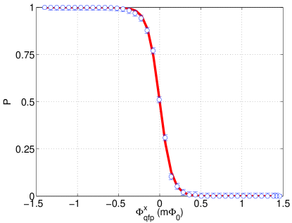
Examining the first error source, figure 6 shows the measured flux transfer curve of a typical QFP device, as obtained by latching the QFP state in the presence of a constant flux through the QFP flux bias line. The data represent the probability of observing one of the QFP persistent current states versus . Note that the data yield a smoothed step function with a width . This finite width is due to imperfect initialization of the QFP state.
To understand the source of this QFP transition width, it suffices to analyze the dynamics of the two lowest QFP energy levels as the barrier between flux states is raised (as in figure 4) in the presence of a thermal bath. As the barrier is raised, the tunneling energy between localized flux states is reduced to zero. Once is high enough and low enough the system is no longer able to maintain a state that is in thermal equilibrium. We estimate this dynamical freeze-out to occur when MHz, given our QFP annealing times (time taken to raise the QFP barrier) of roughly 1 s. The dynamics of the QFP as approaches this small value are well described by the incoherent tunneling picture studied in Refs. [20, 21]. The value of the QFP persistent current, calculated from extracted device parameters at that point, is A. We can then convert the abscissa in figure 6 from flux to energy (2 ). By fitting the QFP population as a function of to the expected functional form in the limit ,
| (4) |
we extract an effective mK for the QFP and its local bath. For comparison, the refrigerator was stabilized at approximately 40 mK. If we decrease the cooling time after the dc SQUID switching event before the QFP latch in the next measurement frame we can characterize the cooling of the QFP after the dc SQUID heating event:
| Cooling time (s) | Temperature (mK) |
|---|---|
| 300 | |
| 1000 | |
| 2000 | |
| 4000 |
When operated with dc SQUID current biases tuned to minimize heating, or with sufficient cooling time such as the effective 47 mK data shown in figure 6, we obtain a corresponding flux sensitivity of the QFP of . For comparison, the qubit signal coupled into the QFP is of order 10 m. This results in practically zero error probability for the latch.
The QFP flux uncertainty (142 ) is significantly better than that of its accompanying dc SQUID, which was estimated to be 1.8 m from the width of its switching distribution. This dramatic difference in sensitivity arises from the fact that dc SQUID noise results from the stochastic nature of quantum tunneling from the zero voltage to finite voltage state with an equivalent temperature of several hundred mK, while the QFP annealing step leads to a thermal uncertainty near the refrigerator temperature of 40 mK.
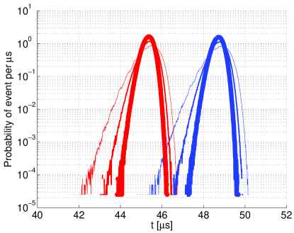
Focusing now on the second error mechanism, figure 7 shows measured switching histograms of a single dc SQUID for the case when its respective qubit is first initialized in one state (red) and then in the other (blue). While the dc SQUID switching distributions are characteristic of quantum tunneling and thus asymmetric, we still can characterize the dc SQUID sensitivity by the standard deviation of the switching histogram. The abscissa can be converted from time to flux by direct measurement of the shift in switching time as a known amount of flux is applied to the dc SQUID. The resulting dc SQUID sensitivity is 1.8 m per read, and the signal from the QFP latch is 11.9 m, resulting in a measured error probability of the dc SQUID in reading the QFP as small as 0.01. This is a reasonably low error probability, but we require even lower error rates in order to implement a large scale AQO processor. It is trivial to decrease this dc SQUID limited error by taking more samples of the dc SQUID switching time since the QFP maintains its state between these samples. The results of this repeated reading of the dc SQUID on its resolving power are shown in figure 7. After 2 reads, the dc SQUID sensitivity increases to 1.3 m and after 4 reads to 0.9 m. At 4 reads we obtain an error probability of . This error probability includes qubit initialization errors, QFP errors, and dc SQUID errors. This behaviour, while varying slightly quantitatively, was similar for all 8 readouts on the particular test chip used to generate these data.
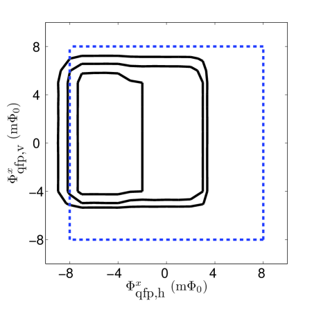
To demonstrate the performance of a large-scale XY-addressable readout system, we present the results of a system level margin measurement from a 128-qubit chip in figure 8. This particular chip had two flux biases to provide to the 128 QFPs: The two lines each biased 64 QFPs, with the two groups partitioned depending upon the physical orientation of the QFP body and denoted as “horizontal” or “vertical”. The reader is referred to [6] for a description of the 128-qubit chip physical layout. We then studied the error probability of the readout system as a function of horizontal and vertical QFP biases. In order to render the readout test independent of the details of quantum annealing, we prepared the 128 qubits into a known state by setting all of the inter-qubit couplings to zero [18], biasing all qubits using their local flux sources [17] hard to one side, and then raising their tunnel barriers. This placed each flux qubit into a known state with certainty. We then read the state of each qubit, as described above using a single dc SQUID switching measurement. This sequence was repeated 128 times for every point on a 2-dimensional grid in -space. The resultant contours of constant error are shown in figure 8 as black lines, as well as the designed margins as a blue dashed line. Inside the 1 error contour we observed no errors out of 128 reads of the entire 128 qubit system. These measurements alone confirm that the system level error rate can be less than when appropriately biased. The offset of the measured margins in the horizontal direction was due to a single QFP with a flux offset, either from Josephson junction asymmetry or flux pinning, of m. When this particular readout failed due to the inability of the qubit signal to straddle that QFP’s degeneracy point, it contributed 1/128 to the total failure rate, thus dominating the shape of the inner most contour. The next margin contour then required a much larger horizontal flux bias shift to cause a second QFP to fail repeatedly. The slow increase in failure rates is due to a several m random distribution of flux offsets in the QFPs.
In order to better quantify the performance of the 128 qubit readout system, we biased the QFPs to an operating point near the center of the margin plot, m, and performed 65536 measurements in the manner cited above. We observed 5 errors out of 65536 measurements, which then provided an estimated system level error probability of . The five errors were attributed to different readouts and were probably due to the stochastic nature of the dc SQUID switching. From these results, we can crudely estimate the per qubit error to be on the order of for the 128 qubit chip. This could be improved upon by simply using repeated dc SQUID reads, as was done with the 8 qubit chip, and the final limit upon the readout error probability will likely be determined by outlier events not captured in the preceding discussions.
5 Conclusions
We have described and implemented a scalable XY-addressable readout scheme that is suitable for a superconducting adiabatic quantum optimization system and measured the readout error rate and margins of an 8- and 128-qubit system, respectively. We conclude that the single qubit readout error rate can be made less than using the QFP enabled architecture, which makes readout errors a non-issue for large scale integrated circuits of the types considered herein. We have experimentally demonstrated a system level error rate of using a 128 qubit circuit. We do not expect any significant challenges in further scaling this architecture to about one thousand qubits. Finally, we have briefly discussed both an XYZ-addressable and a QFP shift register based solution that would facilitate scaling up to read even larger numbers of qubits on a single chip.
Acknowledgments
The authors would like to thank F. Brito, B. Bumble, D. Bruce, E. Chapple, P. Chavez, V. Choi, F. Ciota, C. Enderud, A. K. Fung, S. Govorkov, S. Han, J. P. Hilton, A. Kaul, A. Kleinsasser, D. Klitz, G. Lamont, P. Lumsden, F. Maibaum, R. Neufeld, T. Oh. L. Paulson, I. Perminov, C. Petroff, D. Pires, C. Rich, P. Spear, A. Tcacuic, M. Thom, S. Uchaikin, M. Wang, and A. B. Wilson for work on cryogenics, electronics, fabrication, filtering, and magnetic shielding.
References
References
- [1] M. F. Bocko, A. M. Herr, and M. J. Feldman. Prospects for quantum coherent computation using superconducting electronics. IEEE Trans. Appl. Supr., Jun 1997.
- [2] Michel H. Devoret and John M. Martinis. Implementing qubits with superconducting integrated circuits. Quantum Information Processing, 3(1-5):163–203, 2004.
- [3] W. M. Kaminsky and S. Lloyd. Scalable architecture for adiabatic quantum computing of np-hard problems. In Quantum Computing and Quantum Bits in Mesoscopic Systems. MQC2, Kluwer Academic, 2003.
- [4] E. Farhi, J. Goldstone, S. Gutmann, and M. Sipser. A quantum adiabatic evolution algorithm applied to random instances of an np-complete problem. Science, 292(5516):472–475, April 20 2000.
- [5] M. Grajcar, A. Izmalkov, and E. Il’ichev. Possible implementation of adiabatic quantum algorithm with superconducting flux qubits. Phys. Rev. B, 71(14):144501, Apr 2005.
- [6] R. Harris, M. W. Johnson, T. Lanting, A. J. Berkley, J. Johansson, P. Bunyk, E. Tolkacheva, E. Ladizinsky, N. Ladizinsky, T. Oh, F. Cioata, I. Perminov, P. Spear, C. Enderud, C. Rich, S. Uchaikin, M. C. Thom, E. M. Chapple, J. Wang, B. Wilson, M. H. S. Amin, N. Dickson, K. Karimi, B. Macready, C. J. S. Truncik, and G. Rose. Experimental investigation of an eight-qubit unit cell in a superconducting optimization processor. Phys. Rev. B, 82(2):024511, Jul 2010.
- [7] R. Harris, J. Johansson, A. J. Berkley, M. W. Johnson, T. Lanting, Siyuan Han, P. Bunyk, E. Ladizinsky, T. Oh, I. Perminov, E. Tolkacheva, S. Uchaikin, E. M. Chapple, C. Enderud, C. Rich, M. Thom, J. Wang, B. Wilson, and G. Rose. Experimental demonstration of a robust and scalable flux qubit. Phys. Rev. B, 81(13):134510, Apr 2010.
- [8] R. Harris, T. Lanting, A. J. Berkley, J. Johansson, M. W. Johnson, P. Bunyk, E. Ladizinsky, N. Ladizinsky, T. Oh, and S. Han. Compound josephson-junction coupler for flux qubits with minimal crosstalk. Phys. Rev. B, 80(5):052506, Aug 2009.
- [9] C. Cosmelli, P. Carelli, M. G. Castellano, F. Chiarello, R. Leoni, and G. Torrioli. A hysteretic dc squid reading the flux states of an rf squid. IEEE Trans. Appl. Supr., 11(1):990–993, Mar 2001.
- [10] M. G. Castellano, F. Chiarello, R. Leoni, D. Simeone, G. Torrioli, C. Cosmelli, R. Buttiglione, S. Poletto, and P. Carelli. Tracing the characteristics of a flux qubit with a hysteretic dc-superconducting quantum interference device comparator. Journal of Applied Physics, 94(12):7935–7937, 2003.
- [11] I. Chiorescu, Y. Nakamura, C.J.P.M. Harmans, and J.E. Mooij. Coherent quantum dynamics of a superconducting flux qubit. Science, 299:1869–1871, 2003.
- [12] M. Grajcar, A. Izmalkov, E. Il’ichev, Th. Wagner, N. Oukhanski, U. Hübner, T. May, I. Zhilyaev, H. E. Hoenig, Ya. S. Greenberg, V. I. Shnyrkov, D. Born, W. Krech, H.-G. Meyer, Alec Maassen van den Brink, and M. H. S. Amin. Low-frequency measurement of the tunneling amplitude in a flux qubit. Phys. Rev. B, 69(6):060501, Feb 2004.
- [13] A. Lupaşcu, E. F. C. Driessen, L. Roschier, C. J. P. M. Harmans, and J. E. Mooij. High-contrast dispersive readout of a superconducting flux qubit using a nonlinear resonator. Physical Review Letters, 96(12):127003, 2006.
- [14] J. R. Friedman, V. Patel, W. Chen, S. K. Tolpygo, and J.E. Lukens. Quantum superposition of distinct macroscopic states. Nature, 406:43–46, 2000.
- [15] K. K. Likharev et al. Reversible conveyor computation in an array of parametric quantrons. IEEE Trans. Mag., page 947, 1985.
- [16] W. Hioe and E. Goto. Quantum flux parametron: a single quantum flux superconducting logic device (Studies in Josephson supercomputers) (v. 2). World Scientific, Feb 1991.
- [17] M W Johnson, P Bunyk, F Maibaum, E Tolkacheva, A J Berkley, E M Chapple, R Harris, J Johansson, T Lanting, I Perminov, E Ladizinsky, T Oh, and G Rose. A scalable control system for a superconducting adiabatic quantum optimization processor. Superconductor Science and Technology, 23(6):065004, 2010.
- [18] R. Harris, A. J. Berkley, M. W. Johnson, P. Bunyk, S. Govorkov, M. C. Thom, S. Uchaikin, A. B. Wilson, J. Chung, E. Holtham, J. D. Biamonte, A. Yu. Smirnov, M. H. S. Amin, and Alec Maassen van den Brink. Sign- and magnitude-tunable coupler for superconducting flux qubits. Physical Review Letters, 98(17):177001, 2007.
- [19] R. F. Voss and R. A. Webb. Macroscopic quantum tunneling in 1-m nb josephson junctions. Phys. Rev. Lett., 47:265–268, July 1981.
- [20] M. H. S. Amin and Dmitri V. Averin. Macroscopic resonant tunneling in the presence of low frequency noise. Physical Review Letters, 100(19):197001, 2008.
- [21] R. Harris, M. W. Johnson, S. Han, A. J. Berkley, J. Johansson, P. Bunyk, E. Ladizinsky, S. Govorkov, M. C. Thom, S. Uchaikin, B. Bumble, A. Fung, A. Kaul, A. Kleinsasser, M. H. S. Amin, and D. V. Averin. Probing noise in flux qubits via macroscopic resonant tunneling. Physical Review Letters, 101(11):117003, 2008.