Characterisation of radiation damage in silicon photomultipliers with a Monte Carlo model
Abstract
Measured response functions and low photon yield spectra of silicon photomultipliers (SiPM) were compared to multi-photoelectron pulse-height distributions generated by a Monte Carlo model. Characteristic parameters for SiPM were derived. The devices were irradiated with 14 MeV electrons at the Mainz microtron MAMI. It is shown that the first noticeable damage consists of an increase in the rate of dark pulses and the loss of uniformity in the pixel gains. Higher radiation doses reduced also the photon detection efficiency. The results are especially relevant for applications of SiPM in fibre detectors at high luminosity experiments.
keywords:
Silicon photomultiplier , Monte Carlo model for detector output , single-electron response function , radiation damagePACS:
29.40.Wk , 85.60.Bt , 61.80.Fe, , and
1 Introduction
After a few years of R&D, silicon photomultipliers (SiPM) are today an interesting alternative to conventional vacuum phototubes in many applications due to the specific advantages of a solid state device: small size, low voltage operation and magnetic field insensitivity Buzhan2001 ; Dolgoshein ; Dolgoshein-2006 . Nevertheless, the idea of grouping hundreds of miniature avalanche photodiodes (APD) in a planar array to form an analog device has found a limitation in the high rate of intrinsic dark pulses of such a configuration. Only small active area devices are currently available and typical noise rates are of the order MHzmm2 with signal pile-up due to optical cross-talk. This leads to the situation of a small photo-sensor that needs to detect a relatively large amount of light in order to achieve an acceptable signal-to-noise ratio. To our knowledge there has been no attempt to use SiPM in applications where only a few photons must be detected. This is for example the situation faced when using scintillating fibres as tracking detectors.
There is little information about radiation hardness of SiPM. It is well known from other types of silicon detectors that generating centres are created during irradiation which increase the leakage current Leroy . The bulk leakage current is multiplied in APD by the gain factor and the resulting pulses are undistinguishable from photon generated events. Consequently, an increasing rate of dark pulses as a function of the radiation dose is expected for SiPM. Low light level detection will be degraded or even impossible in some applications if this effect happens to be large. Adverse effects of irradiation on other characteristic parameters of SiPM such as gain uniformity, after-pulsing or optical cross-talk probability will be also detrimental for a detector. In general, it is mandatory to study the impact of the particular kind of radiation the detector will be exposed to on the characteristic parameters that must remain stable.
In this paper a complete model for multi-photoelectron pulse-height distributions (MPHD) was used to extract the main consequences of electromagnetic irradiation on SiPM. Section 2 discusses the MPHD model. Section 3 gives a brief description of the irradiation set-up. Section 4 describes the changes in SiPM characteristics obtained for low and high irradiation doses. Section 5 closes with future prospects of using this kind of detectors in low light level applications.
2 The Monte Carlo model for the detector output
A complete model for the MPHD of SiPM was derived based on a Monte Carlo simulation. For the model, Poisson distributed photo-electron and dark signals are generated independently. Each of these signals can cause optical cross-talk and after-pulses according to a given probability distribution. For this set of pixels the distribution in time is generated with respect to an integration time window. Single pixels can contribute with varying gain to the generation of the detector output. Finally, the noise is added. The free parameters of the simulation are: mean signal amplitude (), gain variation (), dark pulse rate (), optical cross-talk probability (), after-pulse probability (), trap lifetime (), mean number of detected photons (), pedestal position (), and noise amplitude (). In the following, the simulated processes are explained.
As SiPM are a set of APD connected in parallel many of their properties are thus inherited. Its dark count rate, , is the sum of all the APD dark count rates. After-pulses appear in each pixel after a photon (or a thermically generated charge carrier) triggers an avalanche due to trapped carriers that are released after some time-delay. The after-pulse probability, , is defined as the fraction of events in which one additional signal is generated after the detection of a photon. It is the product of the trapping probability and the triggering probability, both increasing linearly with the applied bias voltage. The trap lifetime, , determines the typical time-scale.
SiPM are manufactured so that signal uniformity from pixel to pixel is quite good, typically within 10 % Renker . The small variation, , together with the narrow single electron response function of each APD provides excellent photon counting capabilities and as many as 20 photons can easily be resolved in a typical pulse height spectrum Buzhan2001 . The distance between multi-pixel peaks in the spectrum is a measure of the charge gain, .
Surface leakage currents do not cross the multiplication region. Their fluctuations are merged with other noise sources to define the noise amplitude as measured by the pedestal width, . A change in the surface leakage current should also appear as a shift in pedestal position, .
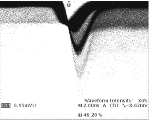
An avalanche of carriers in any of the micro-metric APD forming the SiPM will create around 50 photons via hot carrier luminescence with enough energy to trigger any neighbouring pixel Otte . Devices without trenches filled with opaque material exhibit optical cross-talk, where at least one photon is able to cross the spacing between micro-cells to produce a simultaneous signal (within 100 ps). Fig. 1 shows the effect of optical cross-talk in the SiPM elementary signal. The well defined amplitudes of the multi-pixel events is a result of the simultaneity of the composing signals.
To the knowledge of the authors there has been only one serious attempt to describe the statistics of multi-photoelectron pulse-height distributions Wright . A.G. Wright points out that the combination of the Poissonian nature of most light sources and the Binomial character of the photoelectric effect will give rise to a Poisson distribution for the number of detected photons. He goes on by establishing a method that uses this fact in an efficient way to build up the full pulse-height spectrum by using the response function of the corresponding detector. This method faces the fact that in many cases the response to a single photon is far from being Gaussian. Experimental input is used to accurately describe the amplitude distribution with no ad hoc assumption about how the detector will react to a single photon.

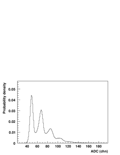
In our MPHD model the violation of Poissonian statistics arises from the well known SiPM characteristics, incorporating the multiple-peak structure. It also makes use of the simplifying assumption that the individual peaks in the response function are Gaussian distributed. It was observed that when bias voltages are low and pixels are assumed to behave in a practically independent way, the Gaussian hypothesis reproduces with great accuracy the measured spectra. Fig. 2(a) shows the measured response function of a Photonique device111SSPM-0701BG-TO18 by Photonique SA, http://www.photonique.ch (2007) for a bias voltage of 17.5 V after irradiation with a fluence of electrons of 14 MeV energy. Fig. 2(b) shows the result of a random integration of noise signals for the same gate width. The relatively large number of counts outside the pedestal peak is a result of the high rate, , of dark pulses. A simple convolution would add those events several times. SiPM are evolving toward the situation in which this algorithm can be successfully applied. Nowadays, devices are unfortunately not perfect and the high noise rate, for instance, would make the method inoperative.

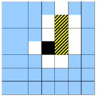

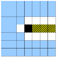
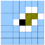
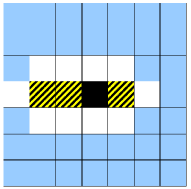
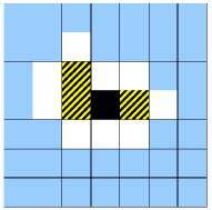
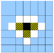
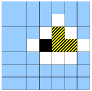
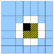

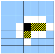
Optical cross-talk is modeled by considering the probability, , of simultaneous activation of two isolated pixels when one of them has been triggered and deducing the probability for all possible clusters in the SiPM pixel matrix. No distinction is made when there is more than one neighbour active. Fig. 3 shows all independent cluster types for the case of three additional pixels. Only pixels sharing one side are allowed as part of a cluster. Cluster probabilities are given by the zero pixel cross-talk probability , and the -pixel cross-talk probabilities , , and . The terms with are a consequence of the requirement that the pixels outside the cluster have to remain off. In absence of optical cross-talk, noise and after-pulses the pixel number distribution should be Poissonian. The mean value of this distribution, , gives a measure of the photon detection efficiency.
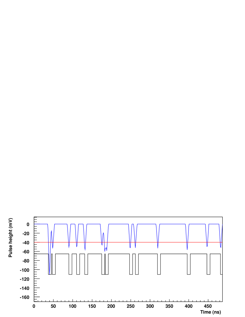
A realistic leading edge discriminator was implemented taking into account the blocking time of the module while the output is active (10 ns). Fig. 4 shows some of the pulses generated by the MPHD model, the threshold line and the output of the leading edge discriminator. Superposition of signals and optical cross-talk are visible in the first two peaks, a variation in amplitude can be observed in the next three single pixel signals and an after-pulse is visible in the next group of piled-up signals.
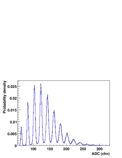
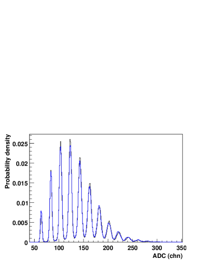
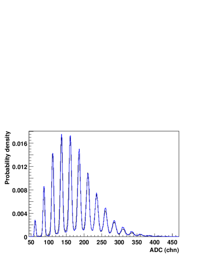
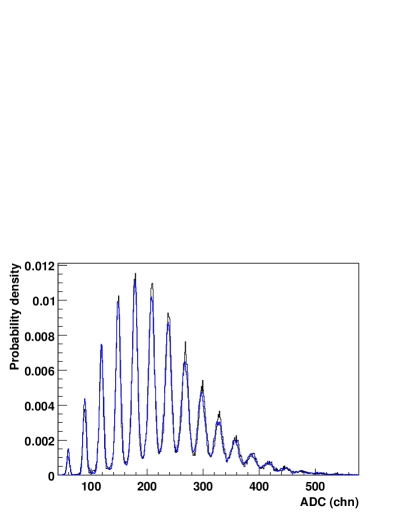
| parameter | 17.0 V | 17.4 V | 17.9 V | 18.4 V | 18.9 V |
|---|---|---|---|---|---|
| (mV) | 35. | 43. | 55. | 66. | 78. |
| (chn) | 0.08 | 0.07 | 0.05 | 0.07 | 0.06 |
| (MHz) | 3.21 | 4.06 | 4.50 | 6.35 | 7.33 |
| 0.011 | 0.020 | 0.028 | 0.033 | 0.048 | |
| 0.02 | 0.08 | 0.10 | 0.13 | 0.17 | |
| (ns) | 8.1 | 8.0 | 9.6 | 8.6 | 11.9 |
| (ph.) | 2.76 | 3.27 | 3.99 | 4.60 | 5.06 |
| (chn) | 65.2 | 63.9 | 61.6 | 59.0 | 54.9 |
| (chn) | 1.49 | 1.69 | 2.10 | 2.45 | 3.40 |

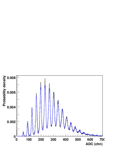
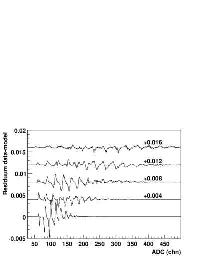
Fig. 5 shows the measured pulse-height spectra for low amplitude signals induced by a short pulsed UV laser222NanoLED by Horiba Jobin Yvon, http://www.jobinyvon.com/NanoLED (2007) exciting a plastic scintillator. The data was taken with five different bias voltages. Underlying curves are the results of the MPHD model. The residuum between MPHD model and data is shown in panel (f), where the curves for difference bias voltages are off-set by 0.004 to improve visibility. Table 1 summarises the resulting set of parameters. Fig. 6 shows the measured noise rate for a bias voltage of 17.9 V. The step structure is due to the multi-pixel events caused by optical cross-talk. Its sharpness is governed by the gain uniformity over the pixels and by the narrowness of the single pixel response function. Last steps are less defined due to the higher number of pixels involved. The pixels are better resolved with increasing bias voltages as a result of well known increase in the charge gain. The strong increase of noise rate with bias voltage is also visible. The open symbols are a result of the Monte Carlo. Simulated noise amplitude and gain variation have the same value as given in Table 1.
3 SiPM irradiation
A large increase of dark rate has been reported for relatively small radiation doses Musienko . After irradiation the noise rate increases because of the introduction of generation centers. This is the same behavior as for the bulk leakage current in diodes. In addition the creation of trapping centers is expected to increase the after-pulse probability. The application of the MPHD model described in the last section for the extraction of the characteristic parameters is considerably simpler when the multi-photoelectron peak structure is easily distinguishable. On the other hand the complete loss of this peak structure defines the limit of the application of SiPM for low light levels detection. The first irradiation dose was chosen so that only a small distortion of the peak structure was obtained. 14 MeV electrons were used to irradiate a sample of SSPM-0701BG-TO18 diodes. The beam current was 10 nA. The electrons crossed a 0.3 mm thick aluminum window at 15 cm distance from the 1 mm2 active area of the SiPM. Fluences on the diodes ranged from to electronsmm2. Heat dissipation and damage on the transparent epoxy layer protecting the silicon material were calculated and proved to be negligible. Grounding of the diode was provided in order to avoid damage by the sudden release of accumulated charge.
4 Characterisation of the irradiation damage
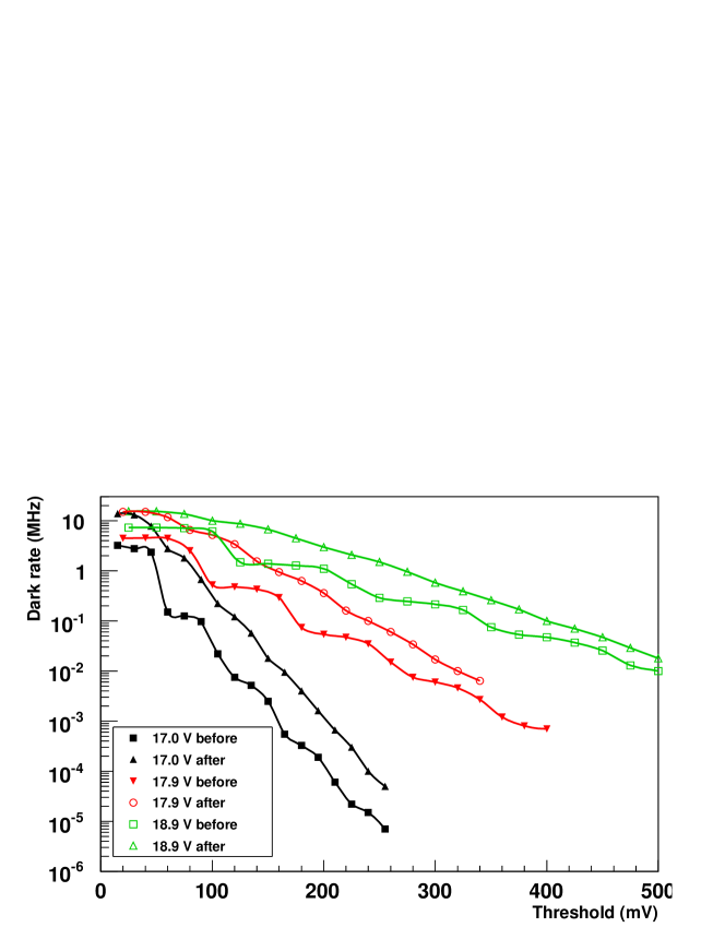
The SiPM were characterised before and after irradiation by studying the noise rates and the pulse-height spectra for low amplitude signals. Fig. 7 shows the noise rate before and after irradiation with electrons of 14 MeV energy as a function of threshold in a leading edge discriminator. The figure includes curves for three different bias voltages. Two observations were made after the irradiation:
-
1.
the rates of dark pulses are significantly larger.
-
2.
the steps are much less pronounced than before irradiation.
The simulation shows that an increase in the dark count rate is insufficient to explain the curves and it confirms that either an increase in the noise amplitude or the loss of gain uniformity (or a combination of both) can reproduce the measured values.
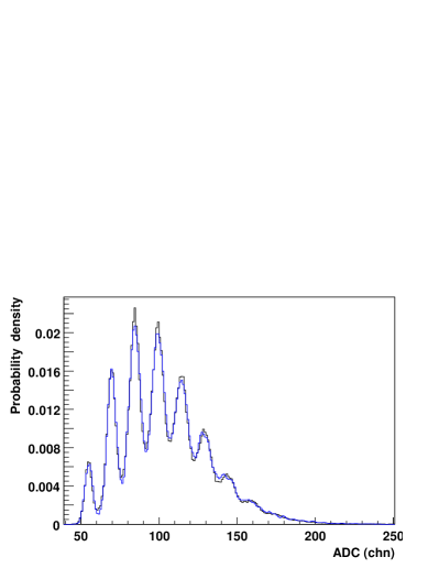
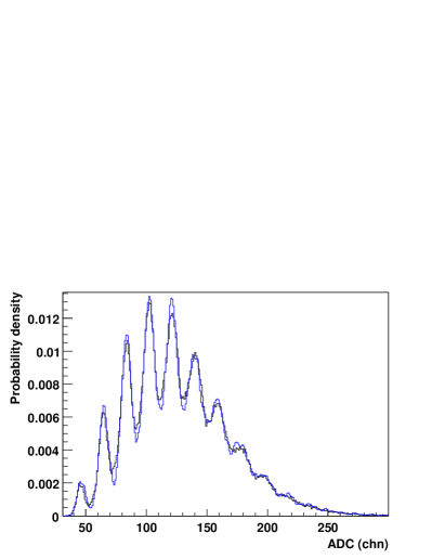
The histograms in Fig. 8 show measured ADC spectra for bias voltages of 17.0 and 17.4 V (compared to 17.9 V recommended voltage). The MPHD model was tested on this low photon yield data. The simulated integration of signals was performed in an interval of 30 ns, and the mean width of the single-pixel signal was 9 ns. The pedestal peak in this case was clearly separated from the one-pixel peak. After-pulse probability was set to zero and the values for the noise rate and optical cross-talk probability were deduced from the measured noise rates as a function of discriminator threshold. The value of was given to a good approximation by the ratio of noise rates above and below the first step . The dark count rate might naively be taken from the measurement at lowest discriminator threshold, however, this value is not reliable due to the high probability of signal pile-up. If one assumes that the optical cross-talk probablility was not significantly modified by the low radiation doses the dark count rate can be calculated by multiplying the noise rate for a threshold between one and two pixels by . The distributions were well reproduced when noise amplitude and gain variation were allowed to change. The values for the gain variation before and after irradiation were 0.08 chn and 0.12 chn, respectively. The noise amplitude changed from 1.49 chn before to 2.44 chn after irradiation. The good matching of the two curves is a confirmation of the hypothesis of low after-pulse probability. It seems necessary to conclude that there has been an increase in leakage current and a severe loss of gain uniformity.
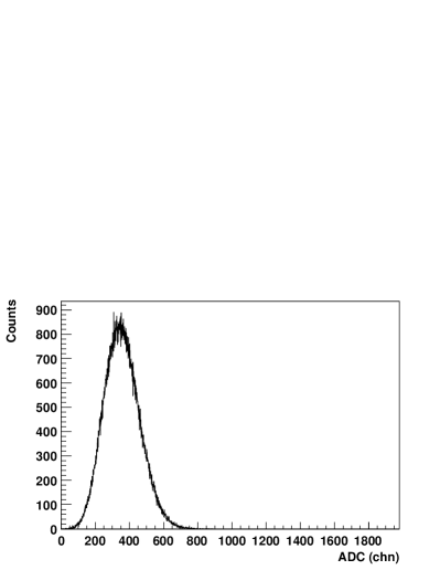
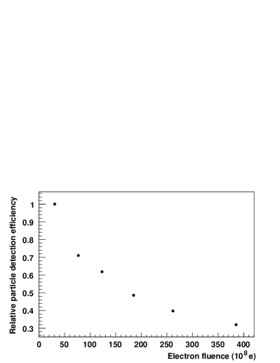
For higher fluences the noise increase is so large that a multi-photoelectron peak differentiation is no longer possible. A different approach was used for dealing with such a situation: noise should not be relevant for large signals but a variation in the gain or photon detection efficiency should still be noticeable by studying the position of the maximum in the pulse-height spectrum, see Fig. 9 (a). The result of such an investigation is shown in Fig. 9 (b). The single pixel signal was monitored after each irradiation and no change in its amplitude was observable. The conclusion has to be that there has been a progressive reduction of the photon detection efficiency. This fact can be attributed to the loss of a progressively larger amount of pixels which remain permanently in the off state or to the reduction in the photon detection efficiency of each pixel. Any of these two effects would be equally problematic for low light level detection.
5 Conclusions
Multi-anode photomultipliers are routinely used for scintillating fibre detector read-out showing all the drawbacks of conventional phototubes: stiff cables, high voltage power supplies and magnetic field sensitivity in addition to the specific problem of optical cross-talk among their many channels. If SiPM could be used instead an overall price reduction and a considerable detector simplification would be obtained. Conventional experimental techniques used to deal with high noise rates such as coincidences of several detectors can be complemented with more sophisticated methods based on intelligent trigger algorithms implemented in FPGA chips in order to obtain a reliable tracking detector. Cooling Peltier modules would reduce dramatically the noise rates in case the mentioned methods prove to be insufficient Eraerds .
For the KaosA1 spectrometer at the Mainz Microtron, Germany, the viability of a fiber detector is studied as part of the electron arm tracking system in which SiPM are considered as possible photon detectors Achenbach-SNIC06 . Simultaneously, a scintillating fibre tracker with SiPM read-out is being considered for the time-of-flight start detector or for a secondary active target in the future ANDA experiment PANDA at FAIR. Here, radiation hardness is an important issue due to the relatively small distance from the target area to the detector position.
A fluence of only particles reduces already the number of detected photons by a factor of two. Good shielding will be necessary in many applications where these doses are accumulated in a relatively short time.
Acknowledgements
We thank the MAMI accelerator staff for their help in the SiPM irradiations. Work supported in part by the European Community under the “Structuring the European Research Area” Specific Programme as Design Study DIRACsecondary-Beams (contract number 515873).
References
- [1] P. Buzhan, B. Dolgoshein, A. Ilyin, V. Kantserov, V. Kaplin, A. Karakash, A. Pleshko, E. Popova, S. Smirnov, Y. Volkov, L. Filitov, S. Klemin, F. Kayumov, An advanced study of silicon photomultiplier, ICFA Instr. Bull. 23 (2001) 28–41.
- [2] B. Dolgoshein, Silicon photomultipliers in particle physics: Possibilities and limitations, in: Proceedings of the 42nd Workshop on Innovative Detectors for Supercolliders, Erice, Italy, 28 September – 4 October 2003, World Scientific, Singapore, 2004, pp. 442–456.
- [3] B. Dolgoshein, V. Balagura, P. Buzhan, M. Danilov, L. Filatov, E. Garutti, M. Groll, A. Ilyin, V. Kantserov, V. Kaplin, A. Karakash, F. Kayumov, S. Klemin, V. Korbel, H. Meyer, R. Mizuk, V. Morgunov, E. Novikov, P. Pakhlov, E. Popova, V. Rusinov, F. Sefkow, E. Tarkovsky, I. Tikhomirov, Calice/SiPM Collaboration, Status report on silicon photomultiplier development and its applications, Nucl. Instr. and Meth. A 563 (2006) 368–376.
- [4] C. Leroy, P.-G. Rancoita, Particle interaction and displacement damage in silicon devices operated in radiation environments, Rep. Prog. Phys 70 (2007) 493–625.
- [5] D. Renker, Geiger-mode avalanche photodiodes, history, properties and problems, Nucl. Instr. and Meth. A 567 (2006) 48–56.
- [6] N. Otte, The silicon photomultiplier – a new device for high energy physics, astroparticle physics, industrial and medical applications, in: V. Luth (Ed.), Proceedings of the IX International Symposium on Detectors for Particle, Astroparticle and Synchrotron Radiation Experiments, SLAC, 3–6 April 2006, eConf C0604032, 2006, p. 18.
- [7] A. Wright, The statistics of multi-photoelectron pulse-height distributions, Nucl. Instr. and Meth. A 579 (2007) 967–972.
- [8] Y. Musienko, D. Renker, S. Reucroft, R. Scheuermann, A. Stoykov, J. Swain, Radiation damage studies of multipixel geiger-mode avalanche photodiodes, Nucl. Instr. and Meth. A 581 (2007) 433–437.
- [9] P. Eraerds, M. Legré, A. Rochas, H. Zbinden, N. Gisin, SiPM for fast photon-counting and multiphoton detection, Opt. Express 15 (22) (2007) 14539–14549.
- [10] P. Achenbach, et al., New detectors for the kaon and hypernuclear experiments with KAOS at MAMI and with PANDA at GSI, in: V. Luth (Ed.), Proceedings of the IX International Symposium on Detectors for Particle, Astroparticle and Synchrotron Radiation Experiments, SLAC, 3–6 April 2006, eConf C0604032, 2006, p. 144.
- [11] ANDA Collabaration, Strong interaction studies with antiprotons, Technical Progress Report, GSI, Darmstadt (2005).