Limit to 2D mobility in modulation-doped GaAs quantum structures: How to achieve a mobility of 100 millions
Abstract
Considering scattering by unintentional background charged impurities and by charged dopants in the modulation doping layer as well as by GaAs acoustic phonons, we theoretically consider the practical intrinsic (phonons) and extrinsic (background and dopants) limits to carrier mobility in modulation doped AlGaAs-GaAs 2D semiconductor structures. We find that reducing background impurity density to cm-3 along with a modulation doping separation of 1000 Å or above will achieve a mobility of cm2/Vs at a carrier density of cm-2 for K. At (10)K, however, the hard limit to the 2D mobility would be set by acoustic phonon scattering with the maximum intrinsic mobility being no higher than 22 cm2/Vs. Detailed numerical results are presented as a function of carrier density, modulation doping distance, and temperature to provide a quantitative guide to experimental efforts for achieving ultra-high 2D mobilities.
pacs:
73.40.-c, 73.21.Ac, 71.30.+hOne of the most spectacular achievements of modern materials science is the continued enhancement of low temperature (K) 2D electron mobilities in confined GaAs structures (e.g. quantum wells, heterostructures) over the last 30 years stormer ; pfeiffer ; heiblum . In particular, the invention of modulation doping technique stormer allowing spatial separation between dopants and carriers in 2D semiconductor quantum structures and the continuous improvement in molecular beam epitaxy (MBE) eliminating unintentional charged impurities from the background have led to an exponential increase in the low-temperature 2D carrier mobility in modulation doped GaAs-AlGaAs quantum structures from roughly cm2/Vs in 1977stormer to cm2/Vs in 2007heiblum , an amazing increase of mobility by a factor of 7000 in 30 years. Although much less widely known than Moore’s law, this is roughly equivalent to a factor of 3 increase in effective carrier velocity for every three years, more or less the same exponential rate of increase as in the celebrated Moore’s law for Si microprocessors except that instead of miniaturization, which drives the Moore’s law in Si electronics, modulation doping directly enhances the low temperature carrier mobility. This astonishing 7000-fold low-temperature mobility enhancement in GaAs based 2D systems has been possible entirely through the systematic suppression of charged impurity scattering and interface roughness scattering in GaAs-AlGaAs heterostructures and AlGaAs-GaAs-AlGaAs quantum wells (which can be thought of as double heterostructures). This exponential increases in 2D mobility is therefore a triumph of materials science, not lithographic processing. The primary motivation for enhancing 2D mobility comes from the physics of fractional quantum Hall effect (FQHE) where higher mobility leads invariably to the discovery of new phenomena Dean . Recent theoretical developments dassarma on topological quantum computation have provided added impetus heiblum to increasing 2D mobilities as high as possible.
While improvement in materials science and device fabrication has continued to enhance the low temperature (K) disorder-scattering limited 2D mobility, the question naturally arises on the possible intrinsic, rather than the extrinsic (i.e. limited by background or remote charged impurities, interface roughness, etc.) in quantum 2D structures. This intrinsic limit, which must depend on the temperature, is obviously determined by phonon scattering since phonons, unlike impurities, can never be eliminated from a system except at K. This intrinsic temperature dependent mobility limit imposed by phonon scattering is sometimes referred to as the hard mobility limit in contrast to the soft limit imposed by impurity scattering or interface roughness scattering or alloy scattering which can, in principle, be reduced or even eliminated through materials science advances. The only way to reduce the phonon scattering is to reduce the temperature, and at any particular temperature, the phonon scattering indeed sets an impassable hard intrinsic limit to the mobility at that temperature.
In addition to the obvious contributions by phonons to the intrinsic resistivity, there is actually an additional intrinsic contribution arising from the scattering by the charged dopants associated with the modulation doping producing the carriers themselves. This is a rather subtle effect that arises in semiconductors because an intrinsic semiconductor does not have free charge carriers (as, for example, metals do with the metallic Fermi level lying in the conduction band), and any mobile electron in a semiconductor must leave behind a positively charged dopant somewhere. The scattering between the dopant ions and the carriers must be considered an intrinsic resistive mechanism since a complete removal of the dopants would also eliminate the carriers themselves. Of course, the whole point or motivation for the modulation doping technique is to strongly suppress carrier scattering by the dopant ions through the large spatial separation between the carriers in the 2DEG in GaAs and the dopants placed in a thin layer (so-called delta-layer) in AlGaAs at a distance from the 2D carriers. Making the simple assumption, which is accurate in this case, that the dopant ions and the 2D electron gas form together a parallel plate capacitor, we get ( is the electron charge): , where , , , and are the 2D carrier density, the background lattice dielectric constant of the insulating regime (i.e. Ga1-xAlxAs), the modulation doping separation between the delta doping layer in AlGaAs and the 2DEG in GaAs, and the voltage or the energy barrier at the GaAs-Ga1-xAlxAs interface (which depends on the Al molar fraction ) which creates the confining potential producing the 2DEG. We note that the maximum possible value of eV for , and for a given , the value of the modulation separation determines the carrier density. In our discussion of intrinsic mobility we will ignore the precise relationship between and , and assume that and are independent variables as far as the 2D mobility calculation goes. This is mathematically justified because could, in principle, be adjusted, making and independent variables.
The 2D conductivity and mobility are given by where is the scattering time or the transport relaxation time. There are many independent contributions to the scattering rate in the modulation-doped GaAs-AlGaAs 2DEG system: (1) Acoustic phonon scattering via deformation coupling; (2) acoustic phonon scattering via piezoelectric coupling; (3) impurity scattering by unintentional background charged impurities invariably present in the background; (4) impurity scattering by intentional dopants in the modulation-doping delta layer; (5) interface roughness scattering at the GaAs-AlGaAs interfaces; (6) alloy disorder scattering arising in GaxAl1-xAs; (7) LO-phonon scattering via long-range polar Fröhlich coupling; (8) short-range scattering by neutral defects and impurities. Assuming Matthiessen’s rule, which is strictly valid only at (but is reasonably valid for our purpose at higher temperatures also), we can write , where indicates the transport relaxation time due to various individual scattering mechanisms. As discussed above, only the first two mechanism arising from the acoustic phonon scattering are true intrinsic resistive mechanism, but we will also include in our consideration the Coulomb scattering due to the intentional dopants in the modulation doping layer as well as the scattering by the unintentional random charged impurities invariably present in the background since in currently existing ultra-high mobility 2D samples, the background random charged impurity scattering is known to be the mobility-limiting mechanism. We note that the other scattering mechanisms (items 5 to 8 listed above, are known to be much less quantitatively important than the mechanisms (items 1 to 4) we are considering in this work. Polar carrier scattering by LO phonons is important in GaAs only at relatively high temperatures (K), becoming dominant at room temperatures. Due to the rather high energy of the GaAs optical phonons ( meV), LO phonon scattering is completely suppressed in the temperature regime (K) of interest to us in this work. Resistive scattering by optical phonons in 2D GaAs system has been considered in the literature kawamura2 .
We start by considering the Coulomb scattering by the 2D remote charged dopants in the modulation doping layer which must invariably be present in modulation doped GaAs-AlGaAs structures and by the unintentional 3D background charged impurities. Using the Boltzmann theory, the scattering rate, , due to random charged Coulomb impurities, either in the background (i.e. 3D unintentional dopants) or in the modulation doping layer (i.e. in a 2D layer a distance from the 2DEG), is given by dassarma1 ; RMP
| (1) | |||||
where is the 3D distribution of the -th kind of charged impurities, is the 2D Fourier transform of the 3D screened Coulomb impurity scattering matrix element for a 2D electron, scattering from the 2D wave vector to , is the scattering angle between the 2D wave vectors and , and is the 2D electron energy. We use RPA to calculate screening in this work dassarma1 ; RMP . The two kinds of charged impurities important for our consideration are the 2D modulation dopants, , and the 3D unintentional background charge, , with and denoting 2D and 3D impurity densities respectively. To obtain the mobility, we obtain a thermal average of over the finite temperature Fermi distribution function following the Boltzmann transport theory prescription dassarma1 ; RMP .
For calculating the acoustic phonon scattering contribution to 2D carrier transport, we follow the Boltzmann theory developed by Kawamura and Das Sarma kawamura ; kawamura2 , considering scattering through both the deformation potential coupling and the piezoelectric coupling taking into account only the GaAs acoustic phonons. We do not show here the theoretical details, referring instead to the original work kawamura ; kawamura2 for the standard technical details. We include screening effects in our phonon scattering calculations.
Before presenting our calculated mobility results, we mention that our quantitative results depend on the parameters , , , and , characterizing respectively the remote modulation dopant scattering (, ), the background unintentional dopant scattering (), and the GaAs deformation potential coupling constant () for the acoustic phonon scattering. One expects , where is the 2D carrier density, in the modulation doped structures, but for the sake of generality, we will assume to be an independent variable, which is allowed in the presence of an external gate or compensating impurity charges. The precise value of the deformation potential coupling constant to be used in 2D GaAs carrier transport consideration has been controversial as discussed in refs. kawamura, and kawamura2, , with values of differing by a factor of two (eV) being quoted in the literature. Since , this is not a trivial matter as the calculated mobility will be uncertain by a factor of four depending on the precise choice of . We follow earlier transport theories, most notably kawamura and choose eV as the most suitable value for the GaAs acoustic phonon deformation coupling constant. Other values of would reflect in an appropriate rescaling of our calculated phonon mobilities.
All our results are for quantum wells of width 300 Å which are symmetrically delta-doped on both sides with a modulation doping layer separation of . We use 300 Å wide symmetrically doped AlGaAs-GaAs-AlGaAs quantum wells for our calculations because recent ultra-high fabricated high-density 2D systems have mostly been fabricated in quantum well device (since higher carrier densities can be achieved in such symmetrically modulation doped devices leading to higher carrier mobilities). All the qualitative trends we obtain remain valid for both modulation-doped AlGaAs-GaAs heterostructure and quantum well systems with only minor quantitative variations arising from variations in system widths. Subband wavefunction effects dassarma1 ; RMP are explicitly included in our theoretical calculations of various scattering matrix elements and the screening function, making our theory quantitatively reliable. We neglect all inter-subband scattering, nonlinear screening, and localization effects.
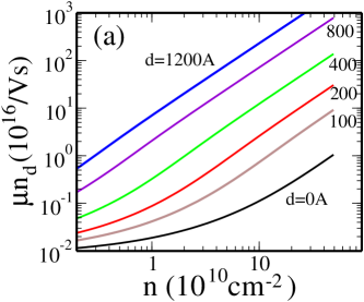
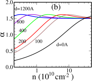
In Fig. 1(a) we show our mobility results for remote dopant scattering as a function of the electron density for various values of the modulation doping separation distance Å (note that implies that the charged impurities are at the GaAsAs-GaAs interface). Since , we show in Fig. 1 the product as a function of for various values of . Our results at the lowest and the highest carrier densities are not reliable due to our neglect of localization and intersubband scattering effects, respectively, but the results should be valid in the cm-2 range without any problem for high-quality samples.

Assuming a high value of cm-2, we see that the maximum intrinsic mobility at cm-2 increases from cm2/Vs for Å to the very large number of cm2/Vs for Å. Since the maximum achieved low-temperature 2D mobility so far has been around cm2/Vs for Å, we conclude that the remote dopants are not the primary mobility limiting mechanism although they may be contributing about 30% of the resistive scattering. In Fig. 1(b) we show that approximate density exponent () of mobility, which has often been discussed in the literature, by writing , i.e. . We note that except for , for remote impurity scattering, and for larger values of . This is simply a reflection of the fact that the remote scatterers are rather ineffectively screened by the 2D carriers, leading to which corresponds to the unscreened limit. We conclude from Fig. 1 that, if all other scattering mechanisms can be eliminated (most importantly, the unintentional background impurities), then at low temperatures, the 2D mobility could easily exceed cm2/Vs at cm-2 provided Å. Note that for large , where with being the 2D Fermi wave vector, , and therefore, as a matter of principle, remote dopant scattering can be reduced indefinitely simply by increasing although in practice this is difficult since inducing carriers in the 2DEG becomes difficult for large .
In Fig. 2, we show our calculated mobility due to scattering by unintentional background charged impurities using the same quantum well parameters, but now with a three-dimensional uniform random background distribution of charged impurities of concentration per unit volume which reside everywhere (both in GaAs and in AlGaAs). Again, , and therefore we show in Fig. 2 our calculated as a function of the carrier density at . For very clean and pure materials as typically used in the very best MBE growth laboratories, is extremely small, and cannot be directly measured by any spectroscopic tools (e.g. DLTS). Assuming cm-3, which is a low estimate, we get cm2/Vs at cm-2. It therefore appears that the current limit to the achievable 2D mobilities in GaAs systems is set entirely by the background unintentional charged impurities, and reducing their level to cm-3 or below should raise the 2D mobility to cm2/Vs or above at low temperatures. To further reinforce the relevance of background scattering, we show as an inset to Fig. 2 the exponent (i.e. ) for background scattering by calculating . The value of agrees well with the corresponding experimentally measured exponent. Note that the exponent decreases as the width of quantum well decreases and the measured exponent in the ultrahigh mobility system is considerably below implied by remote impurity scattering [Fig. 1(a)].
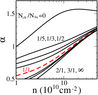
Since the current low temperature () 2D mobility limit in high-quality GaAs structures is set by the Coulomb scattering by charged impurities, mostly by the unintentional background impurities and partially by the remote dopants in the modulation layer, we show in Figs. 3 and 4 some more details on the theoretical mobility arising from the screened Coulomb scattering. Noting that the quantitative details of the background unintentional doping are simply unknown (since their concentration is far too low to be studied spectroscopically), we show in Fig. 3, the calculated mobility exponent (i.e. ) for different combinations of the barrier (i.e. AlGaAs) and the channel (i.e. GaAs) background impurity scattering leaving out the remote dopant scattering. The dashed curve with in Fig. 3 indicates the results shown in Fig. 2 where the 3D random charged impurities are distributed uniformly throughout the background (i.e. both in the GaAs channel and in the AlGaAs barrier). As expected, the exponent decreases as the relative background scattering from the GaAs layer increases with respect to that from the AlGaAs barrier region. This is a direct effect of screening by the 2D carriers themselves which is, of course, stronger (weaker) for the channel (barrier) impurities. For cm-2, the exponent is in excellent agreement with experimental results in the highest mobility variable density gated structures lilly where the 2D mobility has been measured as a function of carrier density. It is noteworthy that in Fig. 3, increases with increasing carrier density, reflecting the well-known dassarma1 ; RMP peculiarity of 2D screening that it becomes weaker (stronger) with increasing (decreasing) carrier density since the relevant dimensionless screening parameter , where () are 2D Thomas-Fermi screening wave vector (Fermi wave vector) goes as by virtue of being density independent in 2D. Thus, for very large density, , we recover the unscreened result . At high density ( cm-2), it is possible that interface roughness scattering (not included in our theory) could start contributing as the 2D electrons are pushed close to the GaAs-AlGaAs interface by the self-consistent confining potential, leading to since the interface roughness is a short-range scattering potential with very weak density dependence.
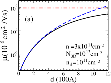
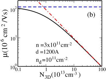
In Fig. 4, we show the combined effects of remote and background Coulomb scattering (i.e. a combination of Figs. 1 and 2) on the 2D mobility at . In Fig. 4(a), we show our calculated mobility as a function of the modulation separation for fixed values of the densities , , and . It is clear that for cm-2 and cm-3, reaches a maximum of around cm2/Vs for Å since the background impurities become dominant for large . Any further enhancement of mobility would necessitate decreasing , which is shown in Fig. 4(b), where we plot as a function of for fixed values of , , and . A 2D mobility of cm2/Vs (the ‘100 millions’ in the title of our paper) can be achieved if can be brought down to cm-2, an extremely small, but not an impossible, number. Results shown in Fig. 4 explicitly demonstrate how depending on the system parameters , , , and , the actual mobility can be enhanced either by increasing or by decreasing , but extremely large 2D mobility would necessarily require large (Å) and small ( cm-3). We show our intrinsic phonon scattering results next, emphasizing that for K, the results of Figs. 1–4 shown above remain unaffected by phonon scattering.
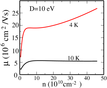
In Fig. 5 we consider the mobility due to acoustic phonon scattering, which is shown as a function of carrier density for K and 10K. For lower temperatures, increases by a large factor ( for deformation potential scattering and for piezoelectric scattering) since one is in the Bloch-Grüniesen range where phonon accupancy is suppressed exponentially stormer_ph . The important point of Fig. 5 is that at K (or even at 4K), the mobility at cm-2 is totally dominated by phonons and becomes cm2/Vs ( cm2/Vs), which is much lower than that for charged impurity scattering. We therefore conclude that it will be impossible to raise 2D mobility above () cm2/Vs at (4)K since acoustic phonon scattering sets the intrinsic limit at these higher temperatures. At 1K or below, however, acoustic phonon scattering is completely suppressed, and the mobility is limited by background charged impurity scattering and, to a lesser degree, by the remote dopant scattering. For example, at the acoustic phonon limited mobility exceeds 100 millions.
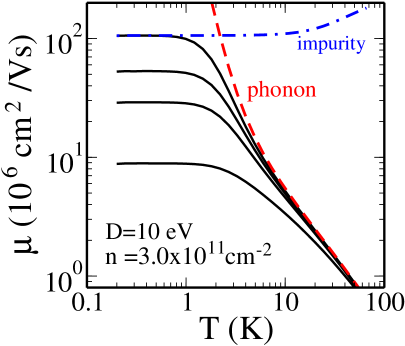
Finally, as a conclusion, we combine the acoustic phonon and background impurity scattering in Fig. 6, by showing how progressive reduction of the unintentional background charge would raise the mobility toward 100 million cm2/Vs provided Å. We estimate that a background impurity density of cm-3 would produce a 2D mobility of cm2/Vs at and cm-2 for Å and cm-2.
This work is supported by Microsoft Q project, DOE Sandia National Lab, and LPS-NSA-CMTC.
References
- (1) H. L. Stormer, R. Dingle, A. C. Gossard, and Wiegmann, Inst. Conf. Ser. London 43, 557 (1978).
- (2) L. Pfeiffer, K. W. West, H. L. Stormer, and K. W. Baldwin, Appl. Phys. Lett. 55, 1888 (1989); J. H. English, A. C. Gossard, H. L. Stormer, and K. W. Baldwin, Appl. Phys. Lett. 50, 1826 (1987).
- (3) M. Heiblum, private communication; L. N. Pfeiffer, private communication.
- (4) C. R. Dean, B. A. Piot, P. Hayden, S. Das Sarma, G. Gervais, L. N. Pfeiffer, and K. W. West, Phys. Rev. Lett. 100, 146803 (2008); J. S. Xia, W. Pan, C. L. Vicente, E. D. Adams, N. S. Sullivan, H. L. Stormer, D. C. Tsui, L. N. Pfeiffer, K. W. Baldwin, and K. W. West, Phys. Rev. Lett. 93, 176809 (2004); J. P. Eisenstein, K. B. Cooper, L. N. Pfeiffer, and K. W. West, Phys. Rev. Lett. 88, 076801 (2002); M. Dolev, M. Heiblum, V. Umansky, A. Stern, and D. Mahalu, Nature 452, 829 (2008); H. C. Choi, W. Kang, S. Das Sarma, L. N. Pfeiffer, and K. W. West, Phys. Rev. B 77, 081301(R) (2008); W. Pan, J. S. Xia, H. L. Stormer, D. C. Tsui, C. Vicente, E. D. Adams, N. S. Sullivan, L. N. Pfeiffer, K. W. Baldwin, and K. W. West, Phys. Rev. B 77, 075307 (2008); I. P. Radu, J. B. Miller, C. M. Marcus, M. A. Kastner, L. N. Pfeiffer, K. W. West, Science, (2008) in press; arXiv :0803.3530.
- (5) S. Das Sarma, M. Freedman, and C. Nayak, Phys. Rev. Lett. 94, 166802 (2005); C. Nayak, S. H. Simon, A. Stern, M. Freedman, S. Das Sarma, Rev. Mod. Phys. (2008) in press; arXiv:0707.1889.
- (6) T. Kawamura and S. Das Sarma, Phys. Rev. B42, 3725 (1990).
- (7) T. Kawamura and S. Das Sarma, Phys. Rev. B45, 3612 (1992).
- (8) S. Das Sarma and E. H. Hwang, Phys. Rev. Lett. 83, 164 (1999); Phys. Rev. B 61, R7838 (2000); 69, 195305 (2004).
- (9) T. Ando, A. B. Fowler, and F. Stern, Rev. Mod. Phys. 54, 437 (1982)
- (10) M. P. Lilly, J. L. Reno, J. A. Simmons, I. B. Spielman, J. P. Eisenstein, L. N. Pfeiffer, K. W. West, E. H. Hwang, and S. Das Sarma, Phys. Rev. Lett. 90, 056806 (2003); S. Das Sarma, M. P. Lilly, E. H. Hwang, L. N. Pfeiffer, K. W. West, and J. L. Reno, Phys. Rev. Lett. 94, 136401 (2005)
- (11) H. L. Stormer, L. N. Pfeiffer, K. W. Baldwin, and K. W. West, Phys. Rev. B 41, 1278 (1990).