Coexistence of anomalous field effect and mesoscopic conductance fluctuations in granular aluminium
Abstract
We perform electrical field effect measurements at 4 K on insulating granular aluminium thin films. When the samples size is reduced below m, reproducible and stable conductance fluctuations are seen as a function of the gate voltage. Our results suggest that these fluctuations reflect the incomplete self-averaging of largely distributed microscopic resistances. We also study the anomalous field effect (conductance dip) already known to exist in large samples and its slow conductance relaxation in the presence of the conductance fluctuations. Within our measurements accuracy, the two phenomena appear to be independent of each other, like two additive contributions to the conductance. We discuss the possible physical meaning of this independence and in particular whether or not this observation is in favor of an electron glass interpretation of slow conductance anomaly relaxations.
pacs:
72.80.Ng, 61.20.Lc, 73.23.-b, 73.23.HkI Introduction
An anomalous field effect in disordered insulators has been first observed in 1984 by Adkins et al. AdkinsJPC84 . In their experiment, an insulating discontinuous gold film was used as the conducting channel of a MOSFET structure. At low temperature, the conductance of the film was found to increase when the gate voltage was swept away from its cooling value, whatever the sweep direction. A few years later, Ovadyahu et al. observed a similar conductance dip in insulating indium-oxide (amorphous InOx and crystalline In2O3-x) thin films BenChorinPRB91 . A large number of experiments have been performed since then in the latter systems VakninPRB02 . The conductance was shown to decrease as a logarithm of time after a temperature quench or a sudden gate voltage change. The samples never reach a true equilibrium state even after one week of measurement. Qualitatively similar effects were reported in ultra thin films of Pb and Bi MartinezPRL97 and we published a thorough study of these phenomena in granular Al films GrenetEPJB03 ; GrenetEPJB07 . It is worth noting that doped semiconductors do not show a dip and that slow and glassy like electronic relaxations have been only rarely reported in there DonMonroePRL87 ; PopovicPRL06 .
A priori all these systems have different microstructures: the disorder is ”granular” for discontinuous and granular metal films whereas it is ”homogeneous” (oxygen vacancies and atomic position distribution) for indium-oxide films. Consequently, two different physical pictures have naturally emerged to explain the anomalous field effect and its long relaxation times.
-
-
In InOx films, it was shown VakninPRL98 that the typical relaxation time and the width of the conductance dip depend systematically on the carrier concentration : the larger , the longer the relaxation time and the wider the dip. Moreover, the relaxation time decreases rather sharply below . These results may explain why the anomalous field effect and its slow relaxation are observed in Anderson insulators with a high carrier concentration, like indium-oxide and granular Al, and not in doped semiconductors which usually have much smaller VakninPRL98 . They also suggest that such phenomena reflect the existence of an electron glass at low temperature (we call this hypothesis the intrinsic one). The electron glass existence was theoretically predicted for disordered insulators in 1982 by different authors DaviesPRL82 ; GrunewaldJPC82 ; PollakSEM82 . The combined effects of disorder and unscreened interactions between localized electrons should give rise to a glassy dynamics and correlated motion of electrons at low temperature. The experimental findings of slow conductance relaxations have motivated several theoretical works on the electron glass problem YuPRL99 ; GarridoPRB99 ; TsigankovPRB03 ; GrempelEL04 ; MullerPRL04 ; LebanonPRB05 .
-
-
In granular systems, a different explanation was proposed. It was shown that the conductance dip and its slow relaxation could be qualitatively accounted for by a slow polarization of the dielectric material around the metallic grains GrenetEPJB07 . This idea was first introduced by Adkins et al. AdkinsJPC84 and developed later by Cavicchi and Silsbee CavicchiPRB88 for the interpretation of capacitive measurements on granular films. We call this hypothesis the extrinsic one since according to it, the non equilibrium effects don’t come from the electrons of the metallic grains themselves. Other observations may be in favor of an extrinsic interpretation. Features qualitatively similar to field-gated conductance measurements were found at very low temperature in the dielectric response of amorphous materials to large DC electric fields SalvinoPRL94 . It was also shown that bias voltage changes can induce at room temperature non exponential relaxations and memory effects in the electronic properties of Al-AlOx-Al planar tunnel junctions, the effects being attributed to the metastability of interface states NesbittPRB07 . Interestingly enough, such tunnel junctions are present in our granular Al thin films GrenetEPJB07 . Last, we would like to mention that an extrinsic type of scenario has been recently suggested for indium-oxide films BurinCondmat07 .
The striking similarity between the different experimental results strongly suggests that the same physical process is involved for all the systems. We have already discussed in Ref. GrenetEPJB07 why we believe that the two hypotheses (extrinsic versus intrinsic) could be applied to both granular and homogeneous systems. Up to now and to our point of view, none of the hypothesis has been undoubtedly settled by the experiments. The logarithmic time dependence of the conductance and the simple aging relaxation laws observed after gate voltage changes can be interpreted as the response of independent degrees of freedom with relaxation times such as has a flat distribution over the time scale of the experiments VakninPRB00 ; GrenetEPJB07 . Such an interpretation is obviously independent of the nature of these degrees of freedom (correlated electrons hops, two level systems charge configurations, etc. KozubCondmat08 ). One important difficulty in order to rule out or to establish one hypothesis comes from the absence of quantitative and indisputable predictions directly comparable to experimental data. Whether the intrinsic (electron glass) hypothesis is the correct one or not is of prime interest since the long response times measured (more than hours and days) may constitute a direct experimental evidence of its existence.
To shed light on the actual origin of these slow relaxation phenomena, we choose to perform field effects measurements on small size granular Al thin films. By small size, we mean small enough to observe reproducible gate voltage induced conductance fluctuations and to study if the conductance dip is modified by these fluctuations. In diffusive metals of mesoscopic size, the conductance was shown to be sensitive to details of disorder and even to the motion of single impurities (see Ref. WashburnRPP92 for a review). Changing the gate voltage or the magnetic field modifies the quantum interference effects between elastic diffusion centers responsible for weak localization corrections. At low temperature, this gives rise to the well known Universal Conductance Fluctuations, which are of the order of the quantum of conductance for samples having sizes equal or smaller than the coherence length. Gate voltage or magnetic field conductance fluctuations pattern could therefore be considered as a finger-print of the sample specific realization of disorder.
A similar finger-print exists also at low temperature for hopping disordered systems. Due to the large (exponential) distribution of electron hops probabilities between pairs of localized states, the conductance of small size samples is dominated by a few critical hops or microscopic resistances ShklovskiiEfros84 . The gate voltage and the magnetic field could change the values and the positions of the dominant resistances, giving rise to conductance fluctuations of quantum ShklovskiiSpivak91 ; FengPRL91 and/or geometrical origin LeePRL84 . The typical distance between the dominant resistances defines the length scale above which the conductance starts to self-average ShklovskiiEfros84 ; FengPRL91 . This length scale could be orders of magnitude larger than the phase coherence length (the hopping length in the variable range hopping regime) when the spread of hops resistances is very large. Indeed, conductance fluctuations have been observed in samples of sub-micrometer FowlerHT91 ; LadieuJPI93 ; HofheinzEPJB06 micrometer AronzonPA97 ; SavchenkoSM91 and millimeter sizes MillikenPRL90 ; PopovicPRB90 . Telegraphic noise of individual fluctuators was also identified SavchenkoSM91 ; CobdenPRL92 ; HofheinzEPJB06 . Depending on the system parameters and the temperature, the amplitude of the fluctuations can be as large as the conductance itself. As we will discuss in more details in Sect. III.2, similar gate voltage conductance fluctuations are expected in our insulating granular Al films. Since the fluctuations pattern obtained by scanning the gate voltage is believed to reflect the spatial and energetic distribution of microscopic resistances, it is especially interesting to see how it is influenced by the field effect anomaly and its slow relaxation. We published preliminary results in Ref. GrenetTrieste03 ; GrenetEPJB07 and similar investigations were reported very recently on In2O3-x films OrylanchikPRB07 .
In Sect. II we will present samples elaboration and measurement techniques. Sect. III is devoted to the study of reproducible conductance fluctuations in samples of micrometer size. The data are shown to be in agreement with a percolation model applied to strongly inhomogeneous media. In Sect. IV, the conductance fluctuations are studied in relation to the anomalous field effect (the conductance dip) and slow relaxation phenomena. The conductance dip formation and its slow response to gate voltage changes are shown to have no influence on the fluctuations pattern. Conversely, the existence of conductance fluctuations does not modify the conductance dip parameters.
II Samples and experimentals
II.1 Samples elaboration
The samples used in this experiment are MOSFET devices in which the conducting channels are made of insulating granular Al thin films. To obtain them, granular Al is evaporated on top of a heavily doped Si wafer (the ”gate”) covered with a 100 nm thick SiO2 insulating layer (the ”gate insulator”). The evaporation was done either through a hand made mask (HM samples) or through a resist mask patterned by classical electronic lithography techniques (EL samples, see Fig. 1). In this last case, 20 nm thick Au contact pads are evaporated prior to resist mask fabrication, whereas for hand made masks, Al contact pads could be evaporated on top of granular Al films without opening the vacuum chamber of the evaporator.
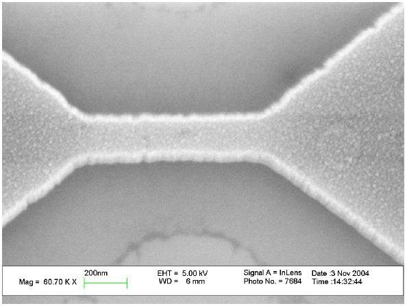
Granular Al films are deposited by e-beam evaporation of Al under a controlled pressure of oxygen. We focus here on samples lying on the insulating side but still close to the metal-insulator transition. The electrical resistance per square at 4 K is tuned between a few M to a few G by slightly increasing the oxygen pressure. Typical parameters are an Al evaporation rate of 2Å/s and an oxygen pressure around mbar. The film thickness is 20 nm for hand made samples and 40 nm for samples made by electronic lithography. The microstructure of the films was already discussed in Ref GrenetEPJB07 . They are believed to consist of Al grains with typical diameters of 5 nm separated by thin insulating AlOx barriers.
II.2 Electrical measurements
The electrical resistance of the granular Al channels was measured in a two contacts configuration. The sample was DC or AC voltage biased and the resulting current was measured through a home made or Femto DLPCA-200 current amplifier. A DC voltage was applied to the gate and could be swept between -30 V and 30 V. No current leak through the gate insulator was detectable in this voltage range. DC voltage sources for the gate and the bias were Yokogawa 7651 or AOIP SN830. AC measurements (frequency between 10 Hz to 200 Hz, depending on the sample resistance) were done with Signal Recovery 7265 or Stanford SR810 Lock In amplifiers.
All the measurements presented below have been done at low bias voltages, in the linear regime of the I-V curves: typical bias voltage is 50 mV for a 50 m long channel.
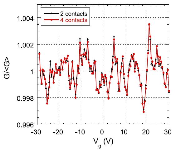
Some samples made by electronic lithography displayed pronounced non linear I-V effects for unexpectedly low voltages compared with hand made samples of similar sizes. They were not used in this study. For hand made samples, the absence of contacts effects in the measured conductance was carefully checked. First, I-V curves were measured for samples of different lengths and it was checked that they depend only on and the electric field across the granular Al channels. Second, for one not too resistive sample (M) long and wide, we compared 2 and 4 contacts measurements. The measured conductances were very close (the difference is of the order of the instruments precision) and the gate voltage fluctuations patterns to be discussed in this paper were practically indistinguishable (see Fig. 2).
III Conductance fluctuations in small samples
III.1 A reproducible conductance fluctuations pattern
When the samples size falls below , clear and well resolved fluctuations of the electrical conductance are visible as a function of the gate voltage at 4 K. The typical relative amplitude is 0.1% for a sample.
The fluctuations pattern does not depend on the measurement conditions. It is independent of the gate voltage sweep parameters (sweep rate between to , sweep direction, etc.), of the instruments used (gate and bias voltage sources, current amplifiers) and of the working frequency (DC or AC measurements). Indeed, in addition to the test of Fig 2, the dependence of the fluctuations amplitude with the square root of the granular Al channel area (see Fig. 8) makes up an indirect confirmation that the pattern actually comes from the channel itself and not from the contacts.
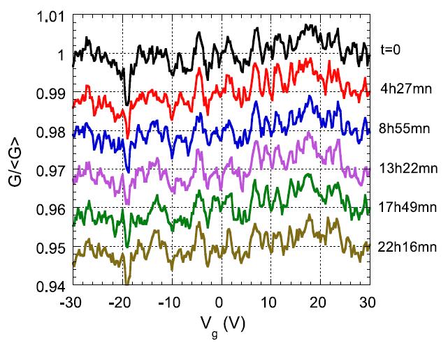
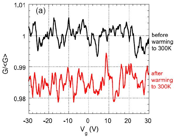
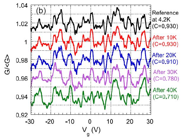
As we can see in Fig. 3, the fluctuations pattern remains stable for one day after a quench at 4.2 K. Some noise is always superimposed on the fluctuations pattern that can be reduced by averaging successive sweeps. A careful check of the long-term stability often reveals a small decrease of the correlation coefficient C between successively measured patterns CorCoeff , reflecting minor changes in the details of the fluctuations. If the sample is warmed up to room temperature and quenched again, the pattern is completely different (see Fig. 4a). A more detailed study indicates that the temperature has to be raised above K in order to change significantly the fluctuations (see Fig. 4b).
The distribution of the conductance values is roughly described by a Gaussian function. In disordered insulators and when the conductance fluctuations are large, asymmetries in the distribution of could give important information about the geometry of the critical resistance network OrlovSSC89a ; HughesPRB96 . For example, a 1D chain will result in a tail towards low conductance values. But even in the sample with a narrow line 100 nm wide, we couldn’t find any systematic asymmetry in the conductance distribution. This is probably due to the fact that our fluctuations are small (1% or less of the conductance value).
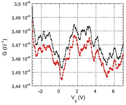
We characterized the fluctuations pattern by its root mean square (rms) amplitude (standard deviation of data). The noise contribution could be subtracted either by working out the average of many scans or by estimating its rms contribution (the variance of the difference between two scans gives an estimate of twice the variance of the noise). In order for to be a well defined number, we used Vg scans with at least one point every 0.5 V and over a range of V. For a given channel, is found to vary by about 10% between different coolings. Fourier Transforms of the fluctuations pattern does not reveal any Vg periodicity and the autocorrelation function falls down to half its value for V. A zoom of the fluctuations on a reduced Vg scale is shown in Fig. 5. We can see that well-reproducible structures of only 0.5 V wide are also present.
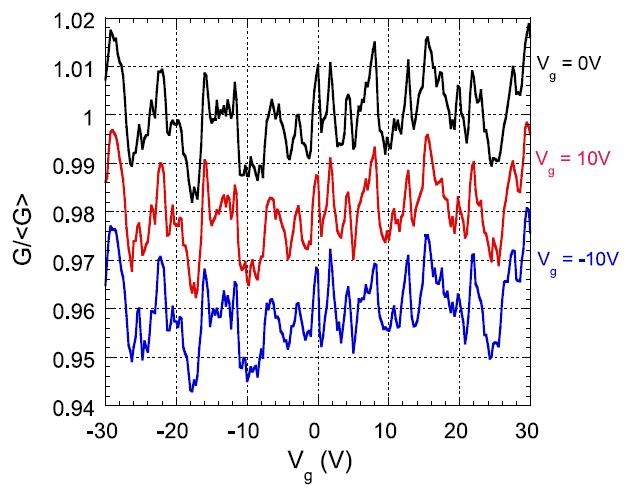
The pattern is also independent of the equilibrium gate voltage which is maintained between the sweeps (see Fig. 6). We will come back in more details to this observation in Sect. IV.
III.2 General picture of the electrical conduction in our granular Al films
We now have to wonder how to understand these conductance fluctuations and the features mentioned above. In particular, how could they be compared to the conductance fluctuations observed in ”homogeneous” disordered insulators, like indium oxide?
As it was mentioned in Sec. II, our insulating granular Al thin films consist of Al grains about 5nm in diameter separated by AlOx tunneling barriers. One important energy scale is the charging energy of an individual grain. Assuming a tunneling barrier thickness of 1 nm and a dielectric constant close to that of Al2O3, we get a charging energy of about 150 K. It is much larger than the thermal energy at 4 K and Coulomb blockade effects are thus important at low temperature in our system. The room temperature R□ of the films spans from 30 to 80 k (HM samples, 20nm thick). It should give a lower bound value for the dominant microscopic tunnel resistances note2 . Even if such values are not much larger than the quantum resistance k, we will neglect quantum fluctuations of charge on the grains in the following discussion.
In a perfectly regular 2D-array of metallic grains (i.e. an array with unique values of inter-grains capacitances C, gate-to-grains capacitances Cg and tunnel resistances between adjacent grains), a global gate voltage Vg induces the same polarization charge in each grain . A naive picture suggests that at low temperature, such a Vg change gives rise to a large and periodic modulation of the array conductance with a period of , similar to what is observed in Single Electron Transistors or SETs. This is clearly not what we are observing here: relative conductance fluctuations are of only few percent or smaller. But as we recall now, this naive picture neglects important sources of potential disorder in the system AdkinsJPC84 ; AdkinsMIT95 .
The first source of disorder is the inevitable presence of grains size and tunnel barriers thickness distributions, which unfortunately we cannot measure easily. They would result in distributions of charging energies, gate-to-grains capacitances Cg and tunnel resistances. But even if a wide distribution of Cg will smooth the Coulomb oscillations for gate voltage larger than , a large gate voltage conductance modulation should still be present at (grains in phase) which is again not observed in our films.
Another important source of random potential comes from the presence of charged impurities or defects trapped in the dielectric environment of the grains (tunneling barrier, substrate and natural oxide layer covering the film). Such trapped charges polarize the metallic grains and induce so called offset charges. The offset charges Q0 are not quantized and could be larger than e. They can be static or dynamic. When a metallic island is connected to bulk electrodes with two tunnel junctions (SET), the current through the device at low bias (in the Coulomb blockade regime) was shown to be very sensitive to tiny changes in the island potential corresponding to offset charges of 10 or below BouchiatThesis97 ; LikharevNMT03 . The existence and the dynamics of offset charges were clearly identified in metal-based transistors made by electronic lithography techniques (typical island size is 1 m) BouchiatThesis97 ; ZimmerliAPL92 ; ZorinPRB96 ; ZimmermanPRB97 ; KrupeninJLTP00 ; HuberReview01 , in scanning tunneling spectroscopy measurements on individual and oxidized metallic grains of nanometer size BentumPRL88 ; WilkinsPRL89 and in planar metal-based tunnel junctions RogersPRL84 ; McCarthyAPL99 . In our experiments, the granular Al films are deposited on a thermally grown SiO2 layer 100 nm thick. We think that, in agreement with results on Al oxidation TanPRB05 , our AlOx dielectric layer around the metallic grains is not stoichiometric with Al2O3 and contains a large concentration of oxygen vacancies. This layer certainly constitutes the main source of potential disorder in our system. The role of interface states in the electronic properties of Al-AlOxAl tunnel junctions was also emphasized in Ref. NesbittPRB07 . Capacitive studies on standard Si-SiO2 wafers covered with an electron-gun evaporated Al layer, indicate typical charge densities about e.cm-2, i.e. about one charge every 10 nm (mainly interface states) SerretThesis02 .
One last source of disorder for the potential of the grains was considered in Ref. CuevasPRL93 ; VergesPRB97 . When the grains are very small, surface effects (irregular shapes and sizes) contribute to random changes in the grains potential that are much larger than the mean energy level spacing , and that could be even larger than the charging energy . For metallic grains of 5 nm in diameter, Cuevas et al. CuevasPRL93 estimate that this effect could by itself ionize more than half of the grains. In our case, by taking the approximate formula (d is the diameter of the grains) and the density of states of bulk Al, we get that is about 4 K.
All these effects together result in a large distribution of offset charges that could exceed many times the electron charge . Such large offset charges distribution is usually unstable with respect to single electron tunneling between the grains. They are (partially) compensated by quantized electrons hops from other grains and/or from the electrodes. Theoretical studies on regular arrays of tunnel junctions have shown that the offset charges configuration that minimizes the electrostatic energy depends on the ratio JohanssonPRB00 ; KaplanPRB03 . In 1D and when , a charge placed on one island is screened on a distance called the soliton length (in units of the array step-size) AverinLikharev91 . When (short screening length limit), it is usually assumed that the system ends with a random and uniform distribution of offset charges between and CavicchiPRB88 ; MiddletonPRL93 . But in the opposite limit (), numerical simulations on 1D arrays have found that starting from a random offset charge distribution, the interactions between electrons on distant grains induce energy favorable electron tunneling between the grains that smooth the potential JohanssonPRB00 . Similar simulations were also done on 2D-arrays smaller than the soliton length KaplanPRB03 . After electrostatic energy minimization, the density of states of single electron addition energies has a Coulomb gap equivalent to what is observed in homogeneous disordered systems (but with a different energy dependence). Moreover, the linear conductance at very low bias voltages () is thermally activated. The activation energy is about and changes in the offset charges configuration induce activation energy fluctuations about 1/3rd of this value (these quantities are almost independent of the size of the system). In our granular Al thin films, a rough estimate gives F and F (soliton length ). Thus, electronic correlations between the grains may play an important role, even if the soliton length (about 100 nm) is still smaller than the system size. It is worth noting that the understanding of the electronic properties of granular systems is still an active theoretical field BeloborodovRMP07 in spite of decades of research.
For simplicity, we will consider now that we are let with a random potential disorder with a homogeneous distribution of offset charges on the different grains (we neglect electronic correlations). Such a distribution naturally explains why large Coulomb oscillations are not observed as a function of Vg in macroscopic samples AdkinsMIT95 . It also implies (in the regime ) an exponentially large distribution of hopping probabilities between the grains (a distribution in the barrier thicknesses will have the same effect)MullerPRB02 . Therefore, percolation theory results obtained for strongly inhomogeneous media ShklovskiiEfros84 should also describe the conductance of our granular Al films. According to this theory, our Vg fluctuations come from an incomplete self-averaging of the conductance in small size samples (”mesoscopic” fluctuations). Like in homogeneous hopping systems, the conductance is dominated by a small number of critical resistances (which are here single electron transistors, possibly asymmetric) with a typical distance between them given by the correlation length of the critical network (see below). Our stable fluctuations pattern reflects a specific distribution of offset charges on the grains, which we call below the background charge distribution. A gate voltage sweep shifts all the offset charges and changes the conductance and/or the position of the dominant single electron transistors.
Annealing the system to room temperature resets the background charge distribution and completely modify the fluctuations pattern as seen in Fig. 4a (a direct evidence of annealing effects in individual grains was seen in Ref. KuzminJJAP87 ). Our results for annealing at intermediate temperatures (Fig. 4b) may indicate that the background charge distribution is thermally activated. We often observe at 4K a small decrease of the correlation coefficient between Vg scans as time has elapsed, which may correspond to long-term drifts of offset charges at low T.
The absence of periodicity in G(Vg) fluctuations could be simply explained by a distribution in Cg values. Significant conductance modulations occur on a scale as small as V, 10 times smaller than the typical scale e/Cg. It corresponds to an average change in the charge per grain of only 0.1e. If such a strong sensitivity to Vg changes could also come from a large distribution, we believe that the interactions between electrons on distant grains may play an important role. Indeed, numerical simulations on 1D regular arrays have shown that if the soliton length is large, the threshold voltage is sensitive to gate voltage changes that represent a fraction of electrons per grains JohanssonPRB00 . Moreover, the modulation pattern of the conductance is strongly dependent on the actual background charge distribution. Unfortunately, measurements of 2D artificial junction arrays made by electronic lithography are not directly comparable to our work KurdakPRB98 ; LafargeHab01 . They do not study Vg conductance fluctuations in the linear regime but above the threshold voltage (non ohmic regime) and the interactions are usually short-range ( below or close to 1).
III.3 Size and R□ dependence of the conductance fluctuations
In order to measure how the fluctuations amplitude depends on the samples size and resistance, we have produced a large set of HM samples. Sizes are distributed between 15 m and 1 mm, and R□ at 4.2 K between 1 M and 1 G. Unless explicitly mentioned, all the following measurements have been done at 4.2 K. We will show that, in agreement with the previous discussion, most of our results can be interpreted within a general percolation model applied to a system with an exponentially large distribution of microscopic resistances.
III.3.1 Size dependence of the conductance fluctuations
For samples having similar R□, the fluctuations amplitude is strongly dependent on the sample size, the larger the channel area, the smaller the amplitude (see Fig. 7). Indeed, reproducible fluctuations are still measurable on samples of mm size but the rms relative amplitude falls below 0.01%.
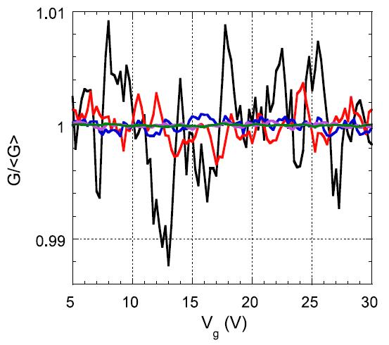
Relative rms amplitudes are gathered on Fig. 8 for three sets of samples with respectively R□ about 5 M , 50 M and 500 M . The relative rms amplitude is found to decrease as the invert of the square root of the channel area. This dependence indicates that the observed fluctuations result from the sum of statistically independent microscopic fluctuations. The length scale L0 at which is given by
| (1) | |||||
| (2) |
where t and S are respectively the thickness and the area of the film. Assuming a 2D regime, we get from the data of Fig. 8 nm for M and 60 nm for M. An interpretation of the length L0 comes from the percolation theory applied to strongly inhomogeneous media ShklovskiiEfros84 . Let’s suppose that we have an exponentially wide range of resistances between the sites i and j of an array, i.e. with an uniform distribution of between . Then, if , the resistance R of the array is that of the critical resistance subnetwork and is given by
| (3) |
The exponential factor is the smallest that first gives percolation when only sites such as are connected. The critical resistance subnetwork includes all the sites such as (sites with larger have a negligible contribution). It is characterized by its correlation radius or homogeneity length L0. In other words, one unavoidable microscopic resistance Rij of the order of the macroscopic one is encountered on a typical length scale L0. L0 is given by
| (4) |
at 3D, at 2D and is the microscopic length of the problem (array step size if the hopping is between nearest neighbors or hopping length in the variable range hopping regime). Changing Vg shifts the Fermi level of the system and therefore the values of the microscopic resistances in the system. This gives rise to conductance fluctuations at the scale L0 and to modifications of the critical resistance network. We will see below whether the condition necessary for the validity of Eq. 3 and Eq. 4 are fulfilled in our samples.
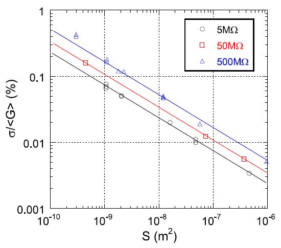
The L0 values extracted from data of Fig. 8 are larger than the film thickness (20 nm for HM samples), confirming a 2D-like regime. Our L0 values are significantly smaller than the homogeneity lengths obtained in In2O3-x thin films (L 300 nm) OrylanchikPRB07 . A study of the fluctuations amplitude dependence on the film thickness (especially around L0) would be very interesting in order to confirm our estimates. The role of the electronic interactions between distant grains on the percolation picture developed above, especially for length scales smaller than the soliton length, should also be clarified.
III.3.2 R□ dependence of the conductance fluctuations
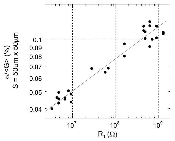
Fig. 8 also emphasizes an increase of the conductance fluctuations amplitude as a function of R□ for a given channel area. The increase is weak: the relative rms amplitude is multiplied by only 2 when R□ rises from 5 M to 500 M (see also Fig. 9).
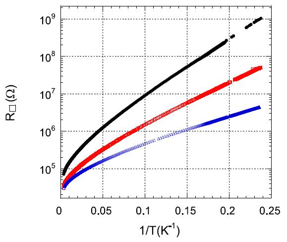
Below K, the resistance temperature dependence is close to an activated law (see Fig. 10)
| (5) |
According to the percolation model described previously,
| (6) |
| (7) |
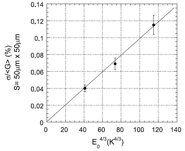
Since for a given channel area the fluctuations amplitude is proportional to L0 (2D-regime) we expect at fixed T:
| (8) |
In Fig. 11, the rms fluctuations amplitudes are plotted as a function of the activation energies E0 extracted from the fits between 4.2 K and 10 K. The data are in good agreement with Eq. 8, taking . The activation energies range between 16 K and 35 K for HM samples with M and G respectively. This justify the use of Eq. 3 and 4 since is much larger than 1: for M and for G (, the critical probability, depends on the array type but is always smaller than 1).
Up to now, the resistance T dependence of our insulating granular Al thin films is still not fully understood in the whole T range and interactions between electrons may play a role. The activated law of Eq. 5 is a reasonable approximation of the low T behavior. Strictly speaking the standard percolation model developed above applies to non-interacting electrons. It is anyway outstanding that the above analysis gives a coherent picture of the data.
III.4 Temperature dependence of the conductance fluctuations
We have also measured the conductance fluctuations as a function of T above 4K for two samples: one HM sample with G ( K) and one EL sample with M ( K). A higher T implies a resistance exponentially smaller. In terms of the percolation theory scenario, the correlation length is smaller, the number of dominant microscopic resistances increases in the system which finally reduces the relative fluctuations amplitude. According to Eq. 7, we expect:
| (9) |
With at 2D, at 3D.
The results for the two samples are presented in Fig. 12 and Fig. 13. The agreement with the percolation theory predictions is only qualitative. The relative amplitude decreases as T is increased (see Fig. 12a). The decrease is well described by the power law Eq. 9 but the exponents are above the expected ones (=2 and 1.7 for respectively the HM and the EL sample, see Fig. 12b) TFluctuations .
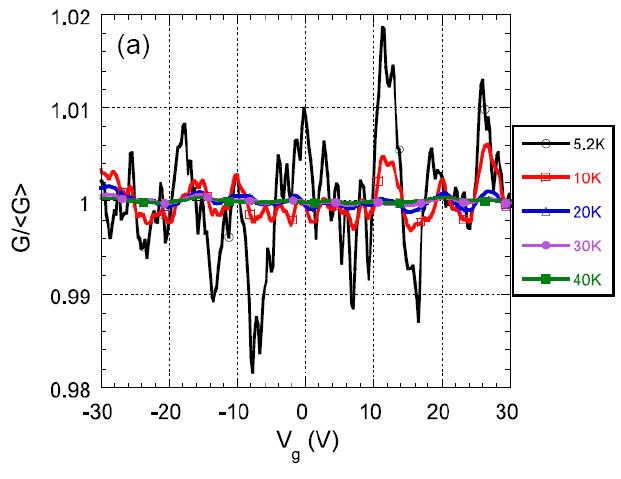
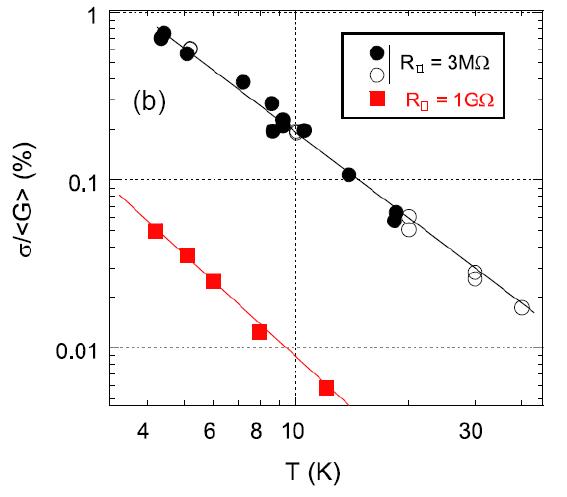
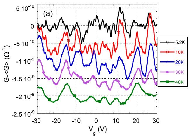
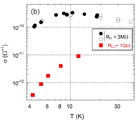
As illustrated on Fig. 13a and b, the absolute rms fluctuations amplitude first increases and then decreases slightly above K. In Fig. 13a, it is seen for the EL sample that the positions of the main structures are unchanged below 20 K (the autocorrelation function width at half value is indeed constant in that T range) and that they are smoothed significantly above. If we still don’t know how to explain the observed T dependencies of Fig. 12 and Fig. 13, the extension of the measurements down to lower T may bring interesting information on this problem.
IV The anomalous field effect in presence of the conductance fluctuations
One main goal of these experiments was to study the anomalous field effect and its slow relaxations in presence of the conductance fluctuations. Slow conductance relaxation phenomena in our macroscopic (with negligible fluctuations) granular Al films have been described in details in Ref. GrenetEPJB03 ; GrenetEPJB07 .
IV.1 Time evolution of the conductance dip
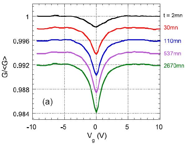
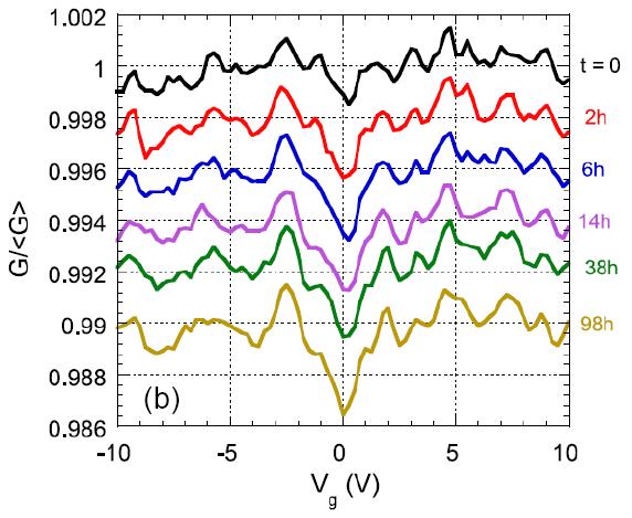
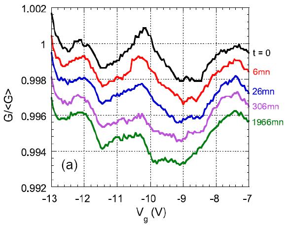
In macroscopic samples maintained under a fixed gate voltage Vgeq at 4.2 K, a fast gate voltage sweep reveals a conductance dip in the G(Vg) curves, symmetric and centered on Vgeq. The dip amplitude was found to increase as a logarithm of the time elapsed since . The formation of a conductance dip after a quench at 4.2K under V is illustrated in Fig. 14a. The same protocol has been followed in Fig. 14b but on a smaller sample ( channel). The conductance dip is still present but superimposed on the conductance fluctuations pattern described previously. The two effects are here of equal magnitudes. The striking feature is that the fluctuations pattern is not affected by the digging of the conductance dip, neither for Vg values within the conductance dip range ( V around Vgeq) nor out of this range. Actually, long-term changes are also visible in the fluctuations of Fig. 14b, but they are weak and similar to what is sometimes seen after a quench in samples where the conductance dip is not visible. Since the fluctuations and the noise amplitude increases when the sample area is reduced (which is not the case for the dip amplitude, see Sect. IV.2), the conductance dip is not visible in too small samples (channels size below . This was for example the case for the EL sample pattern of Fig. 6.
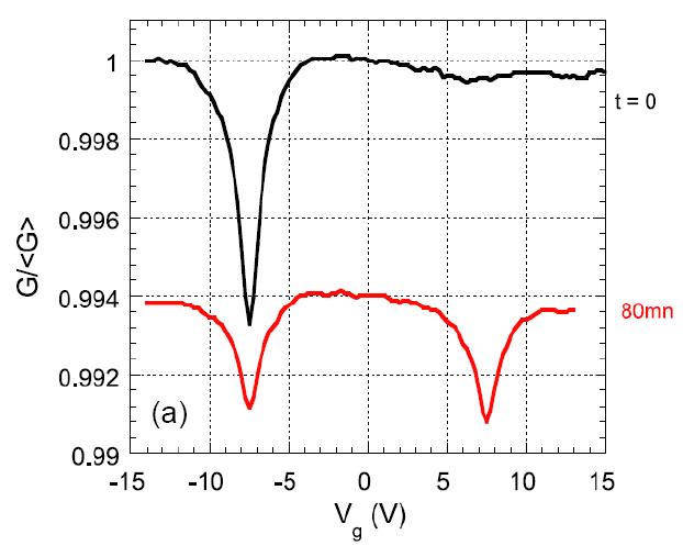
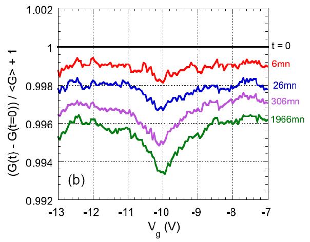
We have also tested a second procedure. Once the sample has been kept for a long time (days) under Vgeq1, the gate voltage is changed to a different value Vgeq2. The results are illustrated for a macroscopic sample in Fig. 15a: a new dip is formed at Vgeq2 while the old dip at Vgeq1 is slowly erased. In microscopic samples (see Fig. 15b), the conductance dip behaves similarly and the fluctuations pattern is essentially unchanged under the displacement of the conductance dip.
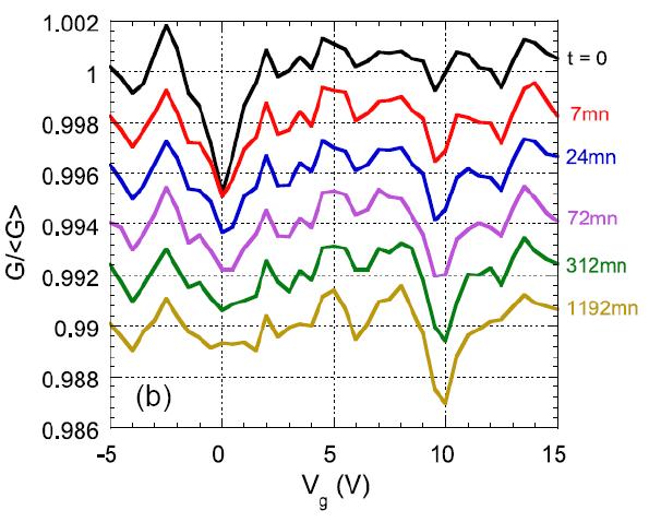
This is even clearer in Fig. 16a and b, where similar data are presented for a microscopic sample but on a reduced Vg range around Vgeq2. By subtracting the curve at (measured under Vgeq1) from the other curves (measured under Vgeq2), the stable fluctuations pattern is eliminated and we are let with a smooth and symmetrical conductance dip (see Fig. 16b). Thus, like for the previous procedure, the fluctuations pattern is not significantly modified by the formation or the erasing of a conductance dip, for gate voltages inside or outside the conductance dip range. We have carefully checked this point in many samples having different R□ values and down to an area of .
IV.2 Parameters of the conductance dip: width and amplitude
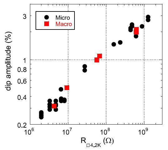
We have compiled conductance dip amplitude data measured on samples of different sizes (lowest area ) and different R□ values. Since the dip is an off-equilibrium property, it is crucial to use exactly the same procedure for all the measurements. In Fig. 17, the parameters are the following: the samples are first maintained under a fixed Vgeq1 for at least 24 h. The gate voltage is then changed to Vgeq2 for 1 hour, creating a new dip, and a gate voltage scan 20 V wide starting from Vgeq2 is recorded (81 points, 4 s/point). The difference between the conductance out of the dip range and the conductance at Vgeq2 gives the new dip amplitude. For microscopic samples (where significant fluctuations are present), a reference scan taken before the change to Vgeq2 is subtracted. The results are independent of the Vgeq1 and Vgeq2 values. Fig. 17 clearly demonstrates that, in spite of a larger data dispersion in microscopic samples (due essentially to a larger noise level), the conductance dip amplitude depends on R□ and not on the sample area in contrary to the fluctuations amplitude. Moreover, the R□ dependence of the dip amplitude is faster than that of the conductance fluctuations. Indeed, its relative value is multiplied by 10 between 2M and 1G , instead of 3 for the fluctuations amplitude (see Fig. 9).
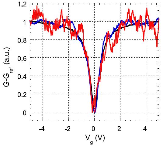
The conductance dip width is also the same in the different samples we have measured, independently of the conductance fluctuations amplitudes and the R□ values (see Fig. 18). As it was already mentioned in Ref. GrenetEPJB07 , the width of the dip in our granular Al films is fixed by the temperature of the measurement and is independent of R□ values and Vg sweep parameters.
IV.3 Time relaxation of the conductance
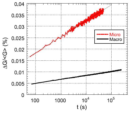
Finally, we have tested if the conductance relaxation laws were modified by the presence of conductance fluctuations. One sample is maintained under a fixed gate voltage during a few days and we follow the conductance response to a sudden change of Vg. In macroscopic samples GrenetEPJB07 , after a fast increase, the conductance decreases as a logarithm of the time elapsed since Vg was changed. In presence of conductance fluctuations, the decrease is noisier but is still described by a logarithm of time (see Fig. 19).
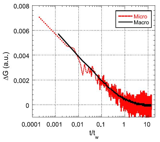
We have also tested the so called two dips experiment VakninPRB02 . In this protocol, the sample is maintained for a long time under Vgeq1, a new dip is formed at Vgeq2 during a time tw and the evolution of curves is followed when the gate voltage is switched back to Vgeq1. At least when is not too large and in macroscopic samples, the erasing of the Vgeq2 dip amplitude was found to be a universal function of (simple aging) VakninPRB02 ; GrenetEPJB07 . Once again, we have observed the same relaxation curves in macroscopic and microscopic samples (see Fig. 20), whatever the conductance fluctuations amplitude.
IV.4 Discussion
Our measurements demonstrate the following important features:
-
-
the glassy conductance dip is not significantly altered by the samples size down to 20 m. This suggests that the conductance dip doesn’t result from an incomplete self-averaging of random microscopic conductance modulations. Its shape and amplitude are indeed independent of the sample size even when the fluctuations amplitude is of the same order of magnitude. The uncertainty in the conductance dip parameters increases when the sample size is reduced, but this increase comes mainly from a higher noise level
-
-
the conductance fluctuations and the dip seem to be independent from each other. Indeed, the fluctuations pattern is not affected by the formation of the conductance dip, and conversely, the conductance dip is formed whatever the conductance fluctuations amplitude. If we assume that the fluctuations pattern reflects the specific potential landscape of the grains, then we conclude that the formation of the conductance dip does not induce large changes in this potential landscape
-
-
the conductance fluctuations and the dip have different dynamics: the former are essentially static once the sample has been quenched at 4 K, while the dip slowly grows. As we have seen, a dynamics of the fluctuations is induced by heating the samples, while no signature of thermal activation can be observed in the glassy dynamics of the dip GrenetEPJB07 .
The independence of the conductance dip and the conductance fluctuations was also demonstrated recently on In2O3-x thin films down to channel sizes of 2 and with a maximum relative amplitude of the minimum about 10% OrylanchikPRB07 . Our results underline once again the strong similarities between granular Al and indium-oxide.
What conclusions may be drawn from these experimental observations about the origin of the glassy dip? In a simplified intrinsic scenario, the stable fluctuations pattern reflects the static distribution of charges in the dielectric material around the grains whereas the slow conductance decrease (dip formation at constant Vg) comes from slow correlated electron hops. This scenario would naturally explain why the two phenomena are independent and have different dynamics, so that our observations are in qualitative agreement with an electron glass interpretation of the conductance dip. But this simplified picture is certainly not exact in our system. As already discussed in Sect. III.2 for a regular array of tunnel junctions, trapped charges in the dielectric materials around the grains result in a random distribution of offset charges between and only when the grains are independent (). However, this distribution does not minimize the global electrostatic energy when due to interactions between the electrons on distant grains. Tunneling of single electrons between the grains permits a large and fast diminution of the electrostatic energy of the system KaplanPRB03 . The random potential is strongly modified by these fast relaxation processes: the potential landscape is smoothed JohanssonPRB00 , strengthening the Coulomb blockade and opening a Coulomb gap in the density of states of single electron addition energies on the grains KaplanPRB03 . Thus the random potential (and the conductance fluctuations) are partly of electronic origin and cannot be considered decoupled from the electronic degrees of freedom. The conductance dip formation is attributed to the slower part of the electronic degrees of freedom, consisting of correlated electrons hops LebanonPRB05 . Correlated electron hops are still decreasing the global electrostatic energy but they are not able to change significantly the local electrostatic order. As long as the conductance dip relative amplitude is small, it seems reasonable to assume that the slow correlated electron hops only induce small shifts in the grains potential (or possibly rare large shifts). For a given Vg, the critical resistance subnetwork is therefore essentially fixed by the trapped charges in the dielectric material around the grains and by the fast single electrons hops between the metallic grains. In other words, we expect that the conductance dip formation affects only slightly the conductance fluctuations pattern. The apparent observed independence of the two phenomena may thus simply come from the fact that the conductance dip amplitude is still small. To this respect, similar measurements on samples having larger conductance dip amplitudes would be of utmost interest.
According to the extrinsic scenario, the conductance dip formation is the result of a slow response of the background charges around the grains. In a continuous model, this is described as a slow linear polarization of the dielectric surrounding the charged grains. It could be shown by a subtle argument that such a polarization shifts the grains potentials in a way that decreases the electron mobility CavicchiPRB88 . The model was initially developed for an electron transport perpendicular to a 2D-array of independent grains: starting from an uniform distribution of offset charges between and , the polarization completely redistributes the offset charges values, the final effect being to reduce the proportion of grains with offset charges close to or (the ”unblocked” grains). Even if a detailed theory for the transport along a 2D-array of interacting grains is still missing, we think that the polarization could similarly reduce the proportion of low resistance hops in our granular films GrenetEPJB07 . Since the dip amplitude is small and since it doesn’t result from the incomplete self-averaging of a random and strongly fluctuating microscopic quantity, it is reasonable to assume that the part of the polarization responsible for the conductance dip induces either small shifts in the grains potentials or larger shifts but for a small number of grains. If such shifts are triggered off by changes in the charge configuration of two level systems nearby, we believe that the second hypothesis is more realistic. According to Sect. III, the conductance fluctuations are instead associated with large changes in the background charge distribution and consequently in the critical resistance subnetwork. We could then naturally understand why the rare events associated with the formation of a small conductance dip could not influence significantly the fluctuations pattern. However it is more difficult to explain the difference in the conductance dip and fluctuations dynamics. A more quantitative approach of the extrinsic scenario (e.g. via numerical simulations) would be very helpful to see whether it can indeed reproduce the coexistence of the dip and the fluctuations.
V Conclusion
In conclusion, we have observed at 4 K reproducible conductance fluctuations as a function of gate voltage in insulating granular Al thin films of micrometer size. Such fluctuations are stable over days of measurement. Their amplitude depends on the size and the resistance per square of the films in agreement with a percolation model applied to an exponentially wide distribution of microscopic resistances. Such wide distribution comes from the combined effects of a charging energy larger than the thermal energy and an important potential disorder of the grains. To the accuracy of our measurements, the conductance fluctuations pattern is not affected by the slow formation of the conductance dip. Conversely and down to sizes of , the conductance dip parameters are unchanged even when the two phenomena have the same amplitudes. This apparent independence may result mainly from the fact that the conductance dip amplitude corresponds to small changes of the macroscopic conductance (no more than few percent in our case). Our results may be more readily interpreted in the intrinsic context (electron glass origin of the conductance dip), but further theoretical analysis would be needed to definitely rule out the extrinsic scenario.
VI Acknowledgements
We acknowledge M. Müller for fruitful discussions. We also thank Sylvain Dumond and the personnel of NANOFAB services for technical support. This research has been partly supported by the French National Research Agency ANR (contract N∘ANR-05-JC05-44044)
References
- (1) C.J. Adkins, J.D. Benjamin, J.M.D. Thomas, J.W. Gardner, A.J. McGeown, J. Phys. C: Solid State Phys. 17, (1984) 4633.
- (2) M. Ben-Chorin, D. Kowal, Z. Ovadyahu, Phys. Rev. B 44, (1991) 3420; M. Ben-Chorin, Z. Ovadyahu, M. Pollak, Phys. Rev. B 48, (1993) 15025;
- (3) A. Vaknin, Z. Ovadyahu, M. Pollak, Phys. Rev. B. 65, (2002) 134208; Z. Ovadyahu Slow relaxations and nonequilibrium dynamics in condensed matter, Les Houches session LXXVII, edited by J.L. Barrat, M. Feigelman, J. Kurchan, J. Dalibard (EDP Sciences-Springer, 2003).
- (4) G. Martinez-Arizala, D.E. Grupp, C. Christiansen, A.M. Mack, N. Marković, Y. Seguchi, A.M. Goldman, Phys. Rev. Lett. 78, (1997) 1130; G. Martinez-Arizala, C. Christiansen, D.E. Grupp, N. Marković, A.M. Mack, A.M. Goldman, Phys. Rev. B. 57, (1998) R670.
- (5) T. Grenet, Eur. Phys. J. B. 32, (2003) 275.
- (6) T. Grenet, J. Delahaye, M. Sabra, F. Gay, Eur. Phys. J. B. 56, (2007) 183.
- (7) Don Monroe, A.C. Gossard, J.H. English, B. Godling, W.H. Haemmerle, M.A. Kastner, Phys. Rev. Lett. 59, (1987) 1148.
- (8) J. Jaroszyński, D. Popović, Phys. Rev. Lett. 96, (2006) 037403.
- (9) A. Vaknin, Z. Ovadyahu, M. Pollak, Phys. Rev. Lett. 81, (1998) 669; Z. Ovadyahu, Phys. Rev. Lett. 99, (2007) 226603.
- (10) J.H. Davies, P.A. Lee, T.M. Rice, Phys. Rev. Lett. 49, (1982) 758.
- (11) M. Grünewald, B. Pohlmann, L. Schweitzer, D. Würtz, J. Phys. C: Solid State Phys. 15, (1982) L1153.
- (12) M. Pollak, M. Ortuño, Sol. Energy Mater. 8, (1982) 81.
- (13) C.C. Yu, Phys. Rev. Lett. 82, (1999) 4074.
- (14) A. Pérez-Garrido, M. Ortuño, A. Díaz-Sánchez, E. Cuevas, Phys. Rev. B 59, (1999) 5328.
- (15) D.N. Tsigankov, E. Pazy, B.D. Laikhtman, A.L. Efros, Phys. Rev. B 68, (2003) 184205.
- (16) D.R. Grempel, Eur. Phys. Lett. 66, (2004) 854; A.B. Kolton, D.R. Grempel, D. Dominguez, Phys. Rev. B 71, (2005) 024206.
- (17) M. Müller, L.B. Ioffe, Phys. Rev. Lett. 93, (2004) 256403;
- (18) E. Lebanon, M. Müller, Phys. Rev. B 72, (2005) 174202.
- (19) R.E. Cavicchi, R.H. Silsbee, Phys. Rev. B. 38, (1988) 6407.
- (20) D.J. Salvino, S. Rogge, B. Tigner, D.D. Osheroff, Phys. Rev. Lett. 73, (1994) 268; D. Natelson, D. Rosenberg, D.D. Osheroff, Phys. Rev. Lett. 80, (1998) 4689.
- (21) J.R. Nesbitt, A.F. Hebard, Phys. Rev. B 75, (2007) 195441.
- (22) A.L. Burin, V.I. Kozub, Y.M. Galperin, V. Vinokur, J. Phys.: Condens. Matter 20, (2008) 244135.
- (23) A. Vaknin, Z. Ovadyahu, M. Pollak, Phys. Rev. B. 61, (2000) 6692.
- (24) Such two level systems can also have an intrinsic electronic nature, see V.I. Kozub, Y.M. Galperin, V. Vinokur, A.L. Burin, cond-mat 0805.3840 (2008).
- (25) S. Washburn, R.A. Webb, Rep. Prog. Phys. 55, (1992) 1311.
- (26) B.I. Shklovskii, A.L. Efros, Electronic Properties of Doped Semiconductors (Springer-Verlag, New York 1984).
- (27) B.I. Shklovskii, B.Z. Spivak, Hopping Transport in Solids, edited by M. Pollak and B.I. Shklovskii (Elsevier 1991) 271.
- (28) S. Feng, J.L. Pichard, Phys. Rev. Lett. 67, (1991) 753.
- (29) P.A. Lee, Phys. Rev. Lett. 53, (1984) 2042.
- (30) A.B. Fowler, J.J. Wainer, R.A. Webb, Hopping Transport in Solids, edited by M. Pollak and B.I. Shklovskii (Elsevier 1991) 223.
- (31) F. Ladieu, D. Mailly, M. Sanquer, J. Phys. I France 3, (1993) 2321.
- (32) M. Hofheinz, X. Jehl, M. Sanquer, G. Molas, M. Vinet, S. Deleonibus, Eur. Phys. J. B 54, (2006) 299.
- (33) B.A. Aronzon, V.V. Rylkov, A.S. Vedeneev, J. Leotin, Physica A 241, (1997) 259.
- (34) A.K. Savchenko, A.O. Orlov, E.I. Laiko, V.V Kuznetsov, Superlattices and Microstructures 9, (1991) 297.
- (35) F.P. Milliken, Z. Ovadyahu, Phys. Rev. Lett 65, (1990) 911.
- (36) D. Popović, A.B. Fowler, S. Washburn, P.J. Stiles, Phys. Rev. B 42, (1990) 1759.
- (37) D.H. Cobden, A. Savchenko, M. Pepper, N.K. Patel, D.A. Ritchie, J.E.F. Frost, G.A.C. Jones, Phys. Rev. Lett. 69, (1992) 502.
- (38) T. Grenet, Proceedings of the 10th Conference on Hopping and Related Phenomena, Trieste 2003, Phys. Stat. Sol. C 1, (2004) 9.
- (39) V. Orlyanchik, Z. Ovadyahu Phys. Rev. B 75, (2007) 174205.
- (40) The linear correlation coefficient between two conductance fluctuations patterns and with i=1,…N was calculated according to the usual formula:
- (41) A.O. Orlov, M.E. Raikh, I.M. Ruzin, A.K. Savchenko, Sol. State Com. 72, (1989) 169.
- (42) R.J.F. Hughes, A.K. Savchenko, J.E.F. Frost, E.H. Linfield, J.T. Nicholls, M. Pepper, E. Kogan, M. Kaveh, Phys. Rev. B 54, (1996) 2091.
- (43) At room temperature, the Coulomb blockade is inefficient and the sample resistance is fixed by the distribution of the microscopic tunnel resistances alone. If this distribution width is small () and asuming that we have 4 grains in the thickness of the film, . For a larger distribution, some tunnel resistances would not contribute to the value (too large or too small ) and dominant values stand between (2D case, very large distribution width) and .
- (44) C.J. Adkins, Metal Insulator Transitions Revisited, edited by P.P. Edwards, C.N.R. Rao (Taylor and Francis 1995) 191.
- (45) V. Bouchiat, PhD Thesis, Université Paris 6 (1997).
- (46) K.K Likharev, Nano et MicroTechnologies 3, (2003) 71.
- (47) G. Zimmerli, T.M. Eiles, R.L. Kautz, J.M. Martinis, Appl. Phys. Lett. 61, (1992) 237.
- (48) A.B. Zorin, F.-J. Ahlers, J. Niemeyer, T. Weimann, H. Wolf, Phys. Rev. B 53, (1996) 13682.
- (49) N.M. Zimmerman, J.L. Cobb, A.F. Clark, Phys. Rev. B 56, (1997) 7675.
- (50) V.A. Krupenin, D.E. Presnov, A.B. Zorin, J. Niemeyer, Journal of Low Temp. Phys. 118, (2000) 287.
- (51) W.H. Huber, S.B. Martin, N.M. Zimmerman, Proceedings of the 1st International Conference on Experimental Implementation of Quantum Computation, Sydney Australia, January 2001, edited by R.G. Clark (Printon Press)176.
- (52) P.J.M. Van Bentum, R.T.M. Smokers, H. van Kempen, Phys. Rev. Lett. 60, (1988) 2543.
- (53) R. Wilkins, E. Ben-Jacob, R.C. Jaklevic, Phys. Rev. Lett. 63, (1989) 801.
- (54) C.T. Rogers, R.A. Buhrman, Phys. Rev. Lett. 53, (1984) 1272; C.T. Rogers, R.A. Buhrman, Phys. Rev. Lett. 55, (1985) 859.
- (55) K.T. McCarthy, S.B. Arnason, A.F. Hebard, Applied Physics Letters 74, (1999) 302.
- (56) E. Tan, P.G. Mather, A.C. Perella, J.C. Read, R.A. Buhrman, Phys. Rev. B 71, (2005) 161401(R).
- (57) E. Serret, PhD Thesis, Université Joseph Fourier Grenoble (2002).
- (58) E. Cuevas, M. Ortuño, J. Ruiz, Phys. Rev. Lett. 71, (1993) 1871;
- (59) J.A. Vergés, E. Cuevas, E. Louis, M. Ortuño, Phys. Rev. B 56, (1997) R7045.
- (60) J. Johansson, D.B. Haviland, Phys. Rev. B 63, (2000) 014201; J. Johansson, PhD Thesis, Royal Institute of Technology Stocholm (2004).
- (61) D.M. Kaplan, V.A. Sverdlov, K.K Likharev, Phys. Rev. B 68, (2003) 045321.
- (62) D.V. Averin, K.K. Likharev, Mesoscopic phenomena in Solids, edited by B.L. Altshuler, P.A. Lee and R.A. Webb (1991)173.
- (63) A.A. Middleton, N.S. Wingreen, Phys. Rev. Lett. 71, (1993) 3198.
- (64) I.S. Beloborodov, A.V. Lopatin, V.M. Vinokur, K.B. Efetov, Rev. Mod. Phys. 79, (2007) 469.
- (65) K.-H. Müller, J. Herrmann, B. Raguse, G. Baxter, T. Reda, Phys. Rev. B 66, (2002) 075417.
- (66) L.S. Kuzmin, K.K. Likharev, Jap. Journal of Applied Physics 26, (1987) 1387.
- (67) C. Kurdak, A.J. Rimberg; T.R. Ho, J. Clarke, Phys. Rev. B 57, (1998) R6842; C. Kurdak, A.J. Rimberg, T.R. Ho, J. Clarke, J.D. Walker, Physica E 5, (2000) 274.
- (68) P. Lafarge, J.J Meindersma, J.E. Mooij, Czechoslovak Journal of Physics 46, (1996) 2361; P. Lafarge, Habilitation à diriger des recherches, Université Joseph Fourier Grenoble (2001).
- (69) There are many problems with the use of the percolation theory and Eq. 9 in our samples. First, the T dependence of the resistance is not really activated above 10K (see Fig. 10). Second, the percolation theory results are only valid if is much larger than 1 ShklovskiiEfros84 , which may be the case in both samples at 4K () but certainly not at 30 K for the EL sample (). Finally, estimates for L0 at 10 K in the HM sample gives about 10 nm (with the use of the 3D Eq. 2), which is quite close to the grains diameter.