Complex microwave conductivity of Pr1.85Ce0.15CuO4-δ thin films using a cavity perturbation method
Abstract
We report a study of the microwave conductivity of electron-doped Pr1.85Ce0.15CuO4-δ superconducting thin films using a cavity perturbation technique. The relative frequency shifts obtained for the samples placed at a maximum electric field location in the cavity are treated using the high conductivity limit presented recently by Peligrad et al. Using two resonance modes, TE102 (16.5 GHz) and TE101 (13 GHz) of the same cavity, only one adjustable parameter is needed to link the frequency shifts of an empty cavity to the ones of a cavity loaded with a perfect conductor. Moreover, by studying different sample configurations, we can relate the substrate effects on the frequency shifts to a scaling factor. These procedures allow us to extract the temperature dependence of the complex penetration depth and the complex microwave conductivity of two films with different quality. Our data confirm that all the physical properties of the superconducting state are consistent with an order parameter with lines of nodes. Moreover, we demonstrate the high sensitivity of these properties on the quality of the films.
pacs:
74.25.Nf, 74.72.-h, 74.78.-w, 74.78.BzI INTRODUCTION
In high- cuprate superconductors the study of the pairing symmetry remains a very active field of research and microwave measurements using resonant structures have shown to be particularly useful to detect its signatures. Indeed, when a microwave resonant cavity is loaded with a conducting sample, we can measure shifts of the resonance frequency and of the quality factor Q, which can be related to the real and imaginary parts of the complex conductivity CASIMIR ; WALDRON ; HALBRITTER . Based on the two-fluid model for a superconductor, condensed pairs and quasiparticles both contribute to which in turn determine the temperature dependence of the magnetic penetration depth and the quasiparticle relaxation rate BONN1993 .
The -wave symmetry is now well established in hole-doped cuprates superconductors HARDY1993 ; JACOBS1995 ; LEE1996 ; KITANO1998 . However, the situation remains controversial in electron-doped ones KOKALES ; PROZOROV ; SNEZHKO . When single crystals are used, residual microwave absorption is generally measured in the superconducting state and this could impede any precise determination of . This residual absorption is likely due to an inhomogeneous oxygen reduction process over the volume of the crystal, a reduction which is mandatory to induce the superconducting state. In this respect, thin films of these materials appear more adapted to microwave experiments. Indeed, high-quality thin films can be grown by pulsed laser ablation on appropriate substrates. Their small thickness and an in-situ post-annealing ensures a homogeneous reduction over the complete volume of the sample. There is, however, an important difference between microwave measurements of thick samples (single crystals) and thin samples (thin films) which has not been completely overcome yet experimentally.
The perturbation of a microwave cavity by a small sample of variable conducting properties is an old problem that has been treated with different approaches for thin superconducting films SCHAUMBURG1992 ; SCHAUMBURG1994 ; PELIGRAD1998 . However, a general procedure proposing to treat the cavity loaded with a perfect conductor sample as the unperturbed state and to find the shifts when the sample becomes a non-perfect conductor, appears particularly promising for high conductivity thin films. A general expression has been obtained for two intracavity arrangements and analytical solutions were found for the slab geometry of a thin film PELIGRAD1998 ; PELIGRAD2001 . The general solution for the complex frequency shift reduces to the Shchegolev formula SHCHEGOLEV in the depolarization limit when the microwave electric field fully penetrates the sample, and to the skin depth regime when the microwave penetration depth becomes smaller than the size of the sample and the complex frequency shift is related to the surface impedance KLEIN . Thin films having different thicknesses and conductivity can thus be treated anywhere between the depolarization regime and the regime close to the skin depth one PELIGRAD2001 . However, the high-temperature superconducting thin films are grown on dielectric substrates having relative permittivity around 20. Hence, when the sample is introduced in the microwave cavity, the substrate changes the field configuration asymmetrically around the sample and modifies the frequency shifts. A method has been proposed to mimic this asymmetric solution by introducing the concept of a fictitious substitute sample. This method has been tested on thin films of hole-doped cuprates mounted in a cylindrical cavity resonating in the TE111 mode PELIGRAD2001 .
In this paper we present microwave measurements on optimally doped Pr1.85Ce0.15CuO4-δ (PCCO) thin films grown on a substrate mounted in the electric field of a rectangular cavity. We use the general solution for the complex frequency shift in microwave electric field in the high conductivity limit PELIGRAD1998 . However, to deduce the complex conductivity from the measured frequency shifts, the fictitious substitute sample method could not be applied to our measurements to take into account the impact of the dielectric substrate. We rather propose a modified version of the method presented by Peligrad et al. exploiting the measurements of the same sample at two different resonance frequencies and by analyzing different substrate configurations. Then, the frequency shifts are transformed into complex penetration depth and microwave conductivity data. These results obtained on two films of different quality are discussed in terms of a two-fluid model. The characteristics of the superconducting state are found to be very similar to the ones obtained in the hole-doped cuprates.
II EXPERIMENT
The PCCO thin films were grown by pulsed laser deposition on standard substrates and their thickness was measured with a scanning electronic microscope at grazing incidence giving a precision of 5 nm. Prior to the microwave measurements, the films were also characterized by four-probe resistivity and AC magnetic susceptibility measurements were performed in a PPMS from Quantum Design between 4 and 300 K. For the two films investigated here, we give in Table 1 the values of the thickness , the critical temperature and the minimum value of the resistivity appearing between 14 and 15 K when a magnetic field of 9T suppresses the superconducting state FOURNIER1998 . is determined from the microwave experiment as indicated in the next section.
The microwave measurements were performed with a cavity perturbation technique in the transmission mode. We used a rectangular copper cavity for which the TE102 (16.5 GHz) and TE101 (13 GHz) resonance modes could be excited. A synthesized sweeper and a scalar network analyzer are used to acquire the resonance curve of each mode after averaging and smoothing. A lorentzian fit of the curve then yields the resonance frequency and the half width at half maximum . This is done for the cavity with and without the sample installed in the maximum electric field position in order to obtain the relative frequency shifts and . A micrometer screw allows for the displacement of the sample in and out of the cavity at low temperatures. With this set-up the noise level is usually better than 1 kHz. The sample (thin film + substrate) has a slab geometry with typical dimensions 2 x 0.2 x 0.5 mm3, 0.5 mm being the thickness of the substrate. The sample and cavity are inserted in a variable temperature insert that permits to scan the temperature between 2 and 300 K with a Cernox sensor and a Lake Shore temperature controller.
| A | 225(5) | 22.5(1) | 101 6 |
| B | 170(5) | 21.5(1) | 310 40 |
III RESULTS AND DISCUSSION
The relative frequency shifts presented in this section will be treated with the formula valid in the high conductivity limit for a slab oriented with its length along the maximum electric field PELIGRAD1998 . Because our frequency shifts are measured relative to an empty cavity when the formula implies shifts relative to a cavity perturbed by a perfect conductor (unperturbed state), we first describe the appropriate correction to transform one into the other. Then, we explain how the substrate effects are included in the treatment. Finally, the temperature dependence of the complex in-plane penetration depth = - i obtained from the frequency shifts and the subsequent complex conductivity data for two PCCO films are presented and discussed.
III.1 The Unperturbed State
Theoretically, when a slab of a perfect conductor is introduced in the electric field of the cavity, the relative shift in resonance frequency depends only on a geometrical factor = , where and are respectively the filling and the depolarization factors. Then, the difference in shifts between the empty cavity and the unperturbed state should be this constant . Since there is no dissipation in a perfect conductor, there is no change induced in the data. An example of these shifts for sample A, corrected for this factor, is presented in Fig. 1. The shift is almost zero in the superconducting state but increases very rapidly when is approached; a monotonous increase is further observed in the normal state. The shift is negative in the superconducting state with a dip appearing just below which is defined as the temperature where the rate of increase is maximum (indicated by an arrow); in the normal state above , the small shift presents a flat temperature dependence for the 13 GHz mode while a monotonous increase is observed at 16.5 GHz. The temperature and frequency dependence of these relative shifts is fully consistent with a superconducting sample in the high conductivity limit PELIGRAD1998 , except for above for the 16.5 GHz mode. The absence of a flat temperature dependence can be explained by a temperature dependent for this particular mode.
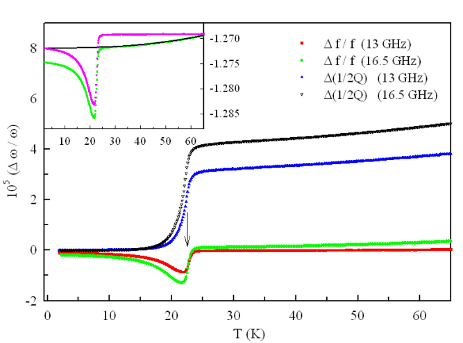
Indeed, a constant factor implies identical temperature dependence of the resonance frequency for an empty cavity and one loaded with a perfect conductor. The TE101 resonance mode at 13 GHz presents only one electric field lobe and the sample which is located at its center perturbs the mode in a symmetrical way; we thus expect a temperature dependence of the resonance frequency very similar to an empty cavity and, thus, a constant . The situation is more complex for the TE102 mode since the sample is located in only one of the two lobes yielding an asymmetrical perturbation of the mode. The resonance frequency as a function of temperature is thus expected to be modified relative to the empty cavity and this yields a which explains the non monotonous temperature behavior observed at 16.5 GHz. We should recall that the temperature dependence of the resonance frequency is due to a progressive increase of the cavity volume above 20 K.
Since the comparison of the complex penetration depth (T) at two frequencies will validate our approach, it is important to correct the data at 16.5 GHz . We show this correction in the inset of Fig. 1. Since the perturbation of the mode is mainly observed above 20 K, we use a polynomial fit to mimic these effects which are subsequently substracted from the original data. If the thin film alone constituted the sample, the constant could be calculated with sufficient precision by associating its geometry to an elongated ellipsoid. However, the substrate makes an undetermined parameter depending on the particular sample and on the resonance mode of the cavity. For each sample, we thus define two parameters and keeping in mind that these parameters are related since the value of the magnetic penetration depth must be frequency independent. We can thus eliminate one degree of freedom by adjusting accordingly the ratio of the two parameters, whose values are chosen to yield the best coincidence of and in the skin depth regime for extracted from the data at 13 and 16.5 GHz ( with the skin depth ). Correction to the shifts at 16.5 GHz is not necessary.
III.2 Dielectric substrate contribution
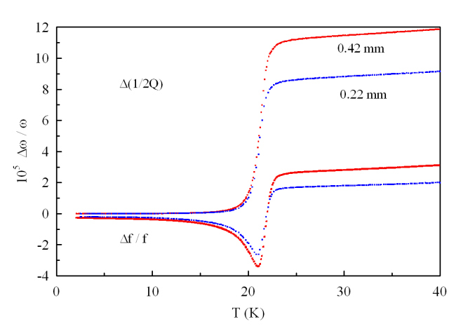
Partly included in the parameter , the substrate modifies also the amplitude of the complex frequency shift relative to the unperturbed state. We propose here a modified procedure adapted to our PCCO films which is based on the comparison of results obtained for different substrate configurations: i) reduced thickness of the substrate; ii) symmetrical sample, substrate-film-substrate. In Fig. 2, we compare the relative frequency shifts at 16.5 GHz obtained for thin film B on a 0.42 mm thick substrate which has been reduced to 0.22 mm after polishing. The increase of thickness does not affect the temperature dependence of the shifts; it acts merely as an amplification factor. Would the situation be similar if the substrate was present on both sides of the film? A second substrate with identical dimensions was mechanically added onto the film. The relative frequency shifts for this configuration -- (SFS) are compared to the - (FS) one in Fig. 3 for the two resonance modes. The temperature dependence of the shifts is again maintained but the amplification factor is increased. As expected, the presence of the substrate increases the frequency shift and decreases the quality factor as can be easily observed above .
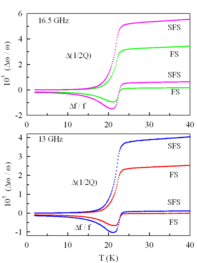
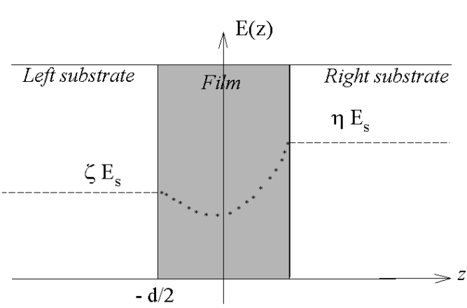
The data of Fig. 2 and Fig. 3 suggest to relate the substrate effects to a scaling factor in the expression connecting the complex frequency shift to the physical properties of the film. This scaling factor is found by considering the electric field configuration of Fig. 4: the substrate on each side of the film acts as an amplifier of the electric field at the interface, a factor on the left and on the right. These factors depend on the thickness and the dielectric constant of the substrate. If we use these new interface conditions to find the electric field profile for the slab geometry and the induced fields and (see appendix), we obtain the following complex frequency shift
| (1) |
where is the complex wave vector. This equation is equivalent to the one obtained for the complex frequency shift from the perfect conductor to an arbitrary state (eq.(18) in PELIGRAD2001 ) except for the scaling factor which is related to the field amplification factors by:
| (2) |
This scaling factor is evaluated by considering the experimental data for the FS configuration (Fig. 2) and the SFS one (Fig. 3) which suggest to write
| (3) | ||||
| (4) |
where we have defined the relative complex frequency shift of the film (F) alone when = 1. If we define as the ratio and we put valid for the data of Fig. 3 (same substrate geometry on both sides of the film), we write the scaling factors as
| (5) |
This last result allows us to express the factor , which represents the deviation from the - configuration, as a function of
| (6) |
Because the undetermined constant , defining , is an adjustable parameter in the final data treatment, we use the shifts of Fig. 3 to determine the factor : practically the same value, 1.59 and 1.62, is respectively obtained at 13 GHz and 16.5 GHz which yields . There is, of course, a dependence of the parameter on the thickness of the substrate as suggested in Fig. 2. The best fit is obtained with a value of reduced by a factor 0.43 when the thickness has been decreased by a factor 0.53. This last result suggests a quasi-linear relationship between and the thickness of the substrate at these frequencies.
III.3 Complex penetration depth : d-wave symmetry
In the preceding sections we have described the tools necessary to extract the complex penetration depth and subsequently the conductivity from our relative frequency shifts data. By adjusting the constant and using the factor determined from Eq.(5) for the FS configuration , we search for each frequency the best superposition of and in the normal state extracted from Eq.(1).
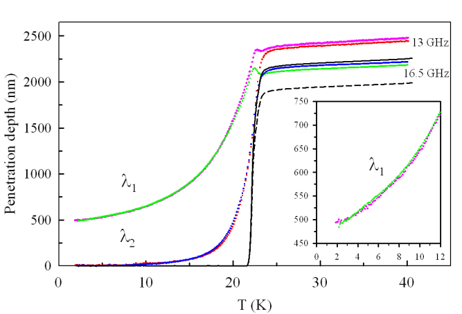
We show in Fig. 5 the complex penetration depth of the thin film A between 2 K and 40 K at 13 GHz and 16.5 GHz. This measurement is analogous to a surface impedance one that could have been performed on a single crystal. However, thin films offer the advantage of obtaining directly the absolute value . In the normal state for , the superposition of and is very good for both frequencies, although better at 13 GHz since no correction of the data is necessary. As expected the penetration depth is larger at 13 than at 16.5 GHz in the normal state, in agreement with the frequency dependence of the skin depth . The monotonous increase of the real and imaginary parts with temperature compares very well with the plots obtained with the DC resistivity measured on the same film and also presented in Fig. 5. The microwave value is just a little larger than the DC one and this is explained by uncertainties on the parameters , and appearing in Eq.(1). In the superconducting state, we observe no frequency effect on on a wide temperature range although we imposed the coincidence at the lowest temperatures only. The extrapolated value towards zero temperature is nanometers; the large uncertainty is attributed to the adjustment of the scaling factor . This value is larger than the one found in the literature LEMBERGER , but is consistent with a higher normal state resistivity. When the temperature is increased from 2 K, increases quasi-linearly first up to 6-7 K ( 17 nm/K) and quadratically after (inset of Fig. 5); then, it goes through a small maximum just below . Such a signature is also observed in other conventional POIRIER and unconventional superconductors ORMENO . When is approached from above, the initial reduction of quasiparticle density leads to a first order reduction in screening from quasiparticles () but only a second order increase in screening from the superfluid fraction. This leads to a peak that moves to lower temperatures on increasing frequency as observed in Fig. 5. In the superconducting state, the imaginary part expresses a rapid reduction of screening by quasiparticles below .
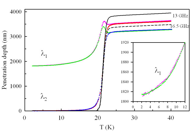
The complex penetration depth of the thin film B between 2 K and 40 K at 13 GHz and 16.5 GHz is presented in Fig. 6. For this sample, the superposition of and in the normal state is excellent at the two frequencies. Here the absolute values are a little smaller than the data calculated from the DC resistivity. In the superconducting state, no frequency effects are observed on a wide temperature range on the real part with an extrapolated value nanometers. When the temperature is increased from 2 K, increases quadratically (inset of Fig. 6, 6 nm/K) and a small peak is still observed just below . The imaginary part appears to decrease more rapidly below for this film compared to the previous one, the reduction of quasiparticle screening being more efficient. This is consistent with the data in Table 1 showing that film A had a higher quality than film B. This is confirmed by a much lower penetration depth and a quasi-linear increasing rate at low temperatures compared to a quadratic one when impurity scattering is more important. Thus, these results appear to be consistent with a -wave order parameter with lines of nodes as already suggested by several other studies.
III.4 Complex conductivity : two-fluid behavior
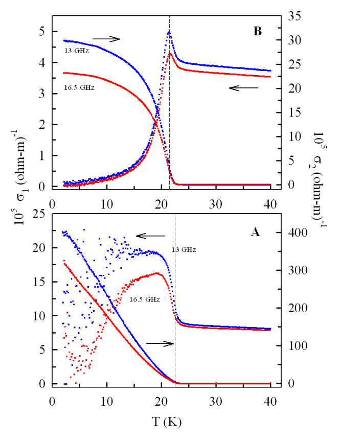
Our microwave penetration depth data are most revealing when transformed into complex conductivity which is presented for both films in Fig. 7. According to the two-fluid model, the real part is related to quasiparticle effects and the imaginary part to the superfluid density. In the normal state, the latter is zero when the former is related to a constant quasiparticle density and a temperature dependent relaxation time . We observe these features in Fig. 7 for both thin films; the temperature dependence of is only due to the relaxation time which increases smoothly with decreasing temperature. The small difference observed between the 13 GHz and 16.5 GHz data do not represent frequency effects; they are due to an imperfect coincidence of and (Fig. 5 and Fig. 6) when adjusting the parameter . In the superconducting state, the behavior of the conductivity is highly sample dependent and we discuss these data separately.
For film A with the best quality, increases first sharply around when the superconducting temperature is approached from above, then presents a wide maximum before decreasing further toward zero at the lowest temperatures. An increase in frequency appears to suppress slightly the maximum. The imaginary part begins to increase weakly above with a faster rate at the superconducting temperature and it goes through a quasi-linear regime below 15 K at both frequencies. This dependence is consistent with a linear increase of the superfluid density at low temperatures, ( being the effective mass). Such a linear behavior was never clearly observed on for optimally doped PCCO thin films LEMBERGER .
Enhanced conductivity effects around are related to superconducting fluctuations which yield generally a peak at on (paraconductivity); however such a peak merges with the wide maximum appearing below which is likely due to a decrease of the relaxation rate of the quasiparticles. These two features appear on different temperature scales in YBCO allowing them to be separated BONN . In our case for the PCCO thin films, their proximity makes them impossible to separate. Moreover, the gradual suppression of the wide maximum with increasing frequency is fully consistent with the relaxation rate scenario discussed above.
The superconducting state conductivity of thin film B is quite different even if the superconducting temperature is lower by only 1 K. presents a small peak confined around and then it decreases rapidly in the superconducting state without showing a frequency dependence. At the same time, increases steeply with only a small smearing around . Below 15 K, both parts of the conductivity vary quadratically with temperature. The small peak on and the weak smearing of at are due to much weaker superconducting fluctuations for this film. The absence of a wide maximum and frequency effects on below , and a similar temperature dependence of the real and imaginary parts below 15 K indicate that only density effects intervene in the quasiparticle contribution. Their relaxation rate which is dominated by impurity scattering does not appear modified substantially in the superconducting state. Impurity scattering also modifies the linear regime of the superfluid density observed in film A to a quadratic one in film B.
These microwave conductivity results appear consistent with a -wave order parameter in these electron-doped cuprates. On the one hand, the highest quality film (A) can be treated in the limit according to the quasi-linear behavior of the penetration depth and of the superfluid density at low temperatures. Concomitantly, quasiparticle effects due to a modified relaxation rate are observed. On the other hand, a film of a lesser quality (B) goes rapidly in the limit yielding a quadratic temperature dependence for and over the same temperature range. Moreover, quasiparticle relaxation rate effects have practically disappeared when superconducting fluctuations, although reduced, still enhance the conductivity at . Compared to film A, the superfluid density appears to be reduced by an order of magnitude in film B although they were grown with the same ablation procedure. Film B, which is substantially thinner than film A, should be more affected by the quality of the interface with the substrate, interface which is likely the source of the increased impurity scattering rate.
IV CONCLUSION
In this paper, we have shown that a microwave cavity perturbation technique can be used to deduce appropriately the absolute value of the penetration depth and its related complex conductivity as a function of temperature for thin films of electron-doped cuprates in their superconducting state. We have treated the thin films, located in the maximum electric field for two resonance modes, using the general solution for the complex frequency shift of Peligrad et al. We have shown how to characterize the unperturbed state, which is essential to the determination of the appropriate frequency shifts, and how to take into account the dielectric substrate effects in the data treatment. Then, with only one adjustable parameter and a pre-determined scaling factor , we have deduced the complex and for two Pr1.85Ce0.15CuO4-δ thin films of slightly different quality. These microwave results reproduce the main characteristics of the superconducting state found in the hole-doped cuprates. We observe a quasi-linear behavior of at low temperatures with a crossover to a quadratic dependence when impurity scattering becomes more important. An important decrease of the quasiparticle scattering rate below must be invoked to interpret the wide conductivity maximum below ; this quasiparticle effect is rapidly quenched by impurity scattering. Finally, important superconducting fluctuations are found around and they could be at the origin of the peculiar temperature dependence of the superfluid density observed in the high quality sample.
Acknowledgements.
The authors thank M. Castonguay and S. Pelletier for their technical support. This work was supported by grants from the Fonds Québécois de la Recherche sur la Nature et les Technologies (FQRNT) and from the Natural Science and Engineering Research Council of Canada (NSERC).APPENDIX: CONTRIBUTION FROM THE SUBSTRATE
To find the spatial dependence of the electric field inside a film having a dielectric substrate on both sides, we start from the following dependence for the slab geometry with the complex wave vector .
| (A.1) |
We then apply the boundary conditions at both interfaces as illustrated in Fig. 4
| (A.2) |
and we obtain the following spatial profiles for the electric and magnetic fields.
| (A.3) |
Then, we calculate the induced fields and inside the slab. Since is different at the two interfaces, we may assume that the field could vary linearly with the distance according to the following relation
| (A.4) |
This will yield a magnetic field varying as
| (A.5) |
with an amplitude determined at the interfaces with the condition
| (A.6) |
With this approximation, we find that the relative permittivity of the sample is not modified by the substrate and we still have the relation.
| (A.7) |
We can now use these expressions for the electric and magnetic fields inside the sample, , , and to calculate the complex frequency shift relative to the perfect conductor state (unperturbed state) with the equation (5) of ref.PELIGRAD2001 to obtain
| (A.8) |
Since the relative permittivity (A.7) is not affected by the substrate within our approximation, we finally obtain the following expression for the relative frequency shift
| (A.9) |
| (A.10) |
where the substrate appears only as a scaling factor . This equation for the frequency shift is identical to Eq.(18) of Ref.PELIGRAD2001 , except for the scaling factor .
When the film thickness is smaller than the penetration depth , we can approximate . The complex penetration depth is finally obtained from the relative frequency shift.
| (A.11) |
References
- (1) H.B.G. Casimir, Philips Res. Rep. 6, 162 (1951).
- (2) R.A. Waldron, Theory of Guided Electromagnetic Waves (Van Nostrand, Reinhold Co., London, 1969).
- (3) J. Halbritter, J. Appl. Phys. 41, 4581 (1970).
- (4) D.A. Bonn, Ruixing Liang, T.M. Riseman, D.J. Baar, D.C. Morgan, Kuan Zhang, P. Dosanjh, T.L. Duty, A. MacFarlane, G.D. Morris, J.H. Brewer and W.N. Hardy, Phys. Rev. B 47, 11314 (1993).
- (5) W.N. Hardy, D.A. Bonn, D.C. Morgan, R. Liang and K. Zhang, Phys. Rev. Lett. 70, 3999 (1993).
- (6) T. Jacobs, S. Sridhar, Q. Li, G.D. Gu and N. Koshizuka, Phys. Rev. Lett. 75, 4516 (1995).
- (7) S.-F. Lee, D.C. Morgan, R.J. Ormeno, D.M. Broun, R.A. Doyle, J.R. Waldram and K. Kadowaki, Phys. Rev. Lett. 77, 735 (1996).
- (8) H. Kitano, T. Hnaguri and A. Maeda, Phys. Rev. B 57, 10496 (1998).
- (9) J.D. Kokales, P. Fournier, L.V. Mercaldo, V.V. Talanov, R.L. Greene and S.N. Anlage, Phys. Rev. Lett. 85, 3696 (2000).
- (10) R. Prozorov, R.W. Gianetta, P. Fournier and R.L. Greene, Phys. Rev. Lett. 85, 3700 (2000).
- (11) A. Snezhko, R. Prozorov, D.D. Lawrie, R.W. Gianetta, J. Gauthier, J. Renaud and P. Fournier, Phys. Rev. Lett. 92, 157005 (2004).
- (12) G. Schaumburg, H.W. Helberg, P. Berberich and H. Kinder, Ann. Physik 1, 584 (1992).
- (13) G. Schaumburg and H.W. Helberg, J. Phys III France 4, 917 (1994).
- (14) D.-N. Peligrad, B. Nebendahl, C. Kessler, M. Mehring, A. Dulcic, M. Pozek and D. Paar, Phys. Rev. B 58, 11652 (1998).
- (15) D.-N. Peligrad, B. Nebendahl, M. Mehring, A. Dulcic, M. Pozek and D. Paar, Phys. Rev. B 64, 224504 (2001).
- (16) L.I. Buravov and I.F. Shchegolev, Instrum. Exp. Tech. 14, 528 (1971).
- (17) O. Klein, S. Donovan, M. Dressel and G. Gruner, Int. J. Infrared Millim. Waves, 14, 2423 (1993).
- (18) P. Fournier, P. Mohanty, E. Maiser, S. Darzens, T. Venkatesan, C.J. Lobb, G. Czjzek, R.A. Webb and R.L. Greene, Phys. Rev. Lett. 81, 4720 (1998).
- (19) M.S. Kim, J.A. Skinta, T.R. Lemberger, A. Tsukada and M. Naito, Phys. Rev. Lett. 91, 087001 (2003); J.A. Skinta and T.R. Lemberger, Phys. Rev. Lett. 88, 207003 (2002).
- (20) A similar peak is observed on the imaginary part of the 16.5 GHz surface impedance of superconducting zinc ( = 0.85 K).
- (21) R. J. Ormeno, A. Sibley and C. E. Gough, Phys. Rev. Lett. 88, 047005 (2002).
- (22) A. Hosseini, R. Harris, S. Kamal, P. Dosanjh, J. Preston, R. Liang, W.N. Hardy and D.A. Bonn, Phys. Rev. B, 1349 (1999).