Modification and Control of Topological Insulator Surface States Using Surface Disorder
Abstract
We numerically demonstrate a practical means of systematically controlling topological transport on the surface of a three dimensional topological insulator, by introducing strong disorder in a layer of depth extending inward from the surface of the topological insulator. The dependence on of the density of states, conductance, scattering time, scattering length, diffusion constant, and mean Fermi velocity are investigated. The proposed control via disorder depth requires that the disorder strength be near the large value which is necessary to drive the TI into the non-topological phase. If is patterned using masks, gates, ion implantation, etc., then integrated circuits may be fabricated. This technique will be useful for experiments and for device engineering.
I Introduction
Recently a new kind of material has been predicted and measured: topological insulators, which do not permit current to flow through their interior but do allow metallic conduction along their surfaces. Kane and Mele (2005); Zhang et al. (2009); Hasan and Kane (2010); Li et al. (2012); Culcer (2012) The conducting states residing on the topological insulator (TI) surface are protected topologically, meaning that they are safeguarded by the bulk’s insulating property from local perturbations as long as a mobility gap is maintained between the bulk bands. In consequence the surface states are only weakly sensitive to fine details of the bulk Hamiltonian, such as lattice structure, details of atomic bonding, or interactions. They are, however, vulnerable to any conduction through the bulk at energies lying in the bulk band gap, and therefore demand a very high-purity bulk. Any engineering of TI devices for either practical or scientific applications will likely use a very pure and unaltered TI bulk, and utilize only the TI’s surface.
There are several compelling motivations for using TI surfaces instead of conventional materials to carry current. Power dissipation may be reduced by the TI’s robustness against disorder. TIs also lock spin to momentum, which will be useful for creating spin-polarized currents and for conducting spin over long distances. They may also host exotic states that could be used for quantum computing, such as Majorana fermions or strongly interacting topological phases. Fu and Kane (2008); Swingle et al. (2011); Maciejko et al. (2010) However these applications all suffer from the topological state’s resilience against the mechanisms usually employed to direct or switch off electronic conduction, such as gating and etching. TI surface states are difficult to control.
In this article we propose a way of engineering TI device properties to match engineering requirements. Our main contribution is the observation that introducing disorder only near the TI’s surface, in a region beginning on the TI surface and extending inward to a depth , is a practical way of controlling the surface states. As the electron moves across the disordered surface of the TI, from time to time it becomes almost trapped at a particular site and dwells there for a while before continuing its journey. This trapping is unable to destroy or localize the in-gap surface state, but it does cause a localized increase in the surface state’s probability density, and our numerical results show a corresponding increase in the in-gap density of states . Moreover, the increased dwell times at individual sites cause, on average, a decrease in the Fermi velocity . The altered density of states and Fermi velocity change also the scattering time , diffusion constant , and coupling constant controlling interactions.
The impact of surface disorder on a topologically protected state is ordinarily limited by the state’s tendency to shift into the clean bulk to avoid disorder. However we can trap the topological state in the disordered region by tuning the disorder strength near the critical value which causes the disordered TI to transit from the topological phase to the non-topological phase.
Our main point is to demonstrate that when the topological state is trapped in the disordered region it is strongly sensitive to the disorder depth . This is a unique control parameter which, if patterned on a TI surface, can create areas with slower conduction and increased density of states, introduce control points that are sensitive to gating voltages, and direct conduction along particular channels.
We emphasize that there are several practical and achievable techniques for producing patterned surface disorder. Already many experiments have studied the effects on TI surfaces of disorder induced by atmosphere, by deliberate introduction of adsorbed molecules and dopants, and even by mechanical surface abrasion. Hsieh et al. (2009); Bianchi et al. (2010); Analytis et al. (2010); Noh et al. (2011); Kong et al. (2011); Tereshchenko et al. (2011); Brahlek et al. (2011); Liu et al. (2012); Valdés Aguilar et al. (2012); Kim et al. (2013) Numerous experiments have also demonstrated that capping can effectively protect a TI surface, so masking and etching techniques are promising, as is ion implantation. Lang et al. (2011)
Ion implantation in particular gives precise control of impurity concentration and depth, and allows control of the Fermi level by mixing ions. This technique has been been developed extensively for applications to semiconductors, but its application to TIs is at an exploratory stage. The related technique of ion milling, useful for controlling sample thickness and for polishing the surface, was first applied to TIs in 2010 and is now in widespread use. Li et al. (2010) Ion implantation was first applied to TIs in studies of the spin response to a magnetic field Vazifeh and Franz (2012); MacFarlane et al. (2014), and more recently has been used to dope the Fermi level Sharma et al. (2014) and to add disorder to the TI surface. Wakeham et al. (2015)
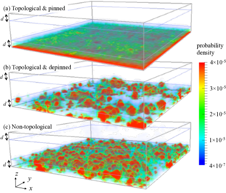
The surface state control which is proposed here is obtained only at the critical disorder , which is generally quite large, roughly the same as the bulk band width , but can be reduced to much smaller values by tuning the Fermi level. Groth et al. (2009); Xu et al. (2012) At small disorder the topological state is pinned at the outer boundary of the disordered region, as seen in Figure 1a. Its conduction is therefore insensitive to the region’s depth. In the opposite case of large disorder the disordered region fills with non- topological states deriving from the bulk band (Figure 1c) Ringel et al. (2012); Schubert et al. (2012); Wu et al. (2013); Wu and Sacksteder (2014) which contribute to conduction, and the conductance and the density of states both depend on . Only near does the topological state depin from the TI’s outer surface and stretch inward to the interface with the clean bulk (Figure 1b), producing conduction which is both topological and sensitive to the disorder depth .
 |
In Section II we analyze these three types of transport and determine in each case how the transport parameters scale with the disorder depth . Next section III presents our numerical model and confirms numerically the existence of the depinned topological state whose transport can be controlled by disorder depth. We conclude with section IV, which discusses how to pattern topological conduction to meet device requirements.
II Scaling Analysis of Disordered Transport
Depending on the disorder strength, three different types of conducting states may be obtained. These states have clear signatures in the dependence of the conductance and the 2-D density of states on disorder depth , which we show in Table 1 and will exhibit in our numerical results. The pinned topological state at is not sensitive to . At the other extreme non-topological states in the disordered region are important. The scattering length of these strongly disordered states is comparable to the lattice spacing and much smaller than the disorder depth, so these states undergo true 3-D diffusive transport, with and both linear in .
In contrast, the depinned topological state at can be identified clearly by the signature of a -linear 2-D DOS , combined with a constant conductance . The linear is caused by the state depinning from the TI surface, while the constant controverts nontopological conduction, which would exhibit 3-D diffusion and a linear conductance.
This signature is unambiguous. The linear DOS cannot be attributed to any non-topological surface or bulk states distinct from the depinned topological state, because all in-gap states are located in the disordered region, which near delocalizes and hosts only extended states like that seen in Figure 1b. In the parallel case of 2-D TIs with edge disorder very few in-gap states are localized, and the conductance remains quantized. Wu et al. (2013); Stanescu et al. (2010); Buchhold et al. (2012) In both 2-D and 3-D at all states mix and participate in the topological conduction.
The depinned state is very remarkable for being simultaneously robustly conducting and extremely disordered. This is seen clearly in Figure 1, where we have calculated the states’ inverse participation ratios (IPR), a measure of their volumes defined by with the -th component of the wave function on the site . These eigenfunctions were obtained by diagonalizing the Hamiltonian using the sparse matrix diagonalization subroutine FEAST built with the Intel Fortran Math Kernel Library. The system size is , and periodic boundary conditions have been imposed in and direction, while the open boundary condition is imposed in direction. The IPR of the wave function of depinned state (Fig. 1(b)) is , an order of magnitude larger than those of the pinned and bulk states (Fig. 1 (a) and (c)), which are and , respectively. In non-topological systems this type of volume reduction would be accompanied by Anderson localization, i.e. the state’s extent along the and axis parallel to the surface would be much smaller than the sample size. Here topology ensures that the depinned state remains conducting and extended across the entire sample.
| Conducting State | |||||||
|---|---|---|---|---|---|---|---|
| topological & pinned | |||||||
| topological & depinned | |||||||
| non-topological |
The depinned state is topologically guaranteed to conduct over large distances, and therefore must have a long-wavelength limit where the average parameters of 2-D surface transport are well-defined, including the 2-D density of states , average Fermi velocity , etc. Wu et al. (2013) We will show that these quantities are strongly dependent on , beginning with the Fermi velocity , the eigenvalue’s derivative with respect to . Its scaling can be determined from the fact that the depinned topological state is not localized. Therefore the eigenvalues within the gap repel each other according to Wigner-Dyson level repulsion, and the energy scale in is set by the level spacing . Wu et al. (2013) The depinned state extends inward to depth , so its 2-D DOS is proportional to , and scales with . Since in strongly disordered samples the momentum scale in is controlled by the inverse of the lattice spacing and is not sensitive to , we obtain .
Next we note that at the scattering length is close to the lattice spacing and independent of . Since , the scattering time grows linearly with , inversely to . We report these scaling relations, along with and the dimensionless coupling constant which controls interaction effects, in Table 1. Castro Neto et al. (2009) Table 1’s results for the depinned state can be determined directly from dimensional analysis by finding each quantity’s scaling with either the scattering time or its inverse, the energy . In summary, and are all very sensitive to the disorder depth , while and are not.
 |
III Numerical Results
We turn to calculations of the effect of disorder depth on and which will confirm numerically the existence of a depinned topological state with the scaling listed in Table 1. The topological surface conduction which interests us is independent of any microscopic details of the Hamiltonian. Therefore we study a computationally efficient minimal tight binding model of a strong TI implemented on a cubic lattice. We leave the TI bulk pure, since the main effects of bulk disorder can be duplicated by narrowing the bulk band gap and increasing the penetration depth in a pure TI.Groth et al. (2009); Guo et al. (2010); Chen et al. (2012); Xu et al. (2012); Kobayashi et al. (2013) We also omit the effects of bulk defects, which are known to dope the Fermi level toward the conduction or valence band depending on the defect type, and at sufficient concentrations also cause a conducting impurity band to be formed inside the bulk band gap. Lee et al. (2014) We will return to doping in section IV. With four orbitals per site, the model’s momentum representation is:
| (1) |
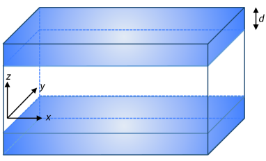
and are gamma matrices in the Dirac representation, is the hopping strength, is the mass parameter, and is the lattice spacing. Liu et al. (2010); Ryu and Nomura (2012); Kobayashi et al. (2013, 2014) This non-interacting model exhibits a bulk band gap in the interval and a single Dirac cone in the bulk gap. To this model we add uncorrelated white noise disorder chosen randomly from the interval , where is the disorder strength. In the 3-D limit this model’s topological phase transition occurs at when the Fermi energy is at the Dirac point. Kobayashi et al. (2013); Sbierski et al. (2014) The disorder is added only on the layers nearest the TI sample’s upper boundary, and also the layers nearest the lower boundary, as shown in Figure 2. Each of these layers has the same disordered strength, and the interior is left clean, so the disorder’s spatial profile is a step function.
We will present numerical results about the global density of states and the conductance . The density of states is defined as , where is the matrix version of the Dirac delta function. We calculate in large slabs, with periodic boundary conditions in the slab plane, using the highly scalable Kernel Polynomial method. Weiße et al. (2006) is approximated with an expansion in its Chebyshev moments, the resulting sum over moments is truncated at some maximum number of moments, and this truncation is smoothed using the Jackson kernel. We verified convergence by systematically recalculating our results with different numbers of moments, going as high as moments. We found that the density of states is self averaging so that samples were sufficient to obtain high accuracy results.
For the conductance we use the Landauer formula , where is the conductance quantum, and average over 100 statistical realizations. is the TI’s transmission matrix, which we compute using the transfer matrix method Pendry et al. (1992); Slevin et al. (2001); Kramer et al. (2005). We calculate the conductance at zero temperature so only states at the Fermi level contribute, in contrast to finite temperatures where the Fermi level is smeared across a range of order . Since the critical disorder strength depends on the Fermi level, at non-zero temperature the conductance will have contributions not only from the topological depinned state, but also from the topological pinned state and the non-topological state. The size of these contributions, and also of the conductance from thermally activated bulk carriers, can be controlled by reducing the temperature.
We minimize leads effects by using metallic leads. Each TI site adjacent to the leads is connected to a perfectly conducting 1-D wire, similarly to network models. We use a slab of height , length between the two leads, and width with periodic boundary conditions along this transverse axis. The scattering length is less than for all disorder strengths greater than , so finite size effects from the sample width and length are small. Wu and Sacksteder (2014) Moreover, because we study disordered boundaries whose maximum depth is layers, the two disordered boundary layers are always separated by at least ten layers of pure non-disordered bulk. Changing the clean bulk’s depth from to while keeping fixed confirms that the conductance is unchanged when the disorder in the boundary is not too large ( at ), but at larger disorder the conductance increases. Since the clean bulk’s depth is equal to , and our numerical results keep fixed, our results on the conductance’s depth dependence underestimate the behavior of a thick slab. This does not affect our qualitative conclusions.
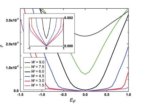
In Figure 3 we focus our attention on the normalized density of states in the bulk gap , where the topological surface states are found. The smallest-disorder curves are linear in , i.e. , which is a hallmark of 2-D Dirac fermions. As seen in the inset, the slope grows with increasing disorder, because disorder causes a decrease in the Fermi velocity . At larger disorder the DOS departs from the linear Dirac form in two intervals near , and by these intervals expand to fill the whole band gap. In these intervals the topological state consecutively becomes strongly disordered, depins, and then is joined by non-topological states in the disordered region. Schubert et al. (2012); Wu et al. (2013) In particular, depinned states occur at two critical energies which in the disorder-free case lie at the band edges but move inward toward the Dirac point as the disorder grows stronger. At the critical energies meet at the Dirac point , and at larger the disordered region no longer hosts topological states. The detailed values of are material dependent, but the qualitative behavior described here is generic to every topological insulator.
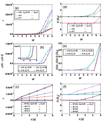
Figure 4 shows signatures of the three types of conducting states in the dependence on depth of the DOS (left panels) and the conductance (right panels). Panels (a) and (d) show that at small disorder both and are independent of , as expected from the pinned topological state. At stronger disorder both quantities become sensitive to , as expected of non-topological states in the strongly disordered region. Panels (c) and (f) demonstrate that the dependence is always roughly linear.
Panels (b) and (e) allow us to pinpoint the transition from no dependence to linear dependence, by plotting the magnitude of the change when is changed from to , and from to . Panel (b) shows that at the DOS becomes dependent on starting at , and the dependence becomes large around . This transition signals depinning from the TI surface, shown in Figure 1b. Panel (e) shows that remains constant in at for , and nearly constant also at . In this region we have constant and linear , which is the signature of the depinned topological state.
In summary, we have confirmed numerically that the depinned state’s conduction obeys the depth dependence in Table 1, which is based on the fact that this state is both very strongly disordered and robustly conducting. In consequence its scattering time scales linearly with the disorder depth and its scattering length is independent of . This determines the depth dependence of all other conduction parameters.
IV Applications
Using this effect, a topological state’s conduction can be engineered and patterned to meet device requirements by introducing a layer of strong surface disorder, and patterning the layer’s depth . must substantially exceed the bulk penetration depth , which is typically in the family of TIs. Zhang et al. (2010) It is necessary that the disorder’s spatial distribution has a step function profile; the disorder strength should be constant from the surface up to depth , and then drop to zero. Ion implantation produces a gaussian depth distribution around a mean depth controlled by the beam energy; a step function distribution may be approximated by applying the beam twice at two different beam energies.
Increasing the density of states of the in-gap surface states will make them less sensitive to bulk defects, which are known to cause bulk conduction by introducing carriers. Depending on the defect type, the defects shift the Fermi level toward either the valence or conduction band. Scanlon et al. (2012); Cava et al. (2013) When disorder is used to increase the surface density of states the Fermi level will be less sensitive to bulk defects and shift further into the gap, increasing the TI quality. In patterned devices points with increased disorder depth and density of states will respond more strongly to external static or ac voltages. Interaction with light also will be increased if the light’s penetration depth exceeds . McIver et al. (2012) Moreover the state’s self-interaction will be increased, which favors transitions to strongly interacting topological phases. Swingle et al. (2011); Maciejko et al. (2010)
Engineered lines of increased on a TI surface can be used to direct the topological current’s flow across the surface, and to divide current flow and later reunite it, similarly to integrated circuits in conventional semiconductor devices. These channels can be controlled by using external gates to locally shift the Fermi level. Because the critical disorder is sensitive to the Fermi level , if the Fermi level is either too large or too small then the topological state will reroute to the boundary of the disordered region and will lose its depth dependence. Therefore external gates can control the density of states at specific points on the TI surface, regulating the current flow through channels, or switching current from one channel to another. In summary, the topological current can be focused, directed along particular channels, and switched, supplying all of the components necessary for realizing topological integrated circuits.
We conclude by discussing a specific device, a spectral analyzer of incoming transient pulses. Its crucial component is a region where the disorder depth grows continuously. A topological state diffusing through this region will experience a spatially non-uniform scattering time . Its diffusion is similar to Brownian motion of classical particles in the presence of a temperature gradient, since the time between Brownian steps varies inversely with temperature. As is well known from the celebrated Ludwig-Soret thermodiffusion effect, the diffusing state will experience an effective force deflecting it along the gradient of and . Platten (2006); Kim (2013); Rahman and Saghir (2014) The deflection is greatest when the topological state’s energy is at the critical value associated with depinning, so the spectral analyzer will spatially resolve incoming pulses according to their component energies.
Acknowledgements.
We thank Quansheng Wu, Liang Du, Alex Petrovic, and Ken-Ichiro Imura for very useful discussion and collaboration, and Ivan Shelykh for his support. This work has been supported by Grants-in-Aid for Scientific Research (B) (Grant No. 15H03700) and Grants-in-Aid No. 24000013. Part of the numerical calculation has been performed on Supercomputer system B of ISSP, Univ. Tokyo.References
- Kane and Mele (2005) C. L. Kane and E. J. Mele, “Quantum spin hall effect in graphene,” Phys. Rev. Lett. 95, 226801 (2005).
- Zhang et al. (2009) Haijun Zhang, Chao-Xing Liu, Xiao-Liang Qi, Xi Dai, Zhong Fang, and Shou-Cheng Zhang, “Topological insulators in bi2se3, bi2te3 and sb2te3 with a single dirac cone on the surface,” Nature Physics 5, 438–442 (2009).
- Hasan and Kane (2010) M. Z. Hasan and C. L. Kane, “Colloquium : Topological insulators,” Rev. Mod. Phys. 82, 3045–3067 (2010).
- Li et al. (2012) Yong-qing Li, Ke-hui Wu, Jun-ren Shi, and Xin-cheng Xie, “Electron transport properties of three-dimensional topological insulators,” Frontiers of Physics 7, 165–174 (2012).
- Culcer (2012) Dimitrie Culcer, “Transport in three-dimensional topological insulators: Theory and experiment,” Physica E: Low-dimensional Systems and Nanostructures 44, 860–884 (2012).
- Fu and Kane (2008) Liang Fu and C. L. Kane, “Superconducting proximity effect and majorana fermions at the surface of a topological insulator,” Phys. Rev. Lett. 100, 096407 (2008).
- Swingle et al. (2011) B. Swingle, M. Barkeshli, J. McGreevy, and T. Senthil, “Correlated topological insulators and the fractional magnetoelectric effect,” Phys. Rev. B 83, 195139 (2011).
- Maciejko et al. (2010) Joseph Maciejko, Xiao-Liang Qi, Andreas Karch, and Shou-Cheng Zhang, “Fractional topological insulators in three dimensions,” Phys. Rev. Lett. 105, 246809 (2010).
- Hsieh et al. (2009) David Hsieh, Y. Xia, Dong Qian, L. Wray, J.H. Dil, F. Meier, J. Osterwalder, L. Patthey, J.G. Checkelsky, N.P. Ong, et al., “A tunable topological insulator in the spin helical dirac transport regime,” Nature 460, 1101–1105 (2009).
- Bianchi et al. (2010) Marco Bianchi, Dandan Guan, Shining Bao, Jianli Mi, Bo Brummerstedt Iversen, Philip D.C. King, and Philip Hofmann, “Coexistence of the topological state and a two-dimensional electron gas on the surface of bi2se3,” Nature Communications 1, 128 (2010).
- Analytis et al. (2010) James G. Analytis, Jiun-Haw Chu, Yulin Chen, Felipe Corredor, Ross D. McDonald, Z. X. Shen, and Ian R. Fisher, “Bulk fermi surface coexistence with dirac surface state in : A comparison of photoemission and shubnikov˘de haas measurements,” Phys. Rev. B 81, 205407 (2010).
- Noh et al. (2011) Han-Jin Noh, Jinwon Jeong, En-Jin Cho, Han-Koo Lee, and Hyeong-Do Kim, “Persistence of surface states despite impurities in the surface of topological insulators,” EPL (Europhysics Letters) 96, 47002 (2011).
- Kong et al. (2011) Desheng Kong, Judy J. Cha, Keji Lai, Hailin Peng, James G. Analytis, Stefan Meister, Yulin Chen, Hai-Jun Zhang, Ian R. Fisher, Zhi-Xun Shen, et al., “Rapid surface oxidation as a source of surface degradation factor for bi2se3,” ACS Nano 5, 4698–4703 (2011).
- Tereshchenko et al. (2011) Oleg Evgen’evich Tereshchenko, K.A. Kokh, V.V. Atuchin, K.N. Romanyuk, S.V. Makarenko, V.A. Golyashov, A.S. Kozhukhov, I.P. Prosvirin, and Aleksandr Andreevich Shklyaev, “Stability of the (0001) surface of the bi2se3 topological insulator,” JETP Letters 94, 465–468 (2011).
- Brahlek et al. (2011) Matthew Brahlek, Yong Seung Kim, Namrata Bansal, Eliav Edrey, and Seongshik Oh, “Surface versus bulk state in topological insulator bi2se3 under environmental disorder,” Applied Physics Letters 99, 012109 (2011).
- Liu et al. (2012) Z.K. Liu, Y.L. Chen, J.G. Analytis, S.K. Mo, D.H. Lu, R.G. Moore, I.R. Fisher, Z. Hussain, and Z.X. Shen, “Robust topological surface state against direct surface contamination,” Physica E: Low-dimensional Systems and Nanostructures 44, 891–894 (2012).
- Valdés Aguilar et al. (2012) R. Valdés Aguilar, A. V. Stier, W. Liu, L. S. Bilbro, D. K. George, N. Bansal, L. Wu, J. Cerne, A. G. Markelz, S. Oh, and N. P. Armitage, “Terahertz response and colossal kerr rotation from the surface states of the topological insulator ,” Phys. Rev. Lett. 108, 087403 (2012).
- Kim et al. (2013) D.J. Kim, S. Thomas, T. Grant, J. Botimer, Z. Fisk, and Jing Xia, “Surface hall effect and nonlocal transport in smb6: Evidence for surface conduction,” Scientific Reports 3 (2013).
- Lang et al. (2011) Murong Lang, Liang He, Faxian Xiu, Xinxin Yu, Jianshi Tang, Yong Wang, Xufeng Kou, Wanjun Jiang, Alexei V. Fedorov, and Kang L. Wang, “Revelation of topological surface states in bi2se3 thin films by in situ al passivation,” ACS Nano 6, 295–302 (2011).
- Li et al. (2010) H.D. Li, Z.Y. Wang, X. Kan, X. Guo, H.T. He, Z. Wang, J.N. Wang, T.L. Wong, N. Wang, and M.H. Xie, “The van der waals epitaxy of bi2se3 on the vicinal si (111) surface: an approach for preparing high-quality thin films of a topological insulator,” New Journal of Physics 12, 103038 (2010).
- Vazifeh and Franz (2012) M. M. Vazifeh and M. Franz, “Spin response of electrons on the surface of a topological insulator,” Phys. Rev. B 86, 045451 (2012).
- MacFarlane et al. (2014) W. A. MacFarlane, C. B. L. Tschense, T. Buck, K. H. Chow, D. L. Cortie, A. N. Hariwal, R. F. Kiefl, D. Koumoulis, C. D. P. Levy, I. McKenzie, F. H. McGee, G. D. Morris, M. R. Pearson, Q. Song, D. Wang, Y. S. Hor, and R. J. Cava, “-detected nmr of in bi, sb, and the topological insulator ,” Phys. Rev. B 90, 214422 (2014).
- Sharma et al. (2014) P.A. Sharma, A.L. Lima Sharma, M. Hekmaty, K. Hattar, V. Stavila, R. Goeke, K. Erickson, D.L. Medlin, M. Brahlek, N. Koirala, et al., “Ion beam modification of topological insulator bismuth selenide,” Applied Physics Letters 105, 242106 (2014).
- Wakeham et al. (2015) N. Wakeham, Y. Q. Wang, Z. Fisk, F. Ronning, and J. D. Thompson, “Surface state reconstruction in ion-damaged ,” Phys. Rev. B 91, 085107 (2015).
- Groth et al. (2009) C. W. Groth, M. Wimmer, A. R. Akhmerov, J. Tworzydło, and C. W. J. Beenakker, “Theory of the topological anderson insulator,” Phys. Rev. Lett. 103, 196805 (2009).
- Xu et al. (2012) Dongwei Xu, Junjie Qi, Jie Liu, Vincent Sacksteder, X. C. Xie, and Hua Jiang, “Phase structure of the topological anderson insulator,” Phys. Rev. B 85, 195140 (2012).
- Ringel et al. (2012) Zohar Ringel, Yaacov E. Kraus, and Ady Stern, “Strong side of weak topological insulators,” Phys. Rev. B 86, 045102 (2012).
- Schubert et al. (2012) Gerald Schubert, Holger Fehske, Lars Fritz, and Matthias Vojta, “Fate of topological-insulator surface states under strong disorder,” Phys. Rev. B 85, 201105 (2012).
- Wu et al. (2013) Quansheng Wu, Liang Du, and Vincent E. Sacksteder, “Robust topological insulator conduction under strong boundary disorder,” Phys. Rev. B 88, 045429 (2013).
- Wu and Sacksteder (2014) Quansheng Wu and Vincent E. Sacksteder, “Bulk effects on topological conduction in three-dimensional topological insulators,” Phys. Rev. B 90, 045408 (2014).
- Stanescu et al. (2010) Tudor D. Stanescu, Victor Galitski, and S. Das Sarma, “Topological states in two-dimensional optical lattices,” Phys. Rev. A 82, 013608 (2010).
- Buchhold et al. (2012) Michael Buchhold, Daniel Cocks, and Walter Hofstetter, “Effects of smooth boundaries on topological edge modes in optical lattices,” Phys. Rev. A 85, 063614 (2012).
- Castro Neto et al. (2009) A. H. Castro Neto, F. Guinea, N. M. R. Peres, K. S. Novoselov, and A. K. Geim, “The electronic properties of graphene,” Rev. Mod. Phys. 81, 109–162 (2009).
- Guo et al. (2010) H.-M. Guo, G. Rosenberg, G. Refael, and M. Franz, “Topological anderson insulator in three dimensions,” Phys. Rev. Lett. 105, 216601 (2010).
- Chen et al. (2012) Liang Chen, Qin Liu, Xulin Lin, Xiaogang Zhang, and Xunya Jiang, “Disorder dependence of helical edge states in hgte/cdte quantum wells,” New Journal of Physics 14, 043028 (2012).
- Kobayashi et al. (2013) Koji Kobayashi, Tomi Ohtsuki, and Ken-Ichiro Imura, “Disordered weak and strong topological insulators,” Phys. Rev. Lett. 110, 236803 (2013).
- Lee et al. (2014) Shi-Ting Lee, Shin-Ming Huang, and Chung-Yu Mou, “Stability of z2 topological order in the presence of vacancy-induced impurity band,” Journal of Physics: Condensed Matter 26, 255502 (2014).
- Liu et al. (2010) Chao-Xing Liu, Xiao-Liang Qi, HaiJun Zhang, Xi Dai, Zhong Fang, and Shou-Cheng Zhang, “Model hamiltonian for topological insulators,” Phys. Rev. B 82, 045122 (2010).
- Ryu and Nomura (2012) Shinsei Ryu and Kentaro Nomura, “Disorder-induced quantum phase transitions in three-dimensional topological insulators and superconductors,” Phys. Rev. B 85, 155138 (2012).
- Kobayashi et al. (2014) Koji Kobayashi, Tomi Ohtsuki, Ken-Ichiro Imura, and Igor F. Herbut, “Density of states scaling at the semimetal to metal transition in three dimensional topological insulators,” Physical Review Letters 112, 016402 (2014).
- Sbierski et al. (2014) Björn Sbierski, Gregor Pohl, Emil J. Bergholtz, and Piet W. Brouwer, “Quantum transport of disordered weyl semimetals at the nodal point,” Phys. Rev. Lett. 113, 026602 (2014).
- Weiße et al. (2006) Alexander Weiße, Gerhard Wellein, Andreas Alvermann, and Holger Fehske, “The kernel polynomial method,” Rev. Mod. Phys. 78, 275–306 (2006).
- Pendry et al. (1992) J.B. Pendry, A. MacKinnon, and P.J. Roberts, “Universality classes and fluctuations in disordered systems,” Proceedings of the Royal Society of London. Series A: Mathematical and Physical Sciences 437, 67–83 (1992).
- Slevin et al. (2001) Keith Slevin, Peter Markoš, and Tomi Ohtsuki, “Reconciling conductance fluctuations and the scaling theory of localization,” Phys. Rev. Lett. 86, 3594–3597 (2001).
- Kramer et al. (2005) Bernhard Kramer, Tomi Ohtsuki, and Stefan Kettemann, “Random network models and quantum phase transitions in two dimensions,” Physics Reports 417, 211–342 (2005).
- Zhang et al. (2010) Wei Zhang, Rui Yu, Hai-Jun Zhang, Xi Dai, and Zhong Fang, “First-principles studies of the three-dimensional strong topological insulators bi2te3, bi2se3 and sb2te3,” New Journal of Physics 12, 065013 (2010).
- Scanlon et al. (2012) D.O. Scanlon, P.D.C. King, R.P. Singh, Alberto De La Torre, S. McKeown Walker, G. Balakrishnan, Félix Baumberger, and C.R.A. Catlow, “Controlling bulk conductivity in topological insulators: Key role of anti-site defects,” Advanced Materials 24, 2154–2158 (2012).
- Cava et al. (2013) R.J. Cava, Huiwen Ji, M.K. Fuccillo, Q.D. Gibson, and Y.S. Hor, “Crystal structure and chemistry of topological insulators,” Journal of Materials Chemistry C 1, 3176–3189 (2013).
- McIver et al. (2012) J.W. McIver, D. Hsieh, H. Steinberg, P. Jarillo-Herrero, and N. Gedik, “Control over topological insulator photocurrents with light polarization,” Nature Nanotechnology 7, 96–100 (2012).
- Platten (2006) Jean K. Platten, “The soret effect: a review of recent experimental results,” Journal of Applied Mechanics 73, 5–15 (2006).
- Kim (2013) Yong-Jung Kim, “Einstein’s random walk and thermal diffusion,” arXiv:1307.4460 (2013).
- Rahman and Saghir (2014) M.A. Rahman and M.Z. Saghir, “Thermodiffusion or soret effect: Historical review,” International Journal of Heat and Mass Transfer 73, 693–705 (2014).