Spin transport and quasi 2D architectures for donor-based quantum computing
Abstract
Through the introduction of a new electron spin transport mechanism, a 2D donor electron spin quantum computer architecture is proposed. This design addresses major technical issues in the original Kane design, including spatial oscillations in the exchange coupling strength and cross-talk in gate control. It is also expected that the introduction of a degree of non-locality in qubit gates will significantly improve the scaling fault-tolerant threshold over the nearest-neighbour linear array.
pacs:
03.67.LxThe Kane paradigm of donor nuclear spin quantum computing in silicon Kane , based on single atom placement fabrication techniques Schofield ; Jamieson , is an important realization of Feynman’s original concept of nanotechnology in the solid-state. Variations on this theme include electron spin qubits Vrijen ; DeSousa ; Hill and charge qubits charge_qubit . There are significant advantages of the donor spin as a qubit, including uniformity of the confinement potential and high number of gate operations possible within the electron spin coherence time, measured to be in excess of 60ms Tyryshkin . Consequently, there is great interest in donor-based architectures and progress towards their fabrication Clark Review ; Schenkel ; Buehler .
It is often assumed that solid-state designs should be inherently scalable given the capabilities of semi-conductor device fabrication. In reality this weak-scalability argument should be replaced with a stronger version as scalability of a given architecture is considerably more complex than fabricating many interacting qubits. Fault-tolerant scale-up requires quantum error correction over concatenated logical qubits with all the attendant ancillas, syndrome measurements, and classical feed-forward processing. Both parallelism and communication must be optimised Steane . Only by considering such systems-level issues in conjunction with the underlying qubit physics will the requirements of quantum computation in a given implementation be understood, and new concepts generated. In this paper we introduce a new mechanism for coherent donor electron spin state transport, and in a similar design path to the QCCD ion trap proposal Kielpinsky , we construct a 2D donor architecture based on distinct qubit storage and interaction regions.
The significant interest in scaling up the donor-based solid-state designs, has led to a number of works considering these scalability issues. As a result, several serious problems have been identified, including: sensitivity of the exchange interaction and control to qubit placement (at the 2-3 lattice site level) KHD ; Wellard_Josc ; Kane2 , qubit control and fabrication limitations associated with high gate densities Oskin ; Copsey1 , spin readout based on spin-charge transduction Kane ; LHFIR , and the communication bottlenecks for linear nearest neighbour (LNN) qubit arrays Oskin ; Metodiev .
The issue of local versus non-local fault-tolerant operation is non-trivial Gottesman ; Svore . A recent surprising result is that Shor’s algorithm can be implemented on a LNN circuit for the minimal qubit case with no increase at leading order in the circuit gate count or depth FowlerLNNShor ; Devitt . However, at the systems level one expects a linear nearest neighbour qubit array to suffer from swap gate overheads, particularly when concatenated qubit encoding is employed. The general analysis in Svore shows that locality forces the threshold down inversely with the physical encoding scale. Recently, the extent of the LNN penalty has been estimated to bring the threshold down by two orders of magnitude compared to the non-local case Szkopek .
For the Kane, or related donor based architectures, all of the above implies the imperative of finding ways of traversing the linear array constraints, as the most effective way to improve the threshold and tackle the technical problems listed. An important step in this direction is the proposal for sub-interfacial transport of electrons in a one dimensional array Skinner . This design has many desirable features, digitising the single and two qubit gate problems in an elegant way, but also has problems with scalability due to the relative closeness of gates Oskin .
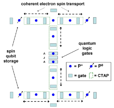
The 2D architecture introduced here requires relatively low gate densities and specifically address the problems listed above. In Fig. 1 the geometry is shown for the specific case of the exchange-interaction based Kane architecture. We note that the transport ideas presented here allow for a similar, but non-trivial development for the digital-Kane case. A buried array of ionised donors provide pathways for coherent transport of electron spins for in-plane horizontal and vertical shuttling (dashed-border sections) of qubit states into and out of the interaction zone. The overall gate density is low compared to the Kane case, and can be further reduced by increasing the transport pathway length (Fig. 2). Initially all gates inhibit tunnelling along any given channel. Coherent spin transport along one segment is achieved by adiabatically lowering the barriers in a well defined sequence to effect coherent transfer by adiabatic passage (CTAP) without populating the intervening channel donors GreentreeCTAP . We show that with appropriate donor separations, the shuttling time can be in the nanosecond range for one section. In Fig. 1 the coherent transport scheme is defined for the minimum number of donors. Higher order schemes with more donors reduces the gate density (see Fig. 2).
Logic gates are carried out in interaction zones distinct from qubit storage regions – shown in Fig. 1 are the cannonical A and J gates for electron spin based qubit control at the microsecond level Hill . After mandatory precision characterisation SchirmerOi ; Cole , interaction regions with unacceptably low couplings can be identified and bypassed in the circuit flow, thereby avoiding bottleneck issues arising from the sensitivity of the exchange interaction to donor placement. This design allows for new variations on the theme, e.g. digitisation of hyperfine control Skinner , or introduction of local buried B-field antennae structures LidarBwires , and space for SET readout techniques Kane ; LHFIR ; GreentreeTriple .
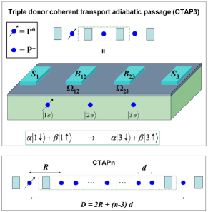
A schematic of the minimal three donor transport pathway is given in Fig. 2. The triple-well system , , () facilitates coherent state transport from to without populating the states. Techniques for coherent transfer by adiabatic passage are well known Vitanov , and for the donor system was proposed in GreentreeCTAP for the case of charge transfer. A superconducting version of the three state case has also been proposed Siewert . The system is controlled by shift gates, , which can modify the energy levels of the end donors, and barrier gates, which control the tunnelling rate between donors and .
Although the scheme we introduce here necessarily includes spin, we first consider the zero field case and ignore spin degrees of freedom GreentreeCTAP to illustrate the principles of CTAP in the one-electron three-donor system, 3D2+. The effective Hamiltonian for the 3D2+ system is:
| (1) |
where is the coherent tunnelling rate between donors and and . The eigenstates of (with energies and ) are
| (2) |
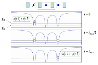
where we have introduced and . Transfer from state to is achieved by maintaining the system in state and changing the characteristics of adiabatically () from at to at by appropriate control of the tunnelling rates, without population leakage into the other eigenstates.
For the case of coherent spin transport we write the 3D2+ Hamiltonian in terms of spin/site operators as:
| (3) |
and numerically solve for the density matrix, , in the presence of a (dominant) charge dephasing rate , assumed to act equally on all coherences. Without attempting to fully optimize control we apply Gaussian pulses of the form , where and are the peak time and width of the control pulse modulating the tunnelling rate between position states and . To simplify matters for initial simulations we set the maximum tunnelling rates and standard deviations for each transition to be equal, i.e. and , and set (these conditions can be relaxed with no effect on the conclusions of this paper). Transfer is then optimized when the width of the pulses equals the time delay between the pulses Gaubatz . With total pulse time , we choose so that and . This ordering, where is applied before is known as the counter-intuitive pulse sequence and has significant advantages in improving transfer fidelity over other pulse sequences GreentreeCTAP . In Fig. 3 we present results showing transport using the counter-intuitive pulse ordering for a spin superposition (phases relative to the untransported state).
Generally, when the adiabaticity criterion is satisfied and the transport time is at least an order of magnitude faster than charge dephasing, the transport fidelity is high. These results are consistent with those of Ivanov et al Ivanov who considered the role of dephasing in three-state Stimulated Raman Adiabatic Passage (STIRAP). Although these competing timescales are essentially unmeasured at present, estimates Barrett ; Fedichkin for the P-P+ charge dephasing time are of order 10ns and a value of 220ns was reported recently for a Si:P double-dot Gorman , whereas sub-nanosecond tunnelling times are possible due to the strong confining potential of donor nuclei. The CTAP transport time will be defined primarily by the gate-assisted tunnelling rate, which we calculate as follows. Using the TCAD package we compute the potential due to a surface B-gate bias and determine the donor electron wave function in an effective mass basis, e.g. , about the six band minima where the are hydrogenic orbitals with Bohr radius , and . Diagonalising the total Hamiltonian of the system, using pseudopotentials to describe the silicon bandstructure, we obtain a generalised Kohn-Luttinger wave function:
| (4) |
where the Bloch states are . We form bonding and anti-bonding states , normalised by , and compute the gap as shown in Fig. 4 for basis sizes 55 and 140 ( = 5 and 7). Comparison of the non-linear regions indicates that the range of validity is 200 mV.
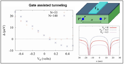
In contrast to what one expects for an isolated P-P+ system in vacuum where the nodal structure of the bonding and anti-bonding states is simple, the non-trivial nodal properties of the donor electron wave function and the proximity of the oxide interface complicates the tunnelling control. These calculations directly extend similar effects noted in the ungated P-P+ system Hu_Charge_Qubit . From Fig. 4 we see that for this configuration the tunnelling rate can be varied from zero at +100mV to 10 GHz at -200mV, giving a gate assisted tunnelling time of 60 ps.
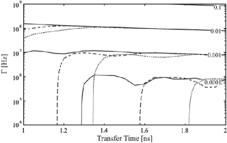
Based on this value, CTAP simulations for 5, 7 and 9 donor chains are presented in Fig. 5. The adiabatic nature of the transport scheme provides an inherent robustness, as evidenced in Fig. 5, which shows a remarkable uniformity in the response to charge dephasing for the different path lengths once the adiabatic regime is reached. Another consequence is that inevitable variations in tunnelling rates due to donor placement Hu_Charge_Qubit will not affect the viability of the scheme, as further simulations have explicitly verified. The extent to which controls the transport fidelity is also clear, although we note that there is room for improvement through optimisation of control pulses and minimisation of charge fluctuations through fabrication development. Non-zero transport errors may require monitoring mechanisms for heralding successful transport, or an error correction protocol for transport loss. As intrinsic spin-orbit coupling for donor states in silicon is very low, dephasing of donor electron spin is dominated by spectral diffusion due to spin impurities and is mitigated by isotopic purification DeSousa2 . For the bound state spin-orbit coupling, at mV we calculate from Eqn(4) the non-S components to be indicating that the deviation from the S sector is minimal. Together with the zero occupation of channel states, this suggests that charge dephasing will have a negligible second order effect on the spin coherence during transport. Decoupling of orbital and spin sectors has already given rise to demonstrations of coherent transport of electron spins over 100m Kikkawa .
The basic layout of 2D donor arrays, with storage regions, vertical and horizontal transport pathways and interaction zones, allows us to explicitly consider designs for fault-tolerant operation. For example, we can arrange the logical qubit groups and ancillas so that the transport rails allow for non-local intralogical qubit interactions (qubit – ancillas) and LNN interlogical interactions. With inherent parallelism of operation, interlogical gates can then be applied transversally as required to implement fault-tolerant gates. Another possibility with less stringent fabrication requirements is a linear qubit storage with transport and interaction rails either side.
The optimum arrangement for fault-tolerant operation requires sophisticated systems level simulations Copsey2 to determine the best use of this medium range quantum transport capability, and the corresponding improvements on the LNN threshold. In any case, it is clear that the introduction of coherent spin transport to donor quantum computing allows us to address many problems in the Kane concept, and consider scalable fault-tolerant architectures with low gate densities, room for SET structures and control, and a bypass mechanism for low value exchange gates. One expects the realities of the silicon crystaline environment will necessitate the characterisation of transport pathways, however, the precision requirements of the adiabatic CTAP mechanism would be far less than the quantum gate threshold.
We thank S. Das Sarma, G. Milburn, F. Wilhelm and J. Cole for comments, and support of the Australian Research Council, the U.S. National Security Agency, Advanced Research and Development Activity and Army Research Office under contract DAAD19-01-1-0653.
References
- (1) B.E. Kane, Nature 393, 133 (1998).
- (2) S. R. Schofield, et al Phys. Rev. Lett., 91, 136104 (2003).
- (3) D. N. Jamieson et al, Appl. Phys. Lett. 86, 202101 (2005)
- (4) R. Vrijen et al, Phys. Rev. A 62, 012306 (2000).
- (5) R. de Sousa, J. D. Delgado and S. Das Sarma, Phys. Rev. A 70, 052304 (2004).
- (6) C. Hill et al, quant-ph/0411104.
- (7) L.C.L. Hollenberg et al, Phys. Rev. B 69, 113301 (2004).
- (8) A. M. Tyryshkin et al, Phy. Rev. B68 193207 (2003).
- (9) R. Clark et al, Phil. Trans. Roy. Soc. Lond. A361, 1451 (2003).
- (10) T. Schenkel et al, J. Appl. Phys. 94, 7017 (2003).
- (11) T.M. Buehler et al, cond-mat/0506594.
- (12) A. Steane, in "Decoherence and its implications in quantum computation and information transfer", Gonis and Turchi, eds, pp.284-298 (IOS Press, Amsterdam, 2001).
- (13) D. Kielpinksy, C. Monroe and D.J. Wineland, Nature 417 709 (2002).
- (14) B. Koiller, X. Hu and S. Das Sarma, Phys. Rev. Lett 99 027903 (2002).
- (15) C.J. Wellard et al, Phys. Rev. B 68, 195209 (2003).
- (16) B.E. Kane, MRS Bulletin 30, 105 (2005).
- (17) M Oskin et al, Proceedings of ISCA 2003.
- (18) D. Copsey et al, IEEE Journal of Selected Topics in Quantum Electronics 9, 1552 (2003).
- (19) L.C.L. Hollenberg et al Phys. Rev. B 69, 233301 (2004).
- (20) T. Metodiev et al, 2nd Workshop on Non-Silicon Computation/30th International Symposium on Computer Architecture, Illinois, USA (2003).
- (21) D. Gottesman, J. Mod. Opt. 47, 333 (2000).
- (22) K.M. Svore et al, quant-ph/0410047.
- (23) A. Fowler, S. Devitt and L. Hollenberg, Quant. Inf. Comp. 4, 237-251 (2004).
- (24) S. Devitt, A. Fowler and L. Hollenberg, quant-ph/0408081
- (25) T. Szkopek et al, quant-ph/041111.
- (26) A.J. Skinner, M.E. Davenport, and B.E. Kane, Phys. Rev. Lett. 90, 087901 (2003).
- (27) A.D. Greentree et al, Phys. Rev B 70, 235317 (2004).
- (28) S.G. Schirmer, A. Kolli and D.K.L. Oi, Phys. Rev. A 69 050306 (2004).
- (29) J. Cole et al, Phys. Rev. A 71, 062312 (2005).
- (30) D.A. Lidar and J.H. Thywissen, J. Appl. Phys. 96, 754 (2004).
- (31) A.D. Greentree et al, Phys. Rev B 71, 113310 (2005).
- (32) N. V. Vitanov et al Ann. Rev. Phys. Chem. 52, 763 (2001).
- (33) J. Siewert and T. Brandes, Advances in Solid State Physics 44, 181 (2004).
- (34) U. Gaubatz, et al, J. Chem. Phys. 92, 5363 (1990).
- (35) P.A. Ivanov, N. V. Vitanov and K. Bergmanm, Phys. Rev. A 70, 063409 (2004).
- (36) S. Barrett and G.J. Milburn, Phys. Rev. B 68, 155307 (2003).
- (37) L. Fedichkin and A. Fedorov, Phys. Rev. A 69, 032311 (2004).
- (38) J. Gorman, D.G. Hasko, and D.A. Williams, cond-mat/0504451.
- (39) X. Hu, B. Koiller and S. Das Sarma, cond-mat/0412340
- (40) R. de Sousa and S. Das Sarma, Phys. Rev. B68, 115322 (2003).
- (41) J.M. Kikkawa and D.D. Awschalom, Nature 397 139 (1999).
- (42) D. Copsey et al, 2nd Workshop on Non-Silicon Computation/30th International Symposium on Computer Architecture, Illinois, USA (2003).