Corresponding author: J. Pomplun
URL: http://www.zib.de/nano-optics/
Email: pomplun@zib.de
Rigorous FEM-Simulation of EUV-Masks: Influence of Shape and Material Parameters
Abstract
We present rigorous simulations of EUV masks with technological imperfections like side-wall angles and corner roundings. We perform an optimization of two different geometrical parameters in order to fit the numerical results to results obtained from experimental scatterometry measurements. For the numerical simulations we use an adaptive finite element approach on irregular meshes [1]. This gives us the opportunity to model geometrical structures accurately. Moreover we comment on the use of domain decomposition techniques for EUV mask simulations [2]. Geometric mask parameters have a great influence on the diffraction pattern. We show that using accurate simulation tools it is possible to deduce the relevant geometrical parameters of EUV masks from scatterometry measurements.
This work results from a collaboration between AMTC (mask fabrication), Physikalisch-Technische Bundesanstalt (scatterometry) and ZIB/JCMwave (numerical simulation).
keywords:
EUV, mask, simulation, photolithography, FEMCopyright 2006 Society of Photo-Optical Instrumentation Engineers.
This paper has been published in Proc. SPIE 6349, 63493D
(2006),
(26th Annual BACUS Symposium on Photomask Technology,
P. M. Martin, R. J. Naber, Eds.)
and is made available
as an electronic reprint with permission of SPIE.
One print or electronic copy may be made for personal use only.
Systematic or multiple reproduction, distribution to multiple
locations via electronic or other means, duplication of any
material in this paper for a fee or for commercial purposes,
or modification of the content of the paper are prohibited.
1 Introduction
Extreme ultraviolet (EUV) lithography is considered as the main candidate for further miniaturization of computer technology. Since compared to state-of-the art photomasks, EUV masks are illuminated at oblique incidence, the quality of pattern profiles becomes important due to shadowing effects [3, 4]. Consequently, there is a need for adequate destruction free pattern profile metrology techniques, allowing characterization of mask features down to a typical size of nm.
Here we present an indirect method for the determination of geometrical EUV mask parameters [5]. Experimental scatterometry measurements are compared to numerical simulations of EUV masks using the finite element method (FEM).
2 Characterization of EUV masks by EUV scatterometry
Single wavelength scatterometry, the analysis of light diffracted from a periodic structure, is a well suited tool for analysis of the geometry of EUV masks. Since scatterometry only needs a light source and a simple detector with no imaging lens system, its setup is inexpensive and offers no additional technical challenges. Fig. 1(a) shows a sketch of the experimental setup. Light of fixed wavelength and fixed incident angle is reflected from the mask and the intensity of the reflected light is measured in dependence on the diffraction angle.
(a) (b)
\psfrag{euv}{light source}\psfrag{mult}{Mo/Si multilayer}\psfrag{det}{detector with slit}\psfrag{abs}{absorber stack}\psfrag{Si}{Si-cap}\psfrag{cd}{CD}\includegraphics[width=199.16928pt]{fig/scatter.eps}
\psfrag{euv}{light source}\psfrag{mult}{Mo/Si multilayer}\psfrag{det}{detector with slit}\psfrag{abs}{absorber stack}\psfrag{Si}{Si-cap}\psfrag{cd}{CD}\psfrag{diff}{diffraction angle [${}^{\circ}$]}\psfrag{intensity}{intensity [a.u.]}\includegraphics[width=199.16928pt]{fig/h4scatter.eps}
The use of EUV light for mask characterization is advantageous because it fits the small feature sizes on EUV masks. Diffraction phenomena are minimized, and of course the appropriate wavelength of the resonant structure of the underlying multilayer is chosen. Light is not only reflected at the top interface of the mask but all layers in the stack contribute to reflection. Therefore one expects that EUV radiation provides much more information on relevant EUV mask features than conventional long wavelength methods.
All measurements for the present work were performed by the Physikalisch-Technische Bundesanstalt (PTB) at the electron storage ring BESSY II [6]. PTB’s EUV reflectometer installed in the soft X-ray radiometry beamline allows high-accuracy measurements of very large samples with diameters up to mm [7, 8, 9].
3 FEM simulation of EUV scatterometry
Fig. 1(b) shows the result of a scatterometry measurement of an EUV test mask (see table 1) considered in the present work.
| Stack | Testmask |
|---|---|
| ARC + TaN-Absorber | nm |
| SiO2-Buffer | nm |
| Si-Capping layer | nm |
| Multilayer | Mo/Si |
| Design parameter | Testmask |
|---|---|
| Absorber stack sidewall angle | 90∘ |
| Pitch | 840nm |
| Top critical dimension | 140nm |
The position of the diffraction angles provide information about the pitch of the EUV absorber pattern. However the intensities of the diffraction orders do not carry direct information about other topological features of the mask. The determination of these features from a scatterometry measurement is a challenging inverse problem and a hot topic of actual research. Accurate and fast numerical simulation of the scattering experiment thereby plays a vital role. The FEM method is particularly suited for this application.
It has several advantages [10]:
-
•
Maxwell’s equations describing the scattering problem are solved rigorously without approximations.
-
•
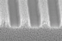
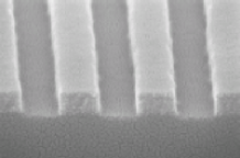
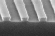
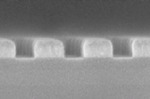
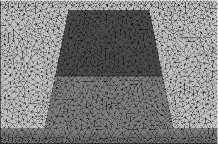
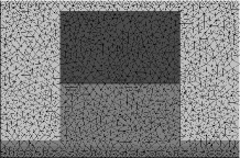
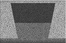
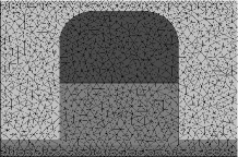
The flexibility of triangulations allows modeling of virtually arbitrary structures, as illustrated in Fig. 2.
-
•
Adaptive mesh-refinement strategies lead to very accurate results and small computational times which are crucial points for application of a numerical method to the characterization of EUV masks.
-
•
Choosing appropriate localized ansatz functions for the solution of Maxwell’s equations physical properties of the electric field like discontinuities or singularities can be modeled very accurately and don’t give rise to numerical problems, see Fig.3.
-
•
It is mathematically proven that the FEM approach converges with a fixed convergence rate towards the exact solution of Maxwell-type problems for decreasing mesh width of the triangulation. Therefore it is easy to check if numerical results can be trusted.
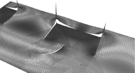
Throughout this paper we use the FEM solver JCMharmony for numerical solution of Maxwell’s equations. JCMharmony has been successfully applied to a wide range of electromagnetic field computations including waveguide structures [11], DUV phase masks [10], and other nano-structured materials [12, 13]. It provides higher order edge elements, multigrid methods, a-posteriori error control, adaptive mesh refinement, etc. Furthermore a special domain decomposition algorithm implemented in JCMharmony is utilized for simulation of EUV masks [2]. Light propagation in the multilayer stack beneath the absorber pattern can be determined analytically. The domain decomposition algorithm combines the analytical solution of the multilayer stack with the FEM solution of the absorber pattern, dramatically decreasing computational time and increasing accuracy of simulation results.
4 Determination of EUV mask parameters with FEM simulation
(a) (b)
The idea of characterising EUV masks with scatterometry measurements and FEM simulations is the comparison of the intensities of experimental diffraction orders with numerically obtained results [5]. First the geometry of the EUV mask is modeled using a finite number of parameters. Then scattering from the EUV mask is simulated and the intensities of the diffraction orders are computed. The deviation between experimental and numerical intensities is computed and the parameters which minimize this deviation determined. This leads to a finite dimensional optimization problem. In the experimental setup light of each diffraction order is always reflected into a finite solid angle leading to peaks with finite width, see Fig. 1(b). The experimental intensities that are used are given as the heights of these peaks which are only proportional to the whole intensity diffracted into an order (i.e. the integral over a peak). Numerically we determine the whole intensity of each diffraction order and therefore we have to scale the simulated intensities uniformly with a factor before determining the deviation :
| (1) |
where the global scaling factor is determined by minimizing with respect to :
| (2) |
The described procedure was applied to an EUV test mask produced by AMTC. The unknown mask parameters of interest were the sidewall angle of the absorber stack (which was restricted to ) and the top critical dimension (defined in Fig. 4).
The search for the optimal parameter set of the layout was performed using the Nelder-Mead simplex algorithm. As starting point the AMTC design parameters were chosen. In order to evaluate the results of our procedure scatterometry measurements and FEM simulations were compared at three different EUV wavelengths, shown in Fig. 5.
A comparison of diffraction orders obtained from scatterometry and FEM simulation is shown in Fig. 7 for the optimal EUV mask parameters found during optimization. We see excellent agreement at all wavelengths of incident EUV radiation. Only the tenth diffraction order at nm differs. Here the simulated intensity is much lower than the experimental and therefore the deviation much larger than for nm and nm, see table 2.
(a) (b) (c)
\psfrag{xi}{$\xi^{2}$}\psfrag{angle}{absorber angle $\alpha$ [${}^{\circ}$]}\psfrag{width}{top CD [nm]}\psfrag{radius}{edge Radius R [nm]}\includegraphics[width=145.10922pt,height=122.34692pt]{fig/width.eps} \psfrag{xi}{$\xi^{2}$}\psfrag{angle}{absorber angle $\alpha$ [${}^{\circ}$]}\psfrag{width}{top CD [nm]}\psfrag{radius}{edge Radius R [nm]}\includegraphics[width=145.10922pt,height=122.34692pt]{fig/angle.eps} \psfrag{xi}{$\xi^{2}$}\psfrag{angle}{absorber angle $\alpha$ [${}^{\circ}$]}\psfrag{width}{top CD [nm]}\psfrag{radius}{edge Radius R [nm]}\includegraphics[width=145.10922pt,height=122.34692pt]{fig/corner.eps}
nm
\psfrag{diffraction}{diffraction order}\psfrag{int}{intensity [a.u.]}\psfrag{exp}{experimental}\psfrag{sim}{FEM computation}\includegraphics[width=227.62204pt]{fig/scatt134.eps}
nm
\psfrag{diffraction}{diffraction order}\psfrag{int}{intensity [a.u.]}\psfrag{exp}{experimental}\psfrag{sim}{FEM computation}\includegraphics[width=227.62204pt]{fig/scatt1365.eps}
nm
\psfrag{diffraction}{diffraction order}\psfrag{int}{intensity [a.u.]}\psfrag{exp}{experimental}\psfrag{sim}{FEM computation}\includegraphics[width=227.62204pt]{fig/scatt139.eps}
The geometrical parameters which belong to the best fitting simulations are shown in table 2 in comparison to the desired design values for the mask.
| geometrical parameter | design value | FEM nm | FEM nm | FEM nm |
|---|---|---|---|---|
| [∘] | 90 | 87.9 | 90.0 | 90.0 |
| top CD [nm] | 140 | 145.7 | 146.5 | 146.5 |
| deviation | 0.18 | 0.24 | 1.32 |
We see that the best fitting geometries agree extremely well for nm and nm. For nm the absorber angle is (2.2%) smaller and the top CD is nm (0.5%) smaller than for and .
Fig. 6(a), (b) shows how the deviation between experimental and simulated diffraction orders depends on the top critical dimension and the absorber angle . It grows strongly with increasing distance from the optimal geometrical parameters. This shows that the presented method is very robust.
As a further geometrical parameter the absorber edge radius was considered, see Fig. 4(b). The best fitting value for was determined at the incident wavelength nm and the optimal values for top CD = nm and . Fig. 6(c) shows a minimal deviation between experiment and simulation for nm. We see that the edge radius does not have such a great effect on the diffraction orders since the deviation hardly changes compared to the effects of the top CD (a) and absorber angle (b). This confirms further that for the determination of more sophisticated geometrical parameters very accurate simulations are crucial. As already mentioned the convergence of the FEM method is mathematically proven and it is therefore a very good choice for the presented method. Fig. 8 shows the convergence of the zeroth and first diffraction order. We see the relative error in dependence on the number of unknowns of the FEM computation (i.e. a coarser triangulation). Furthermore the computational time on a standard PC (GHz Intel Pentium 4, 1GB RAM) is shown at each refinement step of the grid. After s we already have a relative error of much smaller than the experimental uncertainty of about . A short computation time also becomes crucial for the determination of mask parameters when choosing a larger number of independent geometrical parameters and performing the search for the optimal values in a higher dimensional space. We expect that scatterometry measurements at several different wavelengths will become very important for the presented method when characterizing EUV masks in greater detail. In order to further validate the geometrical parameters of the EUV mask obtained via scatterometry and FEM simulation a comparison to direct measurements like atomic force microscopy is planned. These measurements will be carried out at AMTC.
5 Conclusions
We demonstrated that single wavelength scatterometry in combination with FEM simulations is a promising candidate for an accurate and robust destruction free characterization of EUV masks. Thereby experimental diffraction orders are compared to FEM simulations of EUV masks. For FEM simulations the EUV mask is first described with a finite number of geometrical parameters like sidewall angles, line widths, corner roundings, etc. and then the best fitting values determined by minimizing the deviation of experimental and numerical data.
Here we considered the top critical dimension, the sidewall angle and the edge radius of the absorber stack of an EUV mask as unknown geometrical parameters. The search for the best fitting geometry at three different wavelengths gave nearly the same values for the top critical dimension and the absorber sidewall angle proving both robustness and accuracy of the method. Furthermore the absorber edge radius had only minor influence on the numerical diffraction pattern.
We showed that very accurate numerical simulations are crucial for detailed geometric characterization of EUV masks using scatterometry data. The FEM method is well suited for the simulation of EUV masks since it allows computation of nearly arbitrary geometries, is very accurate and very fast. Thereby very fast simulation of the EUV mask with a fixed parameter set provides a precondition for the solution of the given inverse problem.
References
- [1] S. Burger, L. Zschiedrich, R. Klose, A. Schädle, F. Schmidt, C. Enkrich, S. Linden, M. Wegener, and C. M. Soukoulis, “Numerical investigation of light scattering off split-ring resonators,” in Metamaterials, T. Szoplik, E. Özbay, C. M. Soukoulis, and N. I. Zheludev, eds., 5955, pp. 18–26, Proc. SPIE, 2005.
- [2] L. Zschiedrich, S. Burger, A. Schädle, and F. Schmidt, “Domain decomposition method for electromagnetic scattering problems,” in Proceedings of the 5th International Conference on Numerical Simulation of Optoelectronic devices, pp. 55–56, 2005.
- [3] M. Sugawara, I. Nishiyama, and M. Takai, “Influence of asymmetry of diffracted light on printability in EUV lithography,” 5751, pp. 721–732, Proc. SPIE, 2005.
- [4] M. Sugawara and I. Nishiyama, “Impact of slanted absorber sidewall on printability in EUV lithography,” 5992, Proc. SPIE, 2005.
- [5] J. Perlich, F.-M. Kamm, J. Rau, F. Scholze, and G.Ulm, “Characterization of extreme ultraviolet masks by extreme ultraviolet scatterometry,” J. Vac. Sci. Technol. B 22, pp. 3059–3062, 2004.
- [6] G. Ulm, B. Beckhoff, R. Klein, M. Krumrey, H. Rabus, and R. Thornagel, “The PTB radiometry laboratory at the BESSY II electron storage ring,” 3444, pp. 610–621, Proc. SPIE, 1998.
- [7] J. Tümmler, G. Brandt, J. Eden, H. Scherr, F. Scholze, and G. Ulm, “Characterization of the PTB EUV reflectometry facility for large EUVL optical components,” 5037, pp. 265–273, Proc. SPIE, 2003.
- [8] F. Scholze, C. Laubis, C. Buchholz, A. Fischer, S. Plöger, F. Scholz, H. Wagner, and G. Ulm, “Status of EUV reflectometry at PTB,” 5751, pp. 749–758, Proc. SPIE, 2005.
- [9] F. Scholze, J. Tümmler, and G. Ulm, “High-accuracy radiometry in the EUV range at the PTB soft X-ray radiometry beamline,” 40, pp. 224–228, Metrologia, 2003.
- [10] S. Burger, R. Köhle, L. Zschiedrich, W. Gao, F. Schmidt, R. März, and C. Nölscher, “Benchmark of fem, waveguide and fdtd algorithms for rigorous mask simulation,” in Photomask Technology, J. T. Weed and P. M. Martin, eds., 5992, pp. 378–389, Proc. SPIE, 2005.
- [11] S. Burger, R. Klose, A. Schädle, and F. S. and L. Zschiedrich, “Fem modelling of 3d photonic crystals and photonic crystal waveguides,” in Integrated Optics: Devices, Materials, and Technologies IX, Y. Sidorin and C. A. Wächter, eds., 5728, pp. 164–173, Proc. SPIE, 2005.
- [12] C. Enkrich, M. Wegener, S. Linden, S. Burger, L. Zschiedrich, F. Schmidt, C. Zhou, T. Koschny, and C. M. Soukoulis, “Magnetic metamaterials at telecommunication and visible frequencies,” Phys. Rev. Lett. 95, p. 203901, 2005.
- [13] T. Kalkbrenner, U. Hakanson, A. Schädle, S. Burger, C. Henkel, and V. Sandoghdar, “Optical microscopy using the spectral modifications of a nano-antenna,” Phys. Rev. Lett. 95, p. 200801, 2005.