Low flicker-noise DC amplifier for 50 sources
E. Rubiola, F. Lardet-Vieudrin, “Low flicker-noise amplifier for 50 sources”, Review of Scientific Instruments vol. 75 no. 5 pp.1323–1326, May 2004)
Abstract
This article analyzes the design of a low-noise amplifier intended as the input front-end for the measurement of the low-frequency components (below 10 Hz) of a 50 source. Low residual flicker is the main desired performance. This feature can only be appreciated if white noise is sufficiently low, and if an appropriate design ensures dc stability. An optimal solution is proposed, in which the low-noise and dc-stability features are achieved at a reasonable complexity. Gain is accurate to more than 100 kHz, which makes the amplifier an appealing external front-end for fast Fourier transform (FFT) analyzers.
1 Introduction
Often the experimentalist needs a low-noise preamplifier for the analysis of low-frequency components (below 10 Hz) from a 50 source. The desired amplifier chiefly exhibits low residual flicker and high thermal stability, besides low white noise. Thermal stability without need for temperature control is a desirable feature. In fact the problem with temperature control, worse than complexity, is that in a nonstabilized environment thermal gradients fluctuate, and in turn low-frequency noise is taken in. A low-noise amplifier may be regarded as an old subject, nonetheless innovation in analysis methods and in available parts provides insight and new design. The application we initially had in mind is the postdetection preamplifier for phase noise measurements [RG02]. Yet, there resulted a versatile general-purpose scheme useful in experimental electronics and physics.
2 Design Strategy
The choice of the input stage determines the success of a precision amplifier. This issue involves the choice of appropriate devices and of the topology.
Available low-noise devices are the junction field-effect transistor (JFET) and the bipolar transistor (BJT), either as part of an operational amplifier or as a stand-alone component. The white noise of these devices is well understood [vdZ86, vdZ59, Net81, Erd81]. Conversely, flicker noise is still elusive and relies upon models, the most accredited of which are due to McWhorter [McW57] and Hooge [Hoo69], or on smart narrow-domain analyses, like [GJ85a, GJ85b, MJ99], rather than on a unified theory. Even worse, aging and thermal drift chiefly depend on proprietary technologies, thus scientific literature ends up to be of scarce usefulness. The JFET is appealing because of the inherently low white noise. The noise temperature can be as low as a fraction of a degree Kelvin. Unfortunately, the low noise of the JFET derives from low input current, hence a high input resistance (some M) is necessary. The JFET noise voltage is hardly lower than 5 , some five to six times higher than the thermal noise of a 50 resistor ( ). The JFET is therefore discarded in favor of the BJT.
A feedback scheme, in which the gain is determined by a resistive network, is necessary for gain accuracy and flatness over frequency. Besides the well known differential stage, a single-transistor configuration is possible (Ref. [MF73], page 123), in which the input is connected to the base and the feedback to the emitter. This configuration was popular in early audio hi-fi amplifiers. The advantage of the single-transistor scheme is that noise power is half the noise of a differential stage. On the other hand, in a dc-coupled circuit thermal effects are difficult to compensate without reintroducing noise, while thermal compensation of the differential stage is guaranteed by the symmetry of the base-emitter junctions. Hence we opt for the differential pair.
| OP27111Low-noise operational amplifier. | LT1028111Low-noise operational amplifier. | MAT02222Matched-transistor pair. MAT02 is npn, MAT03 is pnp. Data refer to the pair, biased at mA. | MAT03222Matched-transistor pair. MAT02 is npn, MAT03 is pnp. Data refer to the pair, biased at mA. | unit |
MAT03
measured333Some MAT03 samples measured in our laboratory. See Sec. 3 |
|
| WHITE NOISE | ||||||
| noise voltage444Power-law model of the spectrum, voltage or current, | 3 | 0.9 | 0.9 | 0.7 | 0.8 | |
| noise current444Power-law model of the spectrum, voltage or current, | 0.4 | 1 | 0.9 | 1.4 555Obtained from the total noise with 100 k input resistance. | 1.2 | |
| noise power | ||||||
| noise temperature | 174 | 130 | 117 | 142 | K | 139 |
| optimum resistance | 7500 | 900 | 1000 | 500 | 667 | |
| -input noise | 3.3 | 1.55 | 1.55 | 1.5 | 1.5 666Measured on the complete amplifier (Sec. 4), independently of the measurement of the above and . | |
| FLICKER NOISE | ||||||
| noise voltage444Power-law model of the spectrum, voltage or current, | 4.3 | 1.7 | 1.6 | 1.2 | ( )777Derives from the noise current through . See Sec. 4. | |
| noise current444Power-law model of the spectrum, voltage or current, | 4.7 | 16 | 1.6 | n. a. | 11 | |
| noise power | – | (…)888Can not be compared to other data because voltage and current are correlated. See Sec. 4. | ||||
| 1-Hz noise temperature | 2950 | 3850 | 370 | – | K | (…)888Can not be compared to other data because voltage and current are correlated. See Sec. 4. |
| optimum resistance | 910 | 106 | 1000 | – | (…)888Can not be compared to other data because voltage and current are correlated. See Sec. 4. | |
| -input noise | 4.3 | 2.3 | 1.6 | – | 1.1 666Measured on the complete amplifier (Sec. 4), independently of the measurement of the above and . | |
| THERMAL DRIFT | 200 | 250 | 100 | 300 | nV/K | – |
Table 1 compares a selection of low-noise bipolar amplifiers. The first columns are based on the specifications available on the web sites [ana, lin]. The right-hand column derives from our measurements, discussed in Secs. 3 and 4. Noise is described in terms of a pair of random sources, voltage and current, which are assumed independent. This refers to the Rothe-Dahlke model [RD56]. Nonetheless, a correlation factor arises in measurements, due to the distributed base resistance . Whether and how is accounted for in the specifications is often unclear. The noise spectra are approximated with the power law . This model, commonly used in the domain of time and frequency, fits to the observations and provides simple rules of transformation of spectra into two-sample (Allan) variance . This variance is an effective way to describe the stability of a quantity as a function of the measurement time , avoiding the divergence problem of the processes in which . References [Rut78] and [RFD01] provide the background on this subject, and application to operational amplifiers.
The noise power spectrum is the minimum noise of the device, i.e., the noise that we expect when the input is connected to a cold (0 K) resistor of value , still under the assumption that voltage and current are uncorrelated. When the input resistance takes the optimum value , voltage and current contributions to noise are equal. The optimum resistance is for white noise and for flicker. Denoting by the corner frequency at which flicker noise is equal to white noise, thus for voltage and for current, it holds that . Interestingly, with most bipolar operational amplifiers we find , hence . Whereas we have no explanation for this result, the lower value of the flicker optimum resistance is a fortunate outcome. The equivalent temperature is the noise power spectrum divided by the Boltzmann constant J/K. A crucial parameter of Table 1 is the total noise when each input is connected to a 50 resistor at room temperature. This calculated value includes noise voltage and current, and the thermal noise of the two resistors. In a complete amplifier two resistors are needed, at the input and in the feedback circuit.
Still from Table 1, the transistor pairs show lower noise than the operational amplifiers, although the PNP pair is only partially documented. Experience indicates that PNP transistors are not as good as NPN ones to most extents, but exhibit lower noise. In other domains, frequency multipliers and radio-frequency oscillators make use of PNP transistors for critical application because of the lower flicker noise. Encouraged by this fact, we tried a differential amplifier design based on the MAT03, after independent measurement of some samples.
3 Input Stage

The typical noise spectrum of the MAT03, reported in the data sheet, shows an anomalous slope at low frequencies (0.1–1 Hz), significantly different from . This is particularly visible at low collector current (10–100 A), but also noticeable at mA. We suspect that the typical spectrum reflects the temperature fluctuation of the environment through the temperature coefficient of the offset voltage rather than providing information on the flicker noise inherent in the transistor pair. The measurement of a spectrum from 0.1 Hz takes some 5 min. At that time scale, in a normal laboratory environment the dominant fluctuation is a drift. If the drift is linear, starting at , the Fourier transform is . Dropping off the term , which is a dc term not visible in a log-log scale, the power spectrum density, i.e., the squared Fourier transform, is
| (1) |
A parabolic drift—seldom encountered in practice—has a spectrum proportional to , while a smoothly walking drift tends to be of the type. As a consequence, a thermal drift can be mistaken for a random process of slope to , which may hide the inherent noise of the device. For this reason, the test circuit (Fig. 1) must be enclosed in an appropriate environment. We used, with similar results, a Dewar flask coupled to the environment via a heat exchanger, and a metal box mounted on a heat sink that has a mass of 1 kg and a thermal resistance of 0.6 K/W. These odd layouts provide passive temperature stabilization through a time constant and by eliminating convection, and evacuate the small amount of heat (200 mW) dissipated by the circuit.

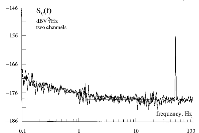
Due to the low value of (15–20 ) the current measurement can be made independent of voltage noise, but not vice versa. Thus, we first measure the noise current setting k, which is limited by the offset current; then we measure the noise voltage setting . A technical difficulty is that at 1 Hz and below most spectrum analyzers—including our one—must be coupled in dc, hence high offset stability is needed in order to prevent saturation of the analyzer. The measured spectra are (i.e., 1.2 white, and 11 flicker), and (i.e., 1 white, and 425 flicker). The current spectrum is the inherent noise current of the differential pair. Conversely, with the voltage spectrum (Fig. 2) we must account for the effect of and . With our test circuit, the expected white noise is , which is the sum of thermal noise and the shot noise of the base current . is the equivalent base resistance, while the shot noise of the collector current is neglected. Assuming (from the data sheet), the estimated noise is . This is in agreement with the measured value of . Then, we observe the effect of the current flickering on the test circuit is . The latter is close to the measured value . Hence, the observed voltage flickering derives from the current noise through the external resistors and the internal distributed resistance of the transistors. Voltage and current are therefore highly correlated. As a further consequence, the product is not the minimum noise power, and the ratio is not the optimum resistance. The corresponding places in Table 1 are left blank. Due to the measurement uncertainty, we can only state that a true independent voltage flickering, if any, is not greater than . The same uncertainty affects the optimum resistance , which is close to zero.
The measured white noise is in agreement with the data sheet. On the other hand, our measurements of flicker noise are made in such unusual conditions that the results should not be considered in contradiction with the specifications, as the specifications reflect the the low-frequency behavior of the device in a normal environment.
4 Implementation and Results

Figure 3 shows the scheme of the complete amplifier, inspired to the “super low-noise amplifier” proposed in Fig. 3a of the MAT03 data sheet. The NPN version is also discussed in Ref. [Fra97] (p. 344). The original circuit makes use of three differential pairs connected in parallel, as it is designed for the lowest white noise with low impedance sources ( ), like coil microphones. In our case, using more than one differential pair would increase the flicker because of current noise.
The collector current mA results as a trade-off between white noise, which is lower at high , dc stability, which is better at low dissipated power, flicker, and practical convenience. The gain of the differential pair is , where mA/V is the transistor transconductance, and k is the collector resistance. The overall gain is . Hence the gain of the OP27 is of 2.5, which guarantees the closed-loop stability (here, oscillation-free operation). If a lower gain is needed, the gain of the differential stage must be lowered by inserting . The trick is that the midpoint of is a ground for the dynamic signal, hence the equivalent collector resistance that sets the gain is in parallel to . The bias current source is a cascode Wilson scheme, which includes a light emitting diode (LED) that provides some temperature compensation.
The stability of the collector resistors is a crucial point because the voltage across them is of 5 V. If each of these resistors has a temperature coefficient of /K, in the worst case there results a temperature coefficient of 10 V/K at the differential output, which is equivalent to an input thermal drift of 50 nV/K. This is 1/6 of the thermal coefficient of the differential pair. In addition, absolute accuracy is important in order to match the collector currents. This is necessary to take the full benefit from the symmetry of the transistor pair.

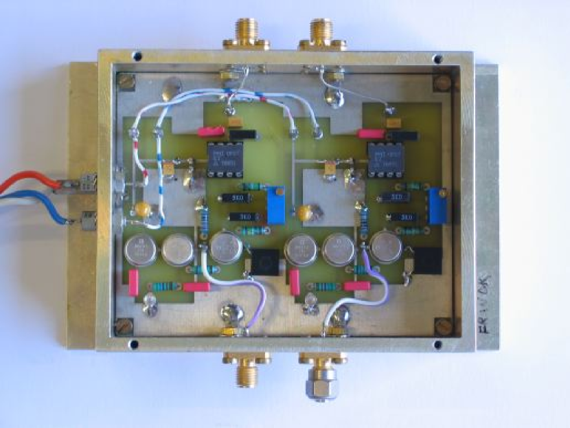
Two equal amplifiers are assembled on a printed circuit board, and inserted in a , 4 mm thick aluminum box (Fig. 4). The box provides thermal coupling to the environment with a suitable time constant, and prevents fluctuations due to convection. filters, of the type commonly used in HF/VHF circuits, are inserted in series to the power supply, in addition to the usual bypass capacitors. For best stability, and also for mechanical compatibility with our equipment, input and output connector are of the SMA type. Input cables should not PTFE-insulated because of piezoelectricity (see the review paper [Fuk00]).

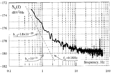
Figure 5 shows the noise spectrum of one prototype input terminated to a 50 resistor. The measured noise is (white) and (flicker). The corner frequency at which the white and flicker noise are equal is Hz. Converting the flicker noise into two-sample (Allan) deviation, we get nV, independent of the measurement time .
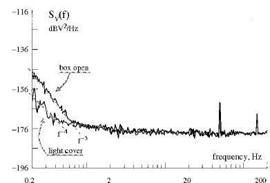
Finally, we made a simple experiment aimed to explain in practical terms the importance of a proper mechanical assembly. We first removed the Al cover, exposing the circuit to the air flow of the room, yet in a quiet environment, far from doors, fans, etc., and then we replaced the cover with a sheet of plain paper (80 ). The low-frequency spectrum (Fig. 6) is in the first case, and about in the second case. This indicates the presence of an irregular drift, smoothed by the paper protection. Interestingly, Hashiguchi [SHOT04] reports on thermal effects with the same slope and similar cutoff frequencies, observed on a low-noise JFET amplifier for high impedance sources.

References
- [ana] http://www.analog.com/.
- [Erd81] George Erdi, Amplifier techniques for combining low noise, precision, and high-speed performance, IEEE J. Solid-State Circuits 16 (1981), no. 6, 653–661.
- [Fra97] Sergio Franco, Design with operational amplifiers and analog integrated circuits, 2nd ed., McGraw Hill, Singapore, 1997.
- [Fuk00] Eiichi Fukada, History and recent progress in piezoelectric polymers, IEEE Trans. Ultras. Ferroel. and Freq. Contr. 47 (2000), no. 6, 1277–1290.
- [GJ85a] C. T. Green and B. K. Jones, noise in bipolar transistors, J. Phys. D: Appl. Phys. 18 (1985), 77–91.
- [GJ85b] , Correlation between noise and dc characteristics in bipolar transistors, J. Phys. D: Appl. Phys. 18 (1985), 2269–275.
- [Hoo69] Friits N. Hooge, noise is no surface effect, Phys. Lett. A 29 (1969), 139–140.
- [lin] http://www.linear.com/.
- [McW57] A. L. McWhorter, noise and germanium surface properties, Semiconductor Surface Physics (R. H. Kingston, ed.), University of Pennsylvania Press, Philadelphia, 1957, pp. 207–228.
- [MF73] C. D. Motchenbacher and F. C. Fitchen, Low-noise electronic design, 1st ed., John Wiley, New York, 1973.
- [MJ99] M. Schroter M. Jamal Deen, S. L. Rumuantsev, The origin of noise in polysilicon emitter bipolar transistors, J. Appl. Phys. 85 (1999), no. 2, 1192–1195.
- [Net81] Yishay Netzer, The design of low-noise amplifiers, Proc. IEEE 69 (1981), no. 6, 728–742.
- [RD56] H. Rothe and W. Dahlke, Theory of noisy fourpoles, Proc. IRE 44 (1956), 811–818.
- [RFD01] Enrico Rubiola, Claudio Francese, and Andrea De Marchi, Long term behavior of operational amplifiers, IEEE Trans. Instrum. Meas. 50 (2001), no. 1, 89–94.
- [RG02] Enrico Rubiola and Vincent Giordano, Advanced interferometric phase and amplitude noise measurements, Rev. Sci. Instrum. 73 (2002), no. 6, 2445–2457.
- [Rut78] Jacques Rutman, Characterization of phase and frequency instabilities in precision frequency sources: Fifteen years of progress, Proc. IEEE 66 (1978), no. 9, 1048–1075.
- [SHOT04] Josef Sikula, Sumihisa Hashiguchi, Makoto Ohki, and Munecazu Tacano, Some considerations for the construction of low-noise amplifiers in very low frequency region, Advanced Experimental Methods in Noise Research on Nanoscale Electronic Devices (Josef Sikula and Michael Levinsthein, eds.), Kluwer, 2004, pp. 237–244.
- [vdZ59] Aldert van der Ziel, Fluctuation phenomena in semi-conductors, Butterworths, London, 1959.
- [vdZ86] , Noise in solid state devices and circuits, Wiley, New York, 1986.