A CCD Vertex Detector for a High-Energy Linear e+e-Collider
Abstract
I present a summary of the experience with CCD-based vertex detectors at the SLD experiment at SLAC, and discuss their advantages for use at a future high-energy linear e+e-collider. The extensive R&D programme to improve further the vertexing capabilities of CCD detectors is also outlined.
OUNP-99-10
August 2 1999
email: p.burrows1@physics.ox.ac.uk
Presented at Vertex99, Texel
The Netherlands, 20-25 June 1999
1 Introduction to CCDs
Charge-coupled devices (CCDs) were originally applied in high-energy particle physics at a fixed-target charm-production experiment, and their utility for high-precision vertexing of short-lived particles was quickly realised [1]. More recently two generations of CCD vertex detectors (VXDs) were used in the e+e-colliding-beam environment of the SLD experiment at the first linear collider, SLC, at SLAC.
CCDs are silicon pixel devices which are widely used for imaging; one common application is in home video cameras, and there is extensive industrial manufacturing experience in Europe, Japan and the US. CCDs can be made with high pixel granularity. For example, those used at SLD comprise 2020 m2 pixels, offering the possibility of intrinsic space-point resolution of better than 4 m, determined from the centroid of the small number of pixels which are hit when a charged particle traverses the device. The active depth in the silicon is only 20 m, so each pixel is effectively a cube of side 20 m, yielding true 3-dimensional spatial information. Furthermore, this small active depth allows CCDs to be made very thin, ultimately perhaps as thin as 20 m, which corresponds to less than 0.1% of a radiation length (), and yields a very small multiple scattering of charged particles. Also, large-area CCDs can be made for scientific purposes, allowing an elegant VXD geometry with very few (if any) cracks or gaps for readout cables or support structures. For example, the second-generation CCDs used at SLD were of size 80 16 mm2.
The combination of superb spatial resolution, low multiple scattering, and large-area devices, with a decade of operating experience at the first linear collider, SLC, hence makes CCDs a very attractive option for use in a vertex detector at a second-generation linear collider (LC). Such colliders are being actively pursued by consortia centred around SLAC and KEK (NLC/JLC), DESY (TESLA) and CERN (CLIC).
In Section 2 I review briefly the SLD CCD VXD experience; more details are given in a complementary presentation [2]. In Section 3 I discuss the physics requirements for the LC VXD. In Section 4 I present the current conceptual design, and the simulated flavour-tagging performance. The R&D programme that is underway to achieve these goals is described in Section 5. In Section 6 I give a brief summary and outlook.
2 SLD CCD VXD Experience
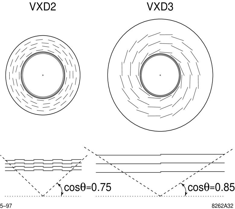
The SLD experiment has utilised three CCD arrays for heavy-flavour tagging in decays. In 1991 a 3-ladder prototype detector, VXD1, was installed for initial operating experience. In 1992 a complete four-layer vertex detector, VXD2, was installed and operated until 1995. VXD2 [3] utilised 64 ladders arranged in 4 incomplete azimuthal layers (Fig. 1). Due to the incomplete coverage a track at a polar angle of 90∘ to the beamline passed through, on average, only 2.3 layers, and 2-hit coverage extended down to polar angles within . The device contained a total of 512 roughly cm2 CCDs, giving a total of 120M pixels.
In 1996 a brand new detector, VXD3 [4], was installed that capitalised on improvements in CCD technology since VXD2 was originally designed. The main improvement was to utilise much larger, cm2, and thinner ( 3) CCDs, which allowed a significantly improved geometry (Fig 1). Ladders were formed from two CCDs placed end-to-end (with a small overlap in coverage) on opposite sides of a beryllium support beam, and arranged in 3 complete azimuthal layers, with a ‘shingled’ geometry to ensure no gaps in azimuth. A much better acceptance of (3 hits) and (2 hits) was achieved with these longer ladders. 96 CCDS were used, giving a total count of 307M pixels.

In operations from 1996 through 1998 VXD3 performed beautifully, yielding a measured single-hit resolution of 3.8 m, and a track impact-parameter resolution of 7.8 m (9.7 m) in () respectively, measured using 46 GeV tracks in events. The multiple scattering term was found to be m. The measured precision on the position of the micron-sized (mm-long) SLC interaction point (IP) was found to be 3 m in (30 m in ) respectively. As an illustration of the vertexing performance, the resolution on the decay-length of mesons w.r.t. the IP was estimated to be characterised by a double-Gaussian function with widths of 46 m, representing 60% of the population, and 158m representing the remainder, which is outstanding compared with other e+e-experiments. For inclusive -hemisphere tagging a sample purity of 98% can be obtained with a tag efficiency of up to 45%, and for inclusive -tagging a sample purity of around 70% can be obtained with a tag efficiency of up to 20%. Again, this performance is unsurpassed by other experiments.
It is worth noting several important lessons learned from the SLD VXD3 experience:
-
•
The intrinsic spatial resolution of 6 m, which one would naively estimate for a pixel size of 20 m, was significantly improved to better than 4 m by capitalising on the charge-sharing between several pixels and performing cluster centroid-finding.
-
•
The complete 3-layer coverage for allowed vector hits to be found within the VXD alone, which could then be included at an earlier stage of the track-finding algorithm, allowing a ‘pointing out’ rather than ‘pointing in’ approach to track-linking with the main tracking chamber. One (or two) VXD hits were also included in the track-finding of low polar-angle events, yielding an improved acceptance and significantly better momentum determination.
-
•
Even though in each triggered event there were, on average, roughly 15,000 pixels hit by background particles from SLC, the large pixellation of VXD3 ensured that the occupancy was approximately , yielding essentially zero confusion between bonafidehits on tracks and background hits.
-
•
The long readout time of VXD3, around 180 ms, did not lead to any deadtime at all. If a second trigger was taken during the readout period of the previously triggered event, the VXD readout was simply restarted and two ‘overlapping frames’ were recorded. The low hit density ensured that there was zero confusion of hits between the two overlapping events.
-
•
Despite the VXD3 ladders being very thin, roughly 0.4% , multiple scattering dominated the impact-parameter resolution for tracks with momenta less than 3 GeV/, i.e.the vast majority of tracks in decays.
These lessons have proven invaluable for consideration of the design of a VXD for the future LC.
3 Linear Collider Physics Demands
The second-generation linear collider will probably be built to operate at c.m. energies in the range between the current LEP2 energy of around 200 GeV and up to around 0.8 - 1 TeV. The strategy for choosing the energy steps will be developed as we learn more about the Higgs boson(s) and beyond-Standard-Model particles from searches at LEP2, the Tevatron, HERA and the LHC. Consideration of a high-statistics run at the resonance, for super-precise measurements of electroweak parameters, is also under discussion.
Many of the interesting physics processes can be characterised as multijet final states containing heavy-flavour jets. Some representative examples are:
1) e+e-
2) e+e-
3) e+e-
4) e+e-
5) e+e-
6) e+e-
7) e+e-
It should be noted that charm- and -tagging, as well as -tagging, will be very important. For example, measurements of the branching ratios for (the) Higgs boson(s) to decay into , , and pairs (examples 1-3) (and/or , and pairs for a heavy Higgs) will be crucial to map out the mass-dependence of the Higgs coupling and to determine the nature (SM, MSSM, SUGRA ) of the Higgs particle(s).
Example 4 could yield a 6-jet final state containing 2 -jets. Example 5 could yield a 12-jet final state containing 4 -jets. Example 6 comprises 2 charm jets + missing energy in the final state. Example 7 could yield an 8-jet final state containing 4 -jets.
Because of this multijet structure, even at = 1 TeV many of these processes will have jet energies in the range 50 200 GeV, which is not significantly larger than at SLC, LEP or LEP2. The track momenta will be correspondingly low. For example, at = 500 GeV the mean track momentum in e+e- events is expected to be around 2 GeV/, so that with the current SLD VXD3 multiple scattering would limit the impact-parameter resolution for the majority of tracks!
Furthermore, some of these processes may lie close to the boundary of the accessible phase space, suggesting that extremely high flavour-tagging efficiency will be crucial for identifying a potentially small sample of events above a large multijet combinatorial background. It is worth bearing in mind that a doubling of the single-jet tagging efficiency at high purity is equivalent to a luminosity gain of a factor of 16 for a 4-jet tag (examples 5, 7); it is likely to be a lot cheaper (and easier) to achieve this gain by building a superior VXD than by increasing the luminosity of the accelerator by over an order of magnitude!
4 LC VXD Conceptual Design
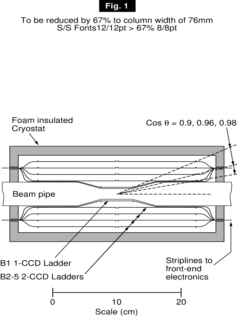
The LC VXD conceptual design is illustrated in Fig. 2. The main goals to be met to achieve this design can be summarised as:
-
•
Utilise large-area CCDs to construct a geometrically elegant, large array.
-
•
Obtain VXD self-tracking with redundancy by building a 5-layer device.
-
•
Require as short a track extrapolation to the IP as possible by putting the first layer as close as 12mm to the beamline.
-
•
Reduce multiple scattering by thinning the ladders to as little as 0.1% per layer.
-
•
Maintain the low occupancy, and hence zero hit confusion, by increasing the pixel readout rate to 50 MHz.
-
•
Improve the radiation tolerance beyond the neutrons/cm2 level.

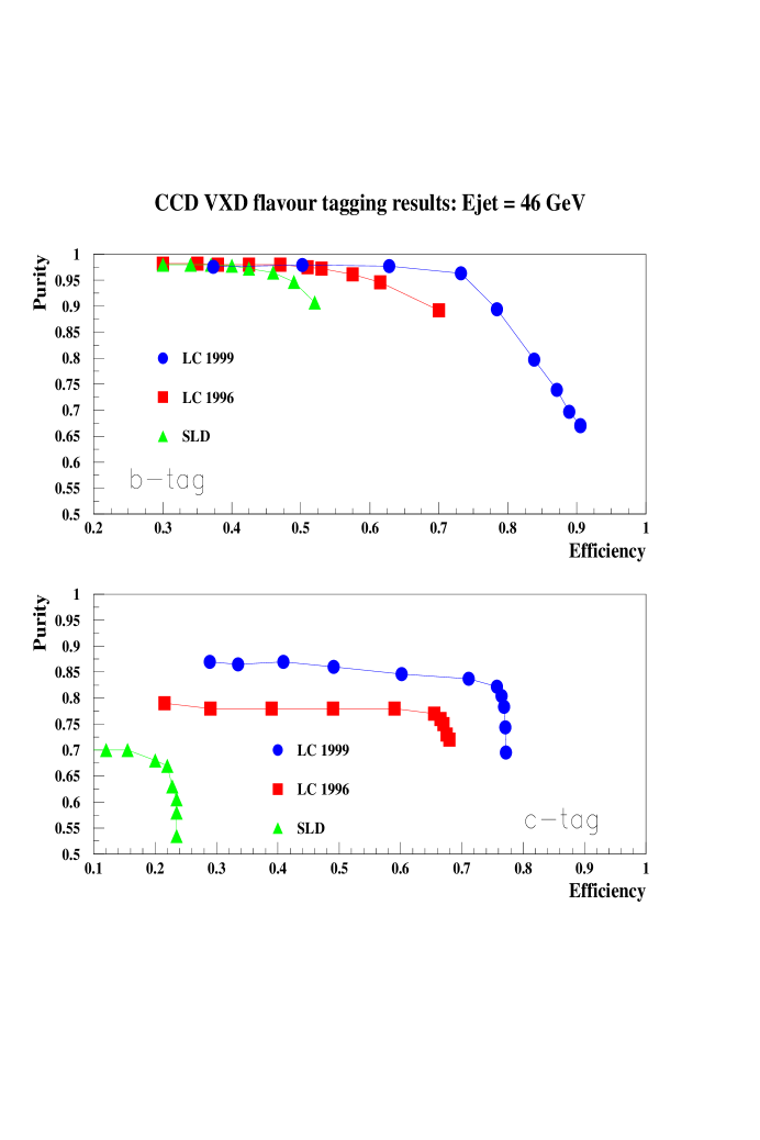
We have simulated the jet flavour-tagging performance that could be achieved with such a ‘dream’ VXD. We have adapted the SLD charm- and bottom-jet tags which are based on the mass of secondary decay vertices [5] reconstructed using a topological vertex-finding algorithm [6]. The purity vs. efficiency trajectories are shown in Fig. 3, where the current SLD results, as well as results for an earlier LC VXD design [7], are shown for reference. For -jet tagging a sample purity of 98% can be maintained for a tagging efficiency up to around 70%, almost a factor of two better than the current (world’s best) SLD VXD3. In the case of -jet tagging a sample purity of 85% can be achieved for an efficiency up to 75%, which is a substantial gain in both purity and efficiency ( 3.5) w.r.t. SLD VXD3.
A substantial R&D programme is needed to achieve this impressive flavour-tagging potential.

5 R&D Programme
The UK-based Linear Collider Flavour Identification collaboration was formed, and was approved by the UK funding committee in October 1998 to initiate a 3-year programme of research and development [8] in order to address these design challenges. The collaboration is working closely with the UK-based CCD manufacturer, EEV, as well as with colleagues in the US and Japan who are also engaged in CCD R&D for the LC VXD.
Table 1 summarises the improvement factors that it is hoped to achieve, relative to the current SLD VXD3, for various parameters.
| Item | SLD | LC | factor |
|---|---|---|---|
| longest CCD (mm) | 80 | 125 | 1.6 |
| largest CCD area (mm2) | 1280 | 3000 | 2.3 |
| ladder thickness (% ) | 0.4 | 0.12 | 3.3 |
| layer 1 radius (mm) | 28 | 12 | 2.3 |
| readout rate (MHz) | 5 | 50 | 10 |
| # ladders | 48 | 64 | 1.3 |
| # pixels (M) | 307 | 700 | 2.3 |
In the first phase of the R&D programme so-called ‘setup grade’ CCDs will be purchased from EEV and used to test individual design aspects. These are typically devices with some defect(s) of a mechanical or electrical nature, but which are perfectly adequate for testing unaffected performance aspects. Two modular CCD test setups are being constructed, one located at the Rutherford-Appleton Laboratory (RAL) and the other at Liverpool University. The aim is to use the two test rigs to focus on complementary aspects: readout and electrical tests at RAL, and radiation damage studies and low-temperature operation at Liverpool. In addition, a metrology setup for mechanical testing and measurement is being developed at Oxford and RAL, which will focus on thin prototype ladder supports and thermal distortion characterisation.
In a later phase custom-made CCDs may be commissioned from the manufacturer, and system design/integration issues will be investigated.
By designing modular test setups in which only the local motherboard is CCD-specific it is hoped that CCDs can be readily exchanged with our US and Japanese colleagues, as well as with different CCD manufacturers.
5.1 CCD Area
A modest increase in length of the longest CCD, by a factor of 1.6, is needed for the geometry shown in Fig. 2, with a corresponding area increase by just over a factor of two. With the widespread movement to 8-, and even 12-, inch wafers in the silicon chip industry there is not believed to be any fundamental obstacle towards manufacturing CCDs of this size. However, the increased area does impinge directly on the rigidity/stability requirements for the low-mass support structures.
5.2 Ladder Thickness
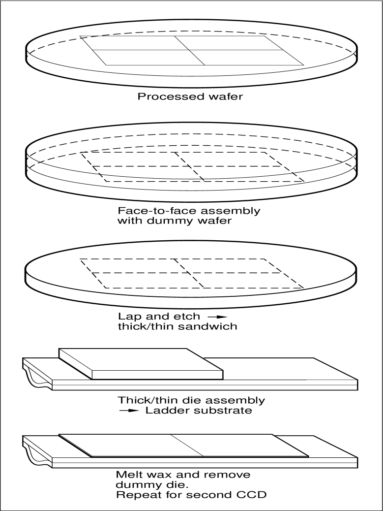
If the CCDs can be successfully thinned down to the thickness of the epitaxial active silicon surface layer, they could in principle be as thin as 20 m, or 0.02% . Such CCDs would, if unsupported, immediately curl up into a ‘swiss roll’, and so the thinning process, and adhesion to a thin (beryllium) support beam, must be carefully thought out.
A schematic thinning process has been devised and is illustrated in Fig. 4. Before thinning one would adhere the top surface of a processed CCD wafer with temporary adhesive, eg.wax, to a dummy wafer. One would then lap and etch the back of the processed wafer to the desired thickness, and dice the wafer into individual CCD units. One would then adhere the back CCD surface to the support beam with permanent adhesive, and finally disengage the dummy silicon block by removing the temporary adhesive.

The support beam itself requires careful design to achieve a low-mass structure with the desired planarity and mechanical stability. One possibility is to use a thin flat Be beam with an intrinsic ‘omega’ or ‘V’ support structure. Finite-element analysis simulations have shown that such structures offer the possibility of small, and predictable, deformations under temperature cycling of the order of tens of m.
If the support beam comprises 250 m Be-equivalent, or 0.07% , and the adhesive an additional 0.02% , the total ladder material budget might be made as low as 0.11% .
5.3 Backgrounds, Inner Radius and Readout Rate
The radial position of the innermost layer w.r.t. the beamline is strongly influenced by the accelerator-related backgrounds, and is correlated with the pixel readout rate, which determines the hit density accumulated during the CCD readout cycle, and hence the degree of fake hit confusion for bonafidetracks.
The main sources of accelerator-related backgrounds are
-
•
Muons from beam interactions with upstream collimators.
-
•
e+e-pairs from converted photons and ‘beamstrahlung’.
-
•
Photoproduced neutrons from the interaction region material and back-shine from the beam dumps.
-
•
Hadrons from beam-gas and interactions.
From the occupancy point-of-view the most serious are the e+e-pairs. For example, beam-beam interaction simulations [9] indicate that tens of thousands of e+e-pairs will be created per bunch crossing of the accelerator. A significant fraction of these populate the 1 GeV tail of the energy distribution, and it is clear that a large detector magnetic field will be required to contain the bulk within the beampipe, and maintain an acceptably low hit density in the VXD. Field strengths of between 3 and 6 T are being considered by the detector working groups. For example, in a 3 T field at TESLA 0.2 hits/mm2 per beam-crossing are expected at the nominal first-layer radius of 12 mm. At NLC/JLC the corresponding figure is 0.1 hits/mm2 in a 6 T field.
At first sight these numbers do not appear forbidding. However, one must then consider the serial pixel readout of the CCD and the time-structure of the accelerator bunch trains. In the NLC/JLC case there are 100 bunches per train, with a bunch separation of 1.4 ns and a train separation of 8.3 ms. Hence if the CCD pixel readout rate is 5 MHz, as in SLD VXD3, it would take roughly 20 bunch-trains to read out a complete CCD, implying an integrated hit density of 200/mm2. Since there are 2500 pixels/mm2 this implies an occupancy of almost 10%, which would lead to significant hit confusion. An occupancy of 1% would be much more manageable, and this could be achieved by increasing the pixel readout rate by a factor of 10, to 50 MHz. This will be one of the main topics in the CCD R&D programme.
In the TESLA design the situation is made more difficult by the fact that there are roughly 3000 bunches per train, with a bunch separation of 337 ns and a train separation of 200 ms. Although a CCD could be read out completely, even at 5 MHz, between bunch trains, the hit density integrated during the readout cycle would be 600/mm2. Even with an increased pixel readout rate of 50 MHz the resulting 60 hits/mm2 is not comfortable. For this reason we are also investigating the possibility of a higher-multiplex CCD readout scheme in which groups of, or even individual, columns would be read out through individual readout nodes.
The hit densities are predicted to be significantly lower at larger radius, and are not expected to be a concern for layers 2-5, which lie at 24 mm from the beamline. If the inner layer were omitted, or if the whole detector were pushed out in radius to start at 24 mm, the extrapolation from the first track hit back towards the IP would be doubled, and our simulations have shown that the flavour tagging performance would be noticeably worse. Moreover, the backgrounds in the real accelerator may be larger than the current estimates suggest, so that in any case an increased CCD readout rate will help to secure additional ‘headroom’ against such an eventuality.
It is likely that by a combination of increased pixel readout rate and multiplexed CCD readout, a large detector B-field, and in the last resort a (compromised) larger inner layer radius, the hit density can be kept at or below the 10 hits/mm2 level.
5.4 Radiation Damage Studies
Preliminary simulations [9] have indicated that the neutron flux in the inner detector may be at the level of - 109 per cm2. Though orders of magnitude less than at the LHC, the rate is large enough that more detailed simulations are warranted, and that consideration be given to the radiation tolerance of the CCDs.
In many years of normal operating conditions at SLC, no radiation damage was observed in the CCDs. However, during one unusual period in which undamped beams were delivered for accelerator studies a noticeable charge-transfer inefficiency (CTI) was observed. This effect was completely ameliorated by cooling the CCDs by an additional 20 degrees to around 185 K.
Neutrons are believed to cause a CTI by producing bulk damage sites in the silicon lattice, which act as charge-trapping centres. The minimum-ionising signal of roughly 2,000 electrons typically undergoes several thousand serial transfers from pixel to pixel before reaching the readout node, and a CTI of would cause a serious loss of signal. In recent neutron irradiation studies [10] using VXD3 CCDs, corresponding to an integrated dose of 6.5 1-4 MeV neutrons/cm2, a mean m.i.p. signal loss of 29% was observed. Interestingly, after flushing the CCD with charge, the loss was reduced to 18%, and reduced further to 11% by lowering the operating temperature from 185 K to 178 K.
These studies suggest that charge-flushing may serve to fill, at least temporarily, the charge traps caused by radiation damage, and that the full-trap lifetime can be extended by lowering the temperature. We intend to pursue both approaches and there is good reason to believe that CCDs can be made radiation tolerant at the 1010 neutrons/cm2 level, which is 1-2 orders of magnitude above the estimated flux at the LC. In addition, the development of more optimised shielding strategies may serve to reduce the expected neutron flux in the interaction region. Finally, ideas to reengineer the CCD architecture, so as to reduce the effective charge-storage volume and hence the sensitivity to bulk damage, may also be pursued.
6 Summary and Outlook
In summary, CCDs offer a very attractive option for a high-energy linear collider vertex detector. CCD VXDs have been ‘combat-tested’ at the first linear collider, SLC, and have allowed SLD to achieve unrivalled and -jet tagging performance. Through further improvements, via the production of thinner, larger-area, faster-readout CCDs, there is every reason to expect that 21st-Century flavour-tagging at the next-generation linear collider will be substantially better, and able to meet the demands of high-efficiency tagging in a multijet environment.
Groups centred in the USA/Japan and Europe are currently preparing the technical design reports for the accelerator and detector(s), which will be presented to the respective funding agencies in 2001/2. From the technical point-of-view construction could start as early as 2003, with first physics in 2008/9.
The LCFI Collaboration has started an R&D programme to address the CCD design issues, such that a vertex detector blueprint could be credibly produced on a matching timescale. We look forward to presenting the first results of this endeavour at Vertex2000!
References
-
[1]
C.J.S. Damerell et al., IEEE Trans. Nucl. Sci. 33 (1986) 51.
S. Barlag et al., Phys. Lett. B184 (1987) 283. - [2] T. Abe, these proceedings.
- [3] C.J.S. Damerell et al., Nucl. Instr. Meth. A288 (1990) 236.
- [4] K. Abe et al., Nucl. Instr. Meth. A400 (1997) 287.
- [5] See eg., SLD Collab., K. Abe et al., Phys. Rev. D59 052001 (1999).
- [6] D.J. Jackson, Nucl. Instr. Meth. A388 (1997) 247.
- [7] C.J.S. Damerell, D.J. Jackson, Proceedings of Snowmass 96 Workshop, p. 442.
-
[8]
LCFI (UK) Collaboration, ‘A proposal to initiate Research and Development for
a Vertex Detector at the future e+e-collider’, S.F. Biagi et al.:
http://hep.ph.liv.ac.uk/~green/lcfi/lcfihome.html. -
[9]
O. Napoly, talk at LCWS99, Sitges, Spain:
http://www.cern.ch/Physics/LCWS99/talks.html. -
[10]
N. Sinev, talk at LCWS99, Sitges, Spain:
http://www.cern.ch/Physics/LCWS99/talks.html