Design and Tests of the Silicon Sensors
for the ZEUS Micro Vertex Detector
Abstract
To fully exploit the HERA-II upgrade, the ZEUS experiment has installed a Micro Vertex Detector (MVD) using -type, single-sided, silicon -strip sensors with capacitive charge division. The sensors have a readout pitch of 120 m, with five intermediate strips (20 m strip pitch). The designs of the silicon sensors and of the test structures used to verify the technological parameters, are presented. Results on the electrical measurements are discussed. A total of 1123 sensors with three different geometries have been produced by Hamamatsu Photonics K.K. Irradiation tests with reactor neutrons and 60Co photons have been performed for a small sample of sensors. The results on neutron irradiation (with a fluence of 1 MeV equivalent neutrons / cm2) are well described by empirical formulae for bulk damage. The 60Co photons (with doses up to 2.9 kGy) show the presence of generation currents in the SiO2-Si interface, a large shift of the flatband voltage and a decrease of the hole mobility.
DESY–02–215
Introduction
The HERA collider underwent a major upgrade [1] during the years 2000-2001. The aims are to increase the maximum luminosity from 1.5 to cm-2 s-1 and to provide longitudinally polarized electrons for the collider experiments H1 and ZEUS, thus giving higher sensitivity to electro-weak physics and physics beyond the Standard Model. The ZEUS experiment [2] has been equipped with new forward tracking detectors (in the proton beam direction), the Straw Tube Tracker (STT) and the Micro Vertex Detector (MVD). They improve the precision of the existing tracking system, and allow the identification of events with secondary vertices produced by the decay of long-lived states like hadrons with charm or bottom quarks and leptons. The detector acceptance will be enhanced in the forward region, along the proton beam direction, improving the detection of scattered electrons in neutral current deep inelastic events with very high squared momentum transfer, . Moreover, it will help in the reconstruction of the interaction vertex in charged current deep inelastic events at high values of the Bjorken scaling variables, [3]. The MVD is composed of a barrel (BMVD) and forward (FMVD) part. The MVD has to fit inside a cylinder of 324 mm diameter defined by the inner wall of the Central Tracking Detector (CTD). The readout electronics, based on the HELIX 128-v3.0 [4] chip has been mounted inside the active area, nearby the silicon sensors. For the construction of the BMVD and FMVD subdetectors 600 and 112 sensors, respectively, were needed; more details on the MVD design and mechanical structure can be found in [5].
After an introduction to the silicon sensor and the test structures designs, the paper covers the tests performed to verify the technological parameters [6, 7]: bulk capacitance and depletion voltage, coupling and interstrip capacitance, leakage current stability, biasing, aluminum and strip resistances, field capacitor, pmos transistor and gate controlled diode measurements. After a brief description of the radiation environment at HERA, based on the experience of the 1992-2000 running period, the irradiation tests are presented: neutron irradiation, with fluences of 1 MeV equivalent neutrons/cm2 and 60Co photons with doses from 50 Gy up to 2.9 kGy. A description of the sensor parameters affected by hadronic and electromagnetic radiation is given in the last section of the paper, before summarizing the results of the electrical tests.
1 Silicon sensor design
| sensor type | n-type Si, single sided implants |
| resistivity | kcm |
| full depletion voltage | V |
| active volume thickness | m |
| readout | Al readout strips on strips, AC coupled ( - double layer) |
| readout strip pitch | m |
| readout strip width | m |
|
number of interstrips
between two readout strips |
5 |
| interstrip width | m |
| Al readout strip width | m |
| backplane | thick layer, aluminized |
| strip biasing | poly-Si resistors |
| number of guard rings | 3 |
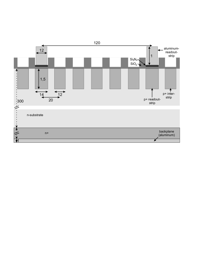
The specifications for the silicon sensors, produced by Hamamatsu Photonics K.K. [8], are summarized in Table 1; the sensors are made of high resistivity -type silicon ( kcm), m active thickness. One side of the sensors is covered by 12 m wide doped strips with a pitch of 20 m; the backplane of the sensor has a thick layer and is aluminized. The readout strip pitch is 120 m: every sixth strip is 14 m wide, and AC coupled to a m wide aluminum readout strip. The coupling capacitance of the readout strips is achieved with a double layer of and . A schematic cross section of the sensor is shown in figure 1.
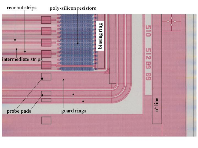
The biasing of the strips is implemented using poly-Si resistors. As can be seen from figure 2, every second strip is connected to the ground line (called the biasing ring) on one side, the remaining strips are connected on the opposite side (not shown in the figure). The first and last readout strips complete the ring being directly connected to the biasing ring. Three guard rings surround the biasing ring; beyond the last guard ring, at the sensor edges, an line is placed to enable reverse biasing of the sensor directly from the top. The guard rings surround the active area. The innermost guard ring carries the currents generated from defects outside the sensor’s sensitive volume. During detector operation, the two outmost guard rings will be left floating, while the inner guard ring will be connected to ground via a resistor, protecting the sensor active area even in the case of high generation currents from the edge.
Three different sensor geometries have been defined: square sensors for the BMVD, and two wedge shaped sensors for the FMVD. A picture of one corner of the BMVD sensor layout is shown in figure 2.
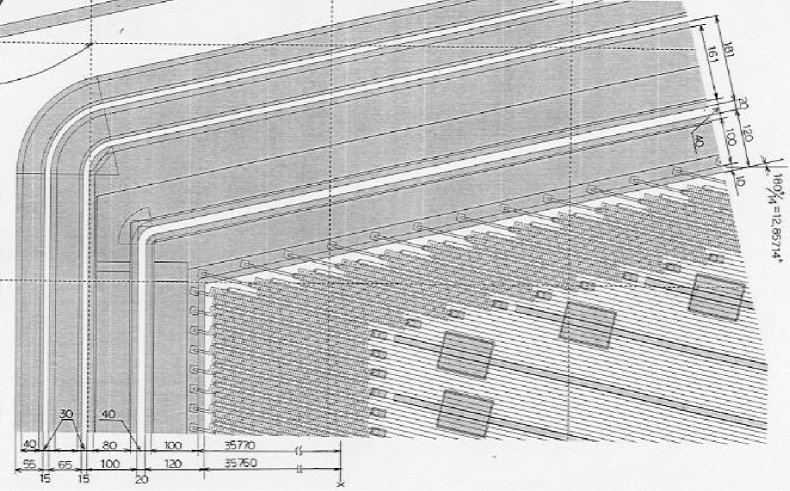
The layout for the FMVD sensors is shown in figure 3.
| type | shape | dimensions | strip length | # of readout strips | active area |
|---|---|---|---|---|---|
| BMVD |
![[Uncaptioned image]](/html/hep-ex/0212026/assets/x4.png)
|
h=64.2 mm
w=64.2 mm |
62.2 mm | 512 | 38.6 cm2 |
| FMVD1 |
![[Uncaptioned image]](/html/hep-ex/0212026/assets/x5.png)
|
h=73.5 mm
w1=64.3 mm w2=30.7 mm |
5.6 - 73.3 mm | 480 | 32.6 cm2 |
| FMVD2 |
![[Uncaptioned image]](/html/hep-ex/0212026/assets/x6.png)
|
h=48.5 mm
w1=64.1 mm w2=42.0 mm |
5.6 - 47.7 mm | 480 | 23.9 cm2 |
Table 2 contains the relevant geometrical parameters of the three different silicon sensors. The FMVD sensors have a trapezoidal shape with the tilted edges inclined by with respect to the height. The strips run parallel to one tilted side and have a varying strip length: from 5.6 mm for the 1st strip to 73.3 mm (for strip number 254) for the FMVD-1 and 47.7 mm (for strip number 153) for the FMVD-2. The active areas of the three sensor types correspond to 93% of the mechanical area. A probe pad, with an area of m2 is located close to each poly-Si resistor (see figure 2 and 3). The BMVD sensors have three rows of bond pads, with a pad area of m2, located at 8, 10 and 19 mm from one sensor edge. The FMVD sensors have only one row of bond pads perpendicular to the readout strips and therefore to one of the tilted edges of the sensor.
Capacitive charge division between the readout strips is used in order to limit the number of readout channels. By means of capacitive coupling between strips, the charge collected at intermediate strips induces charges on the readout strips which are approximately inversely proportional to the distance between interpolation and readout strips [9]. Uniformity in charge collection is achieved by keeping all the strips (readout and intermediate) at the same potential.
2 Test structures design
Since not all the specifications and technological parameters can be directly measured on the sensors, special test structures have been designed and produced on the same wafers as the sensors. With the help of the test structures it is also possible to repeat measurements after assembly and installation of the detector, when the silicon sensors are no longer accessible for most of the electrical measurements. Moreover, measurements that might damage a sensor can be performed on the test structures.
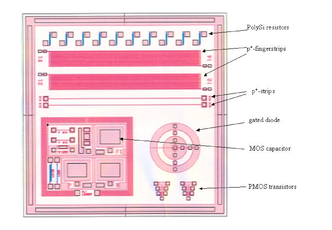
A picture of the test structures layout is shown in figure 4.
The following structures are implemented and used for measurements:
-
•
poly-Si resistors. 10 poly-Si resistors on each test field allow direct measurement of the value of the biasing resistors.
-
•
finger-strips. Each of the two finger-strip structures consists of two neighboring strips in a fork-like shape with a total strip length of 53.5 mm. The strips are covered by aluminum strips of m width. The two different finger-strip structures have a strip width of m (W12) and m (W14). The strip pitch is m and the gap between the strips is m (W12) and m (W14). The and aluminum strips are accessible with contacts on both sides. The structure has been used to measure the capacitance and the resistance between neighboring strips, which cannot be contacted on the sensor. The geometry of the finger-strips is similar to the strips on the sensor, apart from the width of the aluminum strips (m instead of m) and the presence of interstrips on the detectors, which are not covered by aluminum strips.
-
•
strips. Two separated strips with m (W12) and m (W14) strip width and a length of m each, allow measurement of the resistivity of the implant for readout (W14) and intermediate (W12) strips.
-
•
Gated diode. The gate controlled diode is a standard component for the investigation of surface effects on junctions [10]. For the MVD test structures a design with two gates and one guard ring has been chosen. In this work it has been used to investigate the surface generation current before and after 60Co irradiation. Also the flatband voltage has been determined from the gated diode measurements.
-
•
MOS capacitor. With the MOS capacitor the characteristics of the surface region can be investigated [10]. Besides the measurement of the oxide thickness it has been used to determine the flatband voltage from which the amount of positive oxide and interface charges has been calculated.
-
•
PMOS transistor. The PMOS transistor is a surface field-effect transistor. PMOS transistors with three different width/length ratios have been used to extract the threshold voltage, which is related to the flatband voltage, and to determine the mobility of holes in the interface area below the gate oxide. Also the gated diode has been used as a PMOS transistor.
-
•
Pad diode. In addition to the structures shown in figure 4, a pad diode consisting of a pad (3.6 mm 3.6 mm) on top of the silicon bulk and three guard rings around the active area was used. It allows the study of the characteristic of the junction with reduced edge effects from the SiO2 region, compared to the situation on the sensor.
3 Electrical measurements
3.1 Test setup
The main electrical parameters have been measured on a probe station.
The stainless steel chuck, where the device under test (DUT) is held
with vacuum during the measurement, is connected to a PT100 temperature sensor
to monitor the temperature during the measurements.
The temperature sensor measures with an accuracy of about
0.5∘C at room temperature.
A combined voltage source and pico-ampere meter Keithley
487 [11] is used to bias the DUT.
The current resolution varies from fA,
for currents in the nA range, to 10 nA for currents in the 2 mA range.
For capacitance/voltage (C/V) and impedance measurements, a Hewlett Packard
4263A LCR meter [12] is used;
possible measurement frequencies are f = 120 Hz, 1 kHz, 10 kHz and 100 kHz.
The resolution is 1 fF at f = 10 kHz.
Another LCR meter, the Hewlett Packard 4192A, was used for investigating
frequency dependencies in detail. It can measure over a continuous
frequency range from 5 Hz to 13 MHz. The resolution is 10 fF
at f=10 kHz.
All the measured currents have been scaled to T = 293 K according to
the equation
which corrects for the temperature dependence of bulk generation currents [13]. is the effective energy gap at T = 293 K, eV, and is the Boltzmann constant. For T = 293 K, the change in current is about 8%/K. For surface generation currents the formula above can be used after replacing with [13]. The difference of the corrections given by the two formulas is negligible in the temperature range of our measurements: K.
3.2 Depletion voltage

The impact of the depletion voltage on the sensor performance can be summarized as follows:
-
•
Sensors operated above full depletion achieve an optimal resolution and charge collection efficiency: high depletion voltages lead to high electric fields in the sensor, decreasing the charge collection time.
-
•
Large electric fields may cause local avalanche breakdown in critical regions (i.e. at the - Si - SiO2 interface), resulting in an increase of the leakage current or unstable behavior.
-
•
A combination of high leakage currents and high depletion voltages increases the power consumption in the sensor. Increase in temperature will raise the current, resulting in additional noise and possibly unstable behavior.
-
•
Hadronic radiation will decrease the depletion voltage until type inversion occurs. Sensors with high depletion voltage will reach type inversion at higher fluences.
Based on the previous arguments, and on the availability of detector-grade silicon, an initial value V, corresponding to kcm, was specified. C/V measurements have been performed on the sensor to extract the depletion voltage: with the first guard ring grounded, the bias voltage was applied between the sensor backplane and the biasing ring. The distribution of the depletion voltages of the sensors, extracted from the C/V characteristics measured for each sensor delivered by the manufacturer, is given in figure 5. Plot (a) shows the values for the BMVD sensors: four groups of sensors are observed, in the region V, corresponding to a resistivity kcm. Plot (b), obtained for the FMVD sensors, reveals similar properties of the material used. All values are within required specifications; the structure reflects the fact that the sensors are delivered in batches.
For 25% of the sensors a C/V measurement was performed after delivery: the agreement on with the manufacturer values is better than 1 V.
The average value for the minimum capacitance pF (1 kHz measurement frequency), is in good agreement with a geometric capacitance pF, where cm2 and m denote the effective area and thickness of the sensor, respectively.
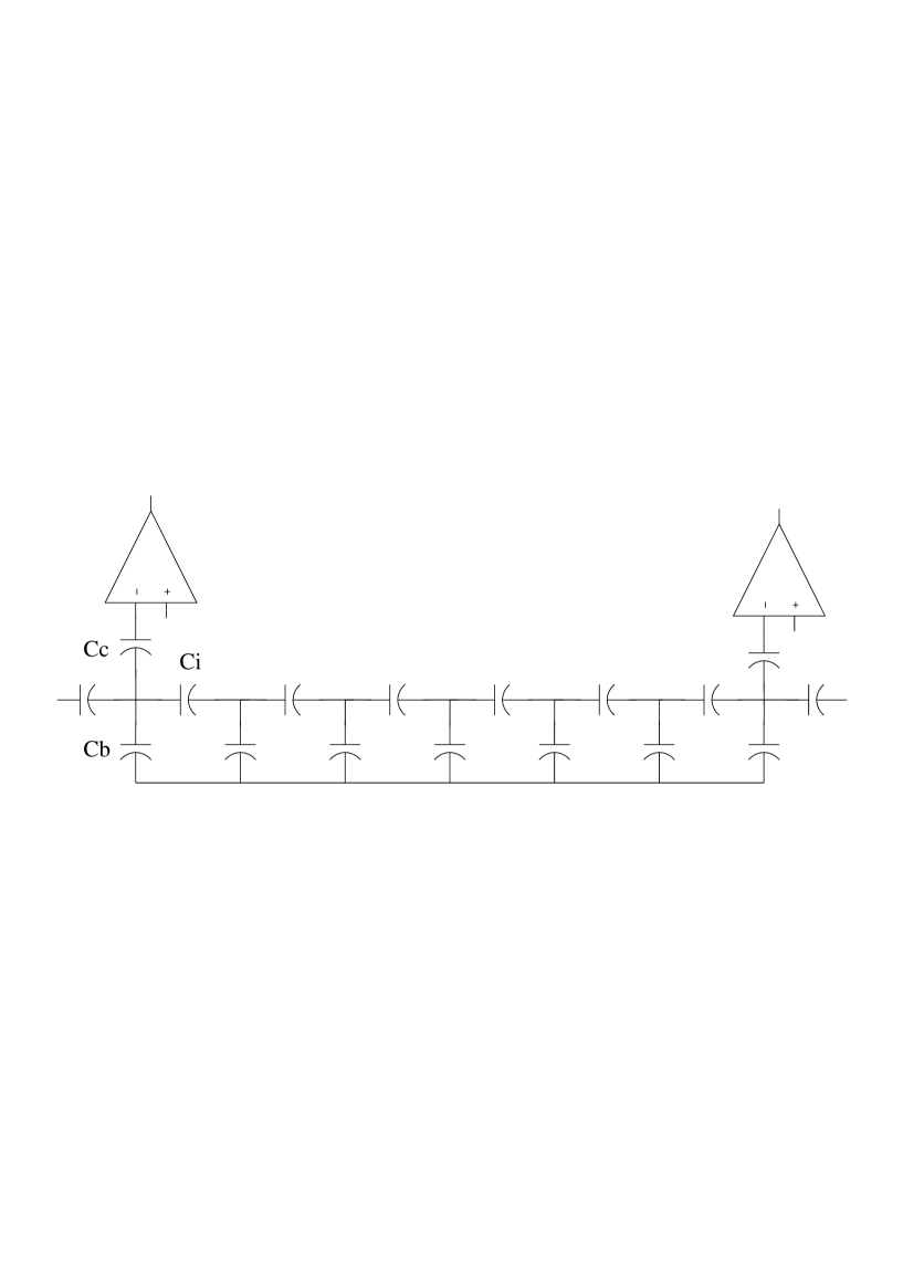
From the total capacitance an estimate of pF/cm for the single strip to backplane capacitance is obtained. Figure 6 shows a simplified scheme of the capacitance network of the sensor.
From the measured spread of 4 pF for , assuming the same active area for all sensors, we conclude that the variation of the effective sensor thickness is less than 1%.
3.3 Interstrip capacitance
The interstrip capacitance was measured on the finger-strip test structures.
 |
 |
|
| (a) | (b) |
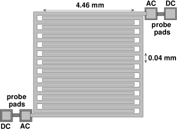
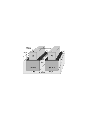
Figure 7 (a) shows a schematic drawing of the fingerstrip: a direct contact to the implant (DC) and a contact to the aluminum strip (AC), on both sides of the structure, allow one to measure the interstrip capacitance between the strips. A 3D view of two neighboring strips is given in figure 7 (b). By measuring the capacitance between all combinations of the four probe pads (AC and DC) it is possible to extract the capacitance between two strips and estimate the effect of the next neighbors and the couplings Al-Al and Al-.
The capacitance measurements have been performed using the HP4263A with a frequency of 10 kHz. The capacitance between neighboring -strips for and wide implants are pF/cm and pF/cm, respectively. The capacitance between a readout strip ( wide) and the next strip () has been estimated as the mean value of and : pF/cm.
The capacitance between aluminum strips, , on the finger-strips and the capacitance between neighboring aluminum and strips, , are: pF/cm, pF/cm and pF/cm, pF/cm, in very good agreement with a SPICE simulation [7].
3.4 Coupling capacitance and quality of coupling oxide
The readout strips are AC coupled to the input channels of the front-end electronics preamplifiers. The HELIX-128 input capacitance is a sum of the sensors coupling capacitance, , and the effective input capacitance of the preamplifier, . The input capacitance has to be large compared to the sensor interstrip and backplane capacitances. This minimizes the signal loss to the sensor backplane and to the neighboring channels which would deteriorate the resolution and the charge collection efficiency. The coupling capacitance is formed by a double layer of SiO2 and Si3N4 between the and the Al strips; its value depends on the area of the - and readout-strips and the thickness of the double layer. has been specified pF/cm, which is sufficiently large compared to the backplane capacitance, pF/cm and the interstrip capacitances pF/cm. Measurements of , in series with the biasing resistor, have been performed directly on the sensors; a direct measurement between the Al strip and the implant has been done on the single strips on the test-structures. Typical measured values, pF/cm, are within the specification.
The manufacturer provided, for each batch of sensors and test structures, a measurement of the coupling capacitance (measured at 10 kHz). These values vary between pF/cm and pF/cm for the complete production period (1123 sensors).

Figure 8 shows a measurement of the coupling capacitance for an FMVD1 sensor as a function of the strip length. The pad capacitance , which contributes as an offset to the measured capacitance, can be extracted as the intercept of the data fitted with a line. The estimated value is pF [7], while from geometrical considerations the expected pad capacitance is pF. The slope of the fit gives the measured coupling capacitance, pF/cm.
Pinholes in the SiO2 layer can introduce a DC connection between the implant and the aluminum readout strip: the sensor leakage current will flow directly into the charge amplifier and may saturate it. The double layer technology has been chosen to combine the advantages of both isolation materials: large resistivity for the SiO2 and the negligible number of expected pinholes in the Si3N4. The quality of the coupling layer has been specified with the maximal leakage current through the coupling capacitor pA at V, where is the voltage difference between implant and readout strips. Measurements of and of the breakdown voltage, , have been performed directly on the sensor, applying a voltage between the biasing line and single readout strips. For all measured prototype sensors the specifications were fulfilled with pA at V.

The plot of figure 9 shows an example of a destructive measurement: the breakdown voltage is found to be around 120 V, while is well below the specified value of 20 pA up to .
3.5 Total leakage current
The sensor leakage current through the strips affects the sensor performance mainly as a source of noise for the preamplifier input. For a CR-RC pulse-form shaper, used in the HELIX-128 [4] readout chip, the noise level in terms of the Equivalent Noise Charge (ENC) increases with the square-root of the leakage current: , where is the single strip leakage current, is the peaking time of the signal shaper ( ns for the HELIX chip) and is the elementary charge. Due to the large number of readout strips, a high value of the sensor leakage current of for instance , uniformly distributed over the sensor volume, yields a noise contribution , which is a small fraction of the signal of a Minimum Ionizing Particle (MIP) of .
The limiting factor for the leakage current is the chosen biasing scheme with protection resistors, which will reduce the voltage on the sensors in case of high currents.
For the sensor specifications a maximum value of the leakage current A at a bias voltage V has been chosen. The manufacturer has provided, for each sensor, two current/voltage (I/V) characteristics (from 0 to 200 V), measuring:
-
•
the sensor leakage current flowing through the biasing ring, with first guard ring grounded;
-
•
the first guard ring current, with biasing ring grounded.

A distribution of the leakage currents at V, is shown in figure 10 for the BMVD and FMVD sensor, respectively. The currents, which have been normalized to the active area for direct comparison, are small, nA/cm2.

Two examples of I/V characteristics are shown in figure 11 for the biasing and first guard ring currents, respectively. The two curves correspond to sensors with the same depletion voltages, V. The biasing ring characteristics (figure 11 (a)) shows that the leakage current reaches between 60% and 90% of the maximum value already within the first 3 V; afterwards the current continues to increase slightly even after is reached. This behavior shows a significant contribution from generation currents at the Si-SiO2 interface; as soon as this interface becomes part of the depleted volume it contributes to the sensor leakage current. The bulk generation currents, which have a behavior proportional to , show a small (full dots curve) or even negligible contribution (open dots curve) to the total leakage current of figure 11 (a). The guard ring current is shown in figure 11 (b); it is typically about 6% and always below 10% of the total leakage current. The guard ring structure becomes very important in the case of type inversion, when the depletion layer starts growing from the sensor backside, leading to a larger lateral extension of the depletion zone [14].
The total leakage current has to be limited and stable during the long-term operation in the ZEUS environment, in order to ensure a proper functioning of the sensor system with respect to the cooling system and the design of the power supplies. High and unstable leakage currents can also indicate problems of the manufacturing technology.

Therefore a long term test of the sensor currents has been performed for all
sensors. The sensors were biased at 200 V and the current
flowing through the biasing ring (with all the guard rings floating)
was measured for a period of at least 24 hours.
A scatter plot of the start () and end currents ()
is shown in figure 12 for the BMVD sensors:
the great majority of the sensors show a stable behavior;
only for 2 out of the 748 tested sensors
a fast increase of the current is seen with an end value of several A
above the specified value of 2A.
Similar results have been obtained for the FMVD sensors.
3.6 Biasing resistance
Each strip on the sensor is connected to the biasing ring through a poly-Si resistor. The purpose of these resistors is to keep all the strips at the same potential without losing signal charge to the biasing ring. The biasing resistors are sources for parallel thermal noise at the preamplifier inputs of the readout channels. A high value for the biasing resistors is thus desirable for a small noise in the readout channels. Large differences in the resistance values between neighboring strips could (for large dark currents) result in a spread of the strip potentials. This would cause a distortion of the electric field below the strips and distort the position measurement. The specified range for the poly-Si resistors is M. Since on the sensor the poly-Si resistors are not accessible with a direct DC contact, 10 poly-Si resistors have been produced on each test-structure with probing-contacts on both sides.
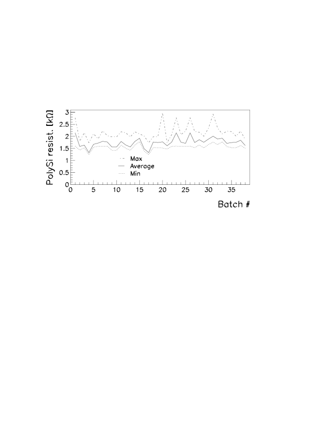
Figure 13 shows the value of the poly-Si resistor as a function of the production time, as provided by the manufacturer. The average measured values vary between 1.3 M and 2.2 M, which is slightly above the specified value, but does not influence the sensor performances [6].
For a sample of sensors, the values of the poly-Si resistors have been measured after delivery. The spread of the resistance values within one wafer was always found below M.
3.7 strip resistance
A small resistance of the implants reduces the charge-spread time constant of the strips. The number of acceptors in the implant has to be several orders of magnitude larger than the number of donors in the depletion region of the sensor; only then do all field lines end in strips. This will be achieved for standard implantation depths if the resistance is of the order of the specification value of kcm. The implant width of the readout- strips is m (W14) while the width of the intermediate strips is m (W12). Since the resistance of a single strip cannot be measured directly on the sensors, all measurements have been performed on the test-structures through an I/V-measurement, applying a DC-voltage between both sides of the strip and measuring the current flowing through the strip.
For the W14 strips a resistance kcm has been measured. For the W12-strips the values were kcm.
Assuming a depth of the implants of about m [15], the doping concentration of the implants can be derived from the resistance:
where the resistivity cm, with the cross section perpendicular to the W12 implant length. For the hole mobility a value cm(V s) for high doping concentration has been used [10].
3.8 Interstrip resistance
The ohmic resistance between two neighboring strips affects the charge division performance of the sensor. Charges in the SiO2, interface charges and electron accumulation layers below the oxide may affect the potential between the strips inducing a change in the interstrip resistance.
The measurement of the - I/V characteristic has been performed on the fingerstrip test structure connecting one DC contact to the voltage generator and measuring the current flowing through the other DC contact. The backplane of the structure is connected to an additional power supply.
A set of I/V curves for different backplane voltages is shown in figure 14 for the W12 structure.
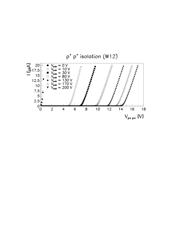
Two regions can be distinguished:
-
•
below a threshold voltage, , the interstrip resistance is very high, G cm;
-
•
after is reached, the slope of the I/V curve changes to values of about M cm.
The threshold voltage at which charge injection leads to a current between the strips, increases with increasing backplane voltage: from V at V to V at V. The interstrip resistance for the W14 structure is G cm.
For a sensor with , a low resistance k cm is observed around V.
3.9 Aluminum strip resistance
The readout strips are covered with a double layer of SiO2 and Si3N4 and an aluminum layer on top, which allows direct connection to the HELIX-128 preamplifier. Thanks to kcm for the strips resistance, the charge collected during the integration time of the HELIX chip, will not spread along the strip but remain where the charge is collected at the strip. A large value for the aluminum strip resistance, , would form a low-pass-filter with the coupling capacitance (double layer of SiO2 and Si3N4), for particles crossing the sensor far away from the connection to the readout electronics. The result would be a loss of signal height depending on the position of the particle along the strip. For the MVD sensors cm has been specified. Measurements performed on the test structure result in values lower than cm, which are consistent with those provided by the manufacturer.
3.10 MOS capacitor measurements
Measurements on a MOS capacitor are used to extract the information on the oxide region and the surface between the strips. A typical C/V characteristic of the MOS capacitor is given in figure 15, with the voltage applied between the aluminum gate and the backplane.

In the accumulation region, for V, the positive charges in the oxide and at the Si - SiO2 interface are compensated by electrons accumulating in the bulk close to the interface. Since the doped bulk is not depleted, the measured capacitance corresponds to the capacitance of the oxide, from which the field oxide thickness m (with pF and cm2) can be extracted. As the voltage decreases, the depletion region is reached, where electrons are repelled in the bulk from a negatively biased gate. A positively charged zone depleted of free carriers is created below the oxide. Acting as an insulator the capacitance decreases. The flatband voltage, , is reached when the charges in the oxide and the difference of the work function between aluminum and silicon () are compensated. A more negative voltage will build up holes below the SiO2 forming an inversion layer. The measured capacitance corresponds to the series of the oxide and depleted bulk capacitance .
From the flatband voltage the density of oxide and interface charges can be extracted: . The flatband voltage is determined as the voltage where the maximum slope of the C/V curve is observed (for a compilation of different ways to extract the flatband voltage see [16]). A measured value of V (see figure 15) corresponds to charge states/cm2.
3.11 Hole mobility in the interface area
The PMOS surface field effect transistors have been used to measure the hole mobility and to study the effect of irradiation: a decrease of the hole mobility indicates additional defects at the SiO2 - Si interface. The gate controlled diode has been used as a PMOS transistor. A circular geometry is preferable due to reduced edge effects compared to linear geometries for narrow channels, when the drain and source depletion zones extend into the gate area, with the effect of lowering the threshold voltage.

Figure 16 shows an I/V characteristic for the gate controlled diode used as a PMOS transistor with width over length, W/L=5.7. For small drain voltages , the transistor operates in the linear region where the drain-source current is well approximated by [10]; is the gate voltage. The threshold voltage is reached when the gate voltage has compensated the positive charges in the oxide and the work function difference and starts building an inversion layer. From the previous formula, the gate voltage reaches the threshold voltage when the extrapolated I/V curve, from the linear region, intersect the line. A threshold voltage V has been measured for non-irradiated test structures. Similar values have been measured on the PMOS FET structures.
The slope of the I/V curve is proportional to the hole mobility, . Assuming an oxide thickness m, as derived from the MOS capacitor measurements, the mobility of the holes below the gate, cm2/(V s) has been estimated. Similar values between 220 and 240 cm2/(V s) have been measured using the linear PMOS transistors.
3.12 Gate controlled diode measurements
The gate controlled diode structure allows a direct measurement of surface and bulk generation current contributions to the total leakage current. A detailed description of the gate controlled diode structure can be found in [10].
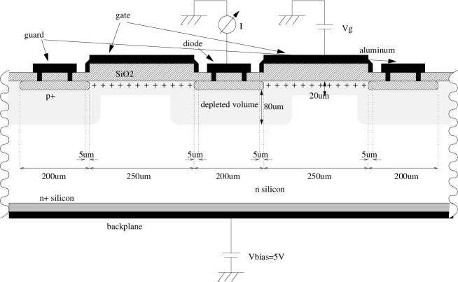
A cross section of the gate controlled diode on the test structures is shown in figure 17 with the connection scheme used for the measurements. The expected depletion volume is also sketched. The diode leakage current, under reverse bias, is measured as a function of the gate voltage applied to the aluminum gate.

Figure 18 shows a typical I/V characteristic for a
non-irradiated structure with a bias voltage V.
Accumulation, depletion and inversion regions can be distinguished clearly:
the accumulation plateau is at V, the depletion zone
is in the range V and finally the inversion
plateau is at V.
In the following we focus on the estimate of the surface generation
current, , which is given by the current difference of the depletion and
inversion plateau. A value pA can be read from
figure 18, which corresponds to 2 nA/cm2.
The surface recombination velocity is obtained from
as , where is the elementary charge,
is the area of the gate electrode and is the intrinsic charge
carrier density in silicon. A value of cm/s is obtained.
4 Irradiation tests
The main sources of background radiation at HERA are electrons or positrons from lepton-beam-loss-accidents and direct- and back-scattered synchrotron radiation. In addition, contributions from charged and neutral hadrons due to unstable beam conditions are expected. During the years of HERA-I operation (1992-2000) the experiments accumulated an average dose of 50 Gy/year [17].
To increase the instantaneous luminosity for the HERA-II runs, the separation of the two beams has been shifted closer to the interaction region. Two superconducting magnets have been installed inside the detector, at few meters from the interaction points to do this. Nevertheless the expected integrated dose should not change considerably. The beam currents will not change appreciably and the possible backscattered photons and electrons from synchrotron radiations should be shielded by means of collimators located inside the beam pipe111Experience from the first running period of HERA II showed higher levels of backscattered synchrotron radiations. The bigger part of the radiation collected came from beam losses in the ZEUS interaction region.
Radiation studies on the silicon sensors have been performed assuming a maximum dose of 3 kGy, which should be well above the expected integrated dose. Two different sources have been used for the studies:
-
•
reactor neutrons with energies peaked at 1 MeV and ranging from thermal energies up to 10 MeV.
-
•
low energy photons ( MeV) from a 60Co source;
4.1 Results on neutron irradiation
The irradiation was performed at the TRIGA MARK II Research Reactor in Ljubljana, Slovenia. The sensor and the corresponding test structure were irradiated without bias in a single irradiation step with a fluence 1 MeV neutrons /cm-2.
4.1.1 Depletion voltage and capacitances

Hadronic irradiation, in particular low energy and thermal neutrons cause displacement damage in the silicon lattice of the bulk, resulting in a change of the effective doping concentration . This mechanism leads to a decrease in the depletion voltage until type inversion occurs. The bulk damage leads to a fluence-proportional increase of the bulk generation current (cf. [18] for studies on the effect of hadronic irradiation on silicon sensor properties).
The effect of hadronic radiation on the depletion voltage was studied measuring the C/V characteristics before and after irradiation.
The depletion voltage of the sensor was V before irradiation. One day after irradiation it was V, after 17 days it had increased to V (see figure 19).
According to the Hamburg model [19, 18] for hadronic radiation damage and annealing, the change in the effective doping concentration can be expressed as function of time and of the fluence as
where represents the stable damage, the short term annealing and the reverse annealing component.
All parameters are taken at room temperature. The model predicts, for a sensor irradiated with a fluences 1 MeV equivalent n/cm2 and our initial parameters, a depletion voltage V after one day and V after 17 days, in good agreement with the measured values.

No change in the interstrip capacitance has been observed, as shown in figure 20.
4.1.2 Leakage current
An increase of the leakage current was observed; a total current of A at 100 V was measured one day after the irradiation with a fluence 1 MeV equivalent neutrons/cm2. After 17 days of annealing at room temperature the measured current was A, at the same bias voltage. Using the parametrization described in [18], the predicted values of leakage currents are A and A after 1 day and 17 days of annealing time at room temperature, respectively.

The I/V characteristics for the neutron irradiated sensor is shown in figure 21 before and after irradiation.
4.2 Results on 60Co irradiation
Low energetic irradiation mainly causes damage in the SiO2 at the Si-SiO2 interface. The damage is larger if an electric field is present in the SiO2, which reduces the recombination of electron-ion pairs created by the radiation. A large increase in leakage current may indicate problems in the Si-SiO2 interface which is the most sensitive area of the sensor with respect to charge sharing and charge collection. Possible effects of a radiation induced increase of oxide charges on the sensor performance are [20]:
-
•
Increase of the interstrip capacitance due to the presence of an electron accumulation layer between two strips;
-
•
Local reduction of the charge collection of the sensor, caused by non depleted volumes close to the electron accumulation layer between the strips;
-
•
Electric field increase at the p+-Si-SiO2 interface, which may cause local avalanche breakdown.
The annealing process has been studied after the exposure to radiation by means of I/V and C/V measurements on the sensors and corresponding test structure at different times after the irradiation.
One sensor and the corresponding test structure were irradiated at the National Institute of Measurements (Nederlands Meet Instituut) in Utrecht. Using a 60Co point source, they were irradiated without bias voltage applied. In two runs, each about 16 hours at constant dose-rate of 62.5 Gy/hour, an estimated total dose of 2 kGy was received. With various apertures and collimators, a homogenous dose over the sensor and test structure area at a distance of about 1 m from the source has been obtained.
Another sensor was irradiated at the Hahn-Meitner-Institut in Berlin. During irradiation it was surrounded by several sources producing a homogenous radiation field over the sensor area. The dose-rate was 150 Gy/hour. The sensor, bonded in a support structure, was kept at a bias voltage of 100 V during the irradiation. The total dose was 2.9 kGy in seven steps. The photo-current was measured during irradiation. After each irradiation step an I/V curve of the total leakage current of the sensor was taken. A non biased test-structure was irradiated together with the sensor. In a second step eight test structures were irradiated at the same irradiation facility. Four of them were biased during irradiation with 100 V applied to the backplane and all contacts on top grounded. The other four test structures were irradiated floating. The total dose for two of the biased test structures was 50 Gy. The total dose for the other six test structures was 2.8 kGy.
4.2.1 Capacitances and leakage currents
The effect of photon irradiation is visible in the change of the interstrip capacitance, as seen in figure 20. An increased value of pF/cm is measured in the finger-strip structure exposed to 2 kGy 60Co photons, while for the neutron and the non-irradiated sensors, a similar value pF/cm is extracted.
In case of 60Co irradiation, the sensor exposed to a total dose of 2 kGy, in floating conditions, experienced a leakage current increase from 22 nA ( V) to A, measured 10 hours after exposure.
For the biased irradiation (2.9 kGy) a larger increase of the leakage current from 44 nA to A, has been observed 4.5 hours after the irradiation had stopped.

The plot of figure 22 a shows the I/V characteristics measured during the irradiation steps, after 5 minutes annealing at room temperature.
In order to determine the annealing behavior at room temperature, the leakage current has been measured up to 25 days after exposure. After this time, a decrease by a factor of 3, down to A, has been observed, as shown in figure 22 (b). If scaled down linearly to a dose of 2 kGy, this value is a factor of 10 larger than the values for the floating irradiated sensor, which was A 18 days after irradiation.
No change in the depletion voltage has been observed for the 60Co photon irradiated sensors.
4.2.2 Surface properties
Since ionizing radiation affects mainly oxide layers and the Si-SiO2 interface, the large leakage current increase observed after 60Co irradiation suggests that the sensor leakage current may be largely dominated by surface effects. The irradiation induced oxide charges can be extracted from the flatband voltage for an irradiated MOS capacitor.

As is shown in figure 23, a shifted flatband voltage, V, (from V), has been measured after 50 Gy of 60Co photons, corresponding to an additional charge density states/cm2. A much higher shift has been observed for a dose of 2 kGy, V, which corresponds to an increase of positive charges of states/cm2. All quoted results correspond to floating irradiation and have been extracted from measurements at 1 kHz.
In addition, a strong dependence of the C/V shape and of the flatband voltage on the measurement frequency has been detected for samples exposed to 60Co photons, as can be seen from figure 24.
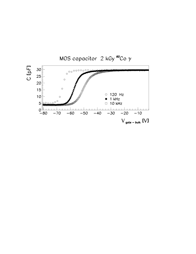
The observed frequency dependence is caused by the response of interface states to the AC signal, which depends on their position in the band gap. With increasing frequency these interface traps are unable to follow the AC swing [13].
A change in the hole mobility was observed after irradiation with 2.8 kGy 60Co photons: from cm2/(V s) to cm2/(V s).
A shift in the flatband voltage has been observed in the gate controlled diode I/V characteristics.

Figure 25 shows the I/V characteristics of two gate controlled diodes exposed to 50 Gy and 2.8 kGy, respectively, compared to the curve of an non irradiated diode. Flatband voltages V and V are roughly estimated for the two irradiation doses. The values correspond to the gate voltages at half of the maximum current value. The shape of the I/V curves are deformed after irradiation. The deformation is caused by the radiation induced change in the correlation between gate voltage and silicon surface band bending [21]. A strong increase of the surface current is detected. The surface current after irradiation is estimated as the difference between the maximum current value and the inversion plateau at large negative gate voltages. It increases from 6 pA (2 nA/cm2) for the non irradiadiated diode to about 300 pA (86 nA/cm2) after 50 Gy. After 2.8 kGy it is about 7 nA (2 A/cm2). The results are summarized in table 3, where flatband voltages, surface currents and surface recombination velocities are reported.
| Dose (Gy) | (nA/cm2) | cm/s | |
|---|---|---|---|
| 0 | -8.7 | 2 | 1.5 |
| 50 | -15 | 86 | 64 |
| 2800 | -60 | 2000 | 1500 |
5 Summary
The construction phase of the ZEUS Micro Vertex Detector (MVD) has been completed. The MVD has been successfully installed in the ZEUS detector and it is ready for the first collisions of HERA II. An extensive test program has been performed to study the characteristics and performance of the sensors. In the following, a summary of the electrical measurements on prototype and series production sensors is presented:
-
•
Resistivity of Si-crystals, kcm, corresponding to depletion voltages of the sensors V.
-
•
Low leakage currents, typically below 1 nA/cm2.
-
•
The stability of the leakage current has been tested for at least 24 hours at a bias voltage V. The fraction of stable sensors is 99%.
-
•
Coupling capacitance pF/cm, while the interstrip and backplane capacitances are pF/cm and pF/cm, respectively.
-
•
The values of the poly-Si resistors, used to bias the strips, are between M; the and aluminum strip resistances are 90 k/cm (W14), 100 k/cm (W12), and /cm, respectively.
-
•
The interstrip isolation has been verified and shown high interstrip resistances ( G cm) up to 10 V interstrip potential difference for a fully depleted sensor.
-
•
The mobility of holes in the interface has been estimated to be cm2/(V s).
The values of depletion voltage and of leakage current after
neutron irradiation are in agreement with the prediction from the
Hamburg model of hadronic irradiation [18, 19].
For fluences up to 1 MeV eq. n/cm2
(much higher than the hadronic background expected during the MVD lifetime),
type inversion has not occurred and the influence of hadronic irradiation is
limited to a change in the depletion voltage and an increase of the
bulk generation current.
A large increase in the leakage current has been found also for 60Co
photon irradiation. The increase after floating irradiation was a factor of 10
lower than for the biased irradiation. The increase in leakage current
is attributed to additional
generation currents in the SiO2 - Si interface.
A large shift in the flatband voltage has been observed,
corresponding to positive charges in the oxide and
interface areas.
A decrease in the hole mobility has been measured using the PMOS transistor.
References
- [1] U. Schneekloth (editor), “The HERA Luminosity Upgrade”, DESY internal report, DESY-HERA 98-05, 1998.
- [2] ZEUS Collaboration, M. Derrick et al., The ZEUS Detector, Status Report 1993, DESY, 1993.
- [3] ZEUS Collaboration, M. Derrick at al., Z. Phys. C 74 (1997) 207.
- [4] M. Feuerstack-Raible, Nucl. Instr. and Meth. A 447 (2000) 35.
-
[5]
V. Chiochia, “The ZEUS Micro Vertex Detector”,
proceedings of the Vertex 2002 conference, hep-ex/0111061,
submitted to NIM A.
E. Koffeman, Nucl. Instr. and Meth. A 473 (2001) 26.
M. C. Petruccci, Int. J. Mod. Phys. A Vol. 16 Suppl. 1C (2001) 1078.
U. Kötz, Nucl. Instr. and Meth. A 461 (2001) 210.
A. Garfagnini and U. Kötz, Nucl. Instr. and Meth. A 461 (2001) 158.
E. Koffeman, Nucl. Instr. and Meth. A 453 (2000) 59.
C. Coldewey, Nucl. Instr. and Meth. A 453 (2000) 149.
C. Coldewey, Nucl. Instr. and Meth. A 447 (2000) 44.
R. Klanner, “The ZEUS Micro Vertex Detectror”, proceedings of the International Europhysics Conference on High Energy Physics, EPS-HEP 99, Tampere, Finland.
A. Garfagnini, Nucl. Instr. and Meth. A 435 (1999) 34. - [6] D. Dannheim, Diploma Thesis, Hamburg University, DESY THESIS-1999-027.
- [7] J. Martens, Diploma Thesis, Hamburg University, DESY THESIS-1999-044.
- [8] Hamamatsu Photonics K.K., Japan.
- [9] U. Kötz et al., Nucl. Instr. and Meth. A 235 (1985) 481.
- [10] A.S.Grove, “Physics and technology of semiconductor devices”, John Wiley & Sons, New York, 1967.
- [11] Keithley Instruments Inc., USA (http://www.keithley.com).
- [12] Agilent Technologies, USA. (http://www.agilent.com).
- [13] E. H. Nicollian and J. R. Brews, “MOS physics and technology”, John Wiley & Sons, 1982.
- [14] G. Lindström, M. Moll and E. Fretwurst, Nucl. Instr. and Meth. A 426 (1999) 1.
- [15] Hamamatsu Photonics K.K., private communications.
- [16] T. Johnsen, PhD Thesis, Bergen University, 1994.
- [17] D. Pitzl, et al.,Nucl. Instr. and Meth. A 454 (2000) 334.
- [18] M. Moll, PhD Thesis, Hamburg University, DESY THESIS-1999-040.
- [19] G. Lindström et al., RD48 (ROSE) Collab., Nucl. Instr. and Meth. A 466 (2001) 308.
- [20] A. Longoni, et al., Nucl. Instr. and Meth. A 288 (1990) 35.
- [21] Jens Wüstenfeld. PhD Thesis, Dortmund University. UniDo-PH-E4-01-06, 2001.