Radiation Hardness and Linearity Studies of CVD Diamonds
Abstract
We report on the behavior of CVD diamonds under intense electromagnetic radiation and on the response of the detector to high density of deposited energy. Diamonds have been found to remain unaffected after doses of 10 MGy of MeV-range photons and the diamond response to energy depositions of up to 250 GeV / cm3 has been found to be linear to better than 2 %. These observations make diamond an attractive detector material for a calorimeter in the very forward region of the detector proposed for TESLA.
1 Introduction
With the establishment of the Chemical Vapor Deposition (CVD) growth
processes, diamond detectors started to be extensively investigated
for their use for particle detection at future high energy and nuclear
physics experiments. The developments were driven by the need for a
radiation detector, particularly at the upcoming generation of
experiments at hadron colliders like the Large Hadron Collider
(LHC). The main problem diamond is faced with is its small charge
collection efficiency, resulting in bad signal to noise ratios. Most
of the studies, focused on the hadronic radiation hardness properties,
have shown that diamond detectors suffer some radiation damage for
fluences of neutrons, protons or pions above approximately
/cm2 [1].
At a possible future high energy
electron positron collider like TESLA [2], the detectors
in the very forward region are subjected to very high radiation doses,
mostly electromagnetic radiation produced as beamstrahlung. Doses as
high as several MGy per year are expected. Recently a number of
studies have been published on the use of diamond in these regions as
a possible detector material [3].
In this paper, after a
description of the principle of operation of diamonds and the
definition of some important parameters, we summarize the results
concerning the radiation hardness, the Thermally Stimulated Current
measurements (TSC) and the linearity tests.
2 Principle of Operation
Diamond has a number of properties which make it an attractive
material for use in particle detection applications. The ionization
produced by energetic charged particles passing through a thin diamond
film, typically of the order of 300-500 m thick, creates about 36
electron-hole pairs per of diamond. By applying a potential
difference (typically 1V/) between the two electric contacts
the charges start to migrate toward them. Due to impurities and
dislocations in the diamond, some of the migrating charges are trapped
and may contribute to space charge, which builds up and polarizes the
diamond crystal. The charge induced on the contacts is then smaller than the total charge created in the
diamond .
A widely used figure of merit of the
diamond material is its charge collection efficiency defined as
. For current
diamond material the charge collection efficiency is typically below
.
If the diamond is exposed to high levels of ionizing radiation,
additional defect may be created in the diamond lattice, which may
trap charge. These defects may be caused by impurities in
the material (e.g. Nitrogen) or by structural damage to the lattice
(e.g. dislocations, etc.). Several methods exist to study the defects
and to better understand the mechanism of charge trapping in diamond. A
particular powerful method one is the method of Thermally Stimulated
Current (TSC). In this method, after having filled the traps at room
temperature, the diamond is heated up. The rise of the sample
temperature induces thermal detraping at a rate depending on the
temperature and on the energy levels of the traps. A current
proportional to the trap density and to the release rate is then
observed between the contacts of the diamond sample. The TSC
dependence on the temperature gives information about the energy
levels and the density of the impurities in the diamond.
In
addition to maintaining a good charge collection efficiency, a
detector to be used in a high radiation rate environment also has to
show a linear response to large energy deposition. This is
particularly important for the application of this material in a
possible forward detector at a linear collider, where energy deposits
over many orders of magnitude are to be expected.
In the following sections, we summarize studies and present results
for both radiation and linearity issues for diamond detectors. For a
more detailed description of the analysis see reference [3].
3 Radiation Hardness
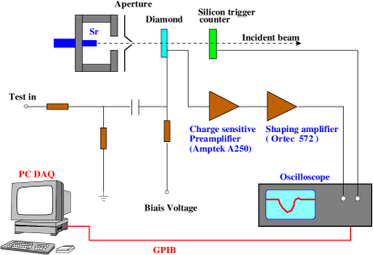
The response of CVD diamonds to uniform ionization densities has been measured using the setup shown in figure 1. The diamond samples were metalized with Ti/Pt/Au electrodes on both sides and placed in front of a collimated 90Sr source which delivers electrons up to a maximum energy of 2.28 MeV. In order to guarantee that only signals from 90Sr decay electrons which penetrate the diamond are recorded, a silicon trigger counter is placed behind the diamond sensor. The diamond signal is amplified using a charge integration amplifier circuit and can be viewed on a digital scope or recorded on a computer for future analysis. From the measured charge, one can estimate the charge collection efficiency.

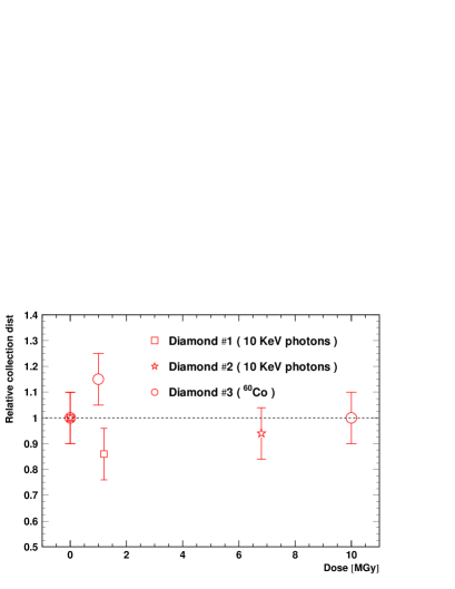
Three Diamond samples were exposed to electromagnetic radiation with two different ranges: below and above the threshold for non ionizing damages. A 10 KeV photon beam provided by the Hasylab facility at DESY with an average dose rate of 14 Gy/s was used to irradiate two diamond samples for doses up to 1.6 and 6.8 MGy. A third diamond sample was sent to a 60Co irradiation facility which provides photons with energies of 1.17 and 1.33 MeV. The diamond sample was irradiated with a dose of 10 MGy.

Figure 2 show the total relative charge collection efficiency for the three diamond samples for different irradiation doses. No indication of degradation of the diamond quality as a function of the radiation dose has been observed.
4 Thermally Stimulated Current
Using the TSC method several diamond samples have been studied for
their defect structure. After irradiation the samples were exposed to photons from a weak 10 KeV source to create electron-hole pairs in the sample.
To measure the TSC, a nominal voltage of 50 V
was applied on one contact of the diamond during measurement and
irradiation periods. The other contact was connected to a Keithley
6514 nano-A meter to measure the current. To generate the TSC, a
remote-controlled heating element was used. The temperature was
monitored using a thermocouple element read by a voltmeter.
Before heating the diamond, a fixed period of irradiation was used to
create electron-hole pairs in the diamond and fill traps. For this
purpose, the 10 KeV photon beam was directed on a 100 100
m2 slit. A remote-controlled shutter was placed between the
detector and the slit to switch the beam on and off between data
taking periods. For each acquisition sequence, an irradiation period
of 60 s, well below the time period over which saturation effects
become important, was done before the TSC curve was recorded. To study
the influence of different areas on the diamond on the measurement an
area of 1 mm2 was scanned in steps of 100 100
m2.
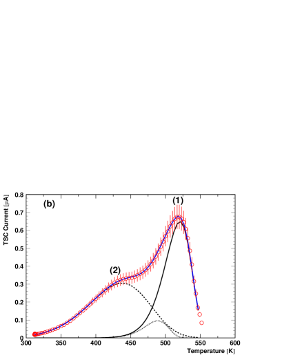
Figure 3 shows a sample TSC curve of the
evolution of the measured current with temperature. A fit to the TSC
curves was performed to evaluate the energy levels, the frequency
factors and the total density of traps. The deconvolution analysis
yields to two energy levels equal to 0.35 and 1.19 eV.

5 Response Linearity
The linearity of the response of the diamond detector was tested using
the Hasylab synchrotron radiation facility at DESY. A diamond detector
was placed in a 10 KeV photon beam which was intense enough to provide a high energy density
two orders of magnitude larger than what is expected at the TESLA Luminometer.
The beam intensity was about 2000 photons per bunch on a
m2 area. The beam was shone on a diamond
surface of about 1 mm2, defined by a copper mask.
The photon flux on the detector for the maximum beam
current (about 80 mA) corresponds to a deposited energy
density in the diamond of about 7.5 GeV/cm2 for a 300 m
thick diamond.
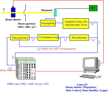
Figure 4 shows a sketch of the experimental setup used for the linearity studies.
The diamond detector was read out using an
Amptek A250
pre-amplifier, that was
followed by an Ortec amplifier/shaper with a 50 ns shaping time.
The output signal of the amplifier/shaper was sent to a Lecroy 1182 ADC.

Figure 5 shows the variation of the measured
signal as a function of the energy density in the diamond. One can clearly notice the linear relationship between the energy deposited in the diamond detector and the total collected charge. For low energy densities, one sees a non-linear behavior, ascribed to the pedestal. The bottom plot on figure 5 shows the
relative difference (ADC counts)/(ADC counts) between the data
and the linear fit to these data.
These measurements show that
the diamond detector is linear to better than 2% up to 7.5 GeV/cm2
for a detector thickness of 300 m.

6 Conclusions
Properties of CVD diamond detectors like their radiation hardness, their characterization using the TSC method and their linearity response to large amount of electromagnetic deposited energy, have been studied. Diamonds detectors have been found to exhibit a linear response to better than 2% for energy depositions of up to 250 GeV / cm3.
References
- [1] D. Meier, Ph.D. thesis, Universität Heidelberg, 1999; A. Oh, Ph.D. thesis, Universität Hamburg, 1999; Z. Zhao, Ph.D. thesis, Ohio State University, 1994.
- [2] TESLA Technical Design Report, Part IV: A Detector for TESLA, editors: T.Behnke, S. Bertolucci, R.-D. Heuer, R. Settles, 2001.
- [3] T. Behnke et al., hep-ex/0108038, Nucl.Instrum.Meth. A489 (2002); T. Behnke et al., LC-DET-2002-001.