The Power Supply System of the CLEO III Silicon Detector
Abstract
The CLEO III detector has recently commenced data taking at the Cornell electron Storage Ring (CESR). One important component of this detector is a 4 layer double-sided silicon tracker with 93% solid angle coverage. This detector ranges in size and number of readout channels between the LEP and LHC silicon detectors. In order to reach the detector performance goals of signal-to-noise ratios greater than 15:1 low noise front-end electronics together with highly regulated low noise power supplies were used. In this paper we describe the low-noise power supply system and associated monitoring and safety features used by the CLEO III silicon tracker.
PACS: 29.40.Wk; 84.30.Jc
Keywords: CLEO; Silicon; Microstrip; Power
Corresponding author.
E-mail address: kass@ohstpy.mps.ohio-state.edu,
1 Introduction
The CLEO III experiment[1] is located at the Cornell Electron Storage Ring (CESR), a symmetric e+e- collider operating in the energy range ( 10.5 GeV). It provides access to a rich variety of -meson, tau and charm physics topics. CLEO III is the third major upgrade of the CLEO experiment in the past twenty years. This upgrade had several goals including improving the particle identification capabilities to insure separation over the entire range of momenta expected from -meson decay, replacement of the charged particle tracking system as most of its elements were more than a decade old, and a new data acquisition system to accommodate the expected increase in CESR luminosity and new detector systems. Several important elements of the CLEO II detector were kept for use in CLEO III. These elements included the CsI calorimeter, 1.5T superconducting magnet, and the muon detector system.
In order to create sufficient space inside the magnet volume for a Ring Image CHerenkov (RICH) detector the radius of the charged particle tracking system was reduced from CLEO II’s 1 meter to 0.8 meter. One of the challenges of the CLEO III tracking system was to provide the same momentum resolution as CLEO II’s but use a smaller region of space. To meet this challenge a new silicon detector and wire drift chamber were designed and fabricated. In this paper we first describe the CLEO III silicon detector and then provide details on the power supply system used to operate it.
2 CLEO III Silicon Detector
The CLEO III silicon detector has been been described in detail in previous publications [2, 3, 4, 5]. Here we briefly review its design. The CLEO III silicon detector consists of 4 layers of double-sided silicon microstrip sensors that form barrels around the beampipe. A total of 447 identical sensors are daisy-chained into 61 ladders that are read out on both ends. Each of the 122 readout chains consists of sensors, a pair of flex cables, a hybrid board that hosts resistor/capacitor (RC), frontend amplifier (FE) and backend digitizer (BE) chips (Fig. 1), a portcard, and subsequent VME readout and control boards.

The sensors are DC coupled; bias resistors and AC coupling capacitors are located on separate chips (RC). Each sensor contains 511 strips and 511 strips. Thus there are 125 readout channels in the CLEO III silicon detector. Three voltages, Nstrip, Pstrip, and Pstop, are necessary to bias the sensors. The Nstrip and Pstrip voltages deplete the sensor bulk. The Pstop voltage biases “atolls” around the strips on the n-side and thus reduces the capacitance and supports the depletion process. The sensors are oriented such that the p-strips measure the coordinate (parallel to the beam axis) while the n-strips measure the coordinate.
To minimize tracking uncertainties due to multiple scattering the mass of the detector was made as low as possible (radiation length 1.6%). To achieve this end, the detector readout electronics are not in the tracking volume but at the ends of the ladders. Thus most of the radiation length is due to the silicon sensors. In order to achieve good tracking efficiency a signal to noise ratio of in all layers is desired. However, due to the considerable length of the sensor ladders, up to five sensors are ganged together, low noise front-end electronics and low detector capacitance are required to achieve this signal-to-noise goal. The frontend electronics chips are located on hybrid boards that are mounted outside the active tracking volume on the mechanical support cones. Two flexible (“flex”) cables are used to connect n and p-side readout strips of the sensor to the hybrid. The flex design uses two metal layers patterned with traces on both sides of a 25 kapton substrate [6].
BeO was chosen to be the hybrid substrate due to its excellent thermal and mechanical properties. Each hybrid has four RC, FE, and BE chips on the top and bottom surfaces as well as bypass capacitors, resistors for the chip voltages, a temperature monitor circuit, and two connectors for power and data lines. Each RC chip hosts 128 bias resistors and AC coupling capacitors on a 500 m thick quartz substrate. Due to the common ground for n and p-side electronics the voltage across the coupling capacitor is about half the depletion voltage. This is well below the measured RC breakdown voltage which is in the range of 75 - 100 V. The FE chip consists of a preamplifier, a CR-RC shaper, and a variable gain stage. A 5V supply (AVDD) and a 2.5V supply (AVDD2) are used to operate the FE chip. Amplified signals from the FE chips are transferred to the BE chips for digitization. The BE chip is a modified version of the LBNL SVX2b design[7]. Each BE chip hosts 128 8-bit Wilkinson ADC’s, comparators and a First-In-First-Out (FIFO) buffer. The comparators allow for sparsified readout. The BE chip is powered by a 5V supply (DVDD). Most of the power consumed by the silicon detector, up to 4 Watts per hybrid, is generated by the electronics on the hybrids. The heat generated on the hybrid is transferred to the support cones through a copper post on the hybrid.
Signals and supply voltages are routed to the hybrid through intermediate boards called portcards. The portcards are located in eight crescent-shaped crates that form full rings around the beampipe. These cards are located about 1 meter away from the interaction region. Each crescent crate contains up to 16 portcards and one buffer card that serves as a signal repeater for CLEO III slow control signals. The portcards host the ADC’s and DAC’s used by the slow control system. These cards are powered by a 5V supply (V5PC) and a 6V supply (V6PC). The 6V supply is used to generate low current voltages that supplement the FE and BE chips supply voltages. The readout chains terminate in VME based data boards equipped with a BE chip readout sequencer, data FIFOs and a digital signal processor for formatting the data. Each data board services four readout chains.
The slow control process resides in a MVME 2432 CPU [8] inside the master slow control crate. This crate also contains the interface boards necessary to control the portcards. Two VME repeater boards located in the same crate communicate with corresponding repeater boards in the two power supply crates. This setup with only one slow control process residing in one crate CPU makes powering the silicon detector almost independent of computer network problems and simplifies the slow control program structure.
| Voltage | Description | Voltage | Total Current | |
|---|---|---|---|---|
| Name | (Volts) | (Amps) | Control | |
| Nstrip | Sensor n-side bias | 50 | DAC | |
| Pstop | n-side barrier | 35 | DAC | |
| Pstrip | Sensor p-side bias | -50 | DAC | |
| V5PC | Portcard Supply | 5.0 | 0.15 | Switch |
| V6PC | BE/FE currents | 6.0 | 0.1 | Switch |
| AVDD | FE chip supply | 5.0 | 0.25 | Switch |
| AVDD2 | FE chip preAmp+shaper | 2.5 | 0.1-0.8 | Switch |
| DVDD | BE chip supply | 5.0 | 0.1 | Switch |
| V5PISO | PS card analog | 5.0 | – | – |
| V12+ | PS card analog | 12.0 | – | – |
| V12- | PS card analog | -12.0 | – | – |
| VME +5 | PS card VME | 5.0 | 0.2 | monitor card |
3 CLEO III Silicon Power Supply System
3.1 Silicon Power Supply System Overview
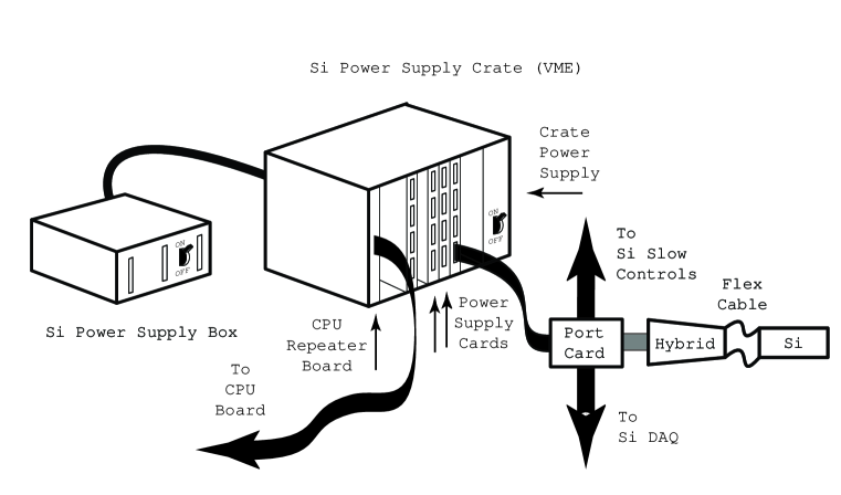
The CLEO III power supply system provides the voltages to each of the above subsystems in an integrated fashion. The CLEO III power supply system consists of two modified VME crates, six power supply boxes, thirty four power supply cards and software. The power supply cards, boxes and the J3 VME backplanes were custom designed to meet the needs of the CLEO III silicon project. In addition to the specialized hardware, software has been developed specific for the power supply cards and boxes and for communications between the power supply system and the rest of the CLEO III experiment. A diagram with the principal power supply system components is given in Fig. 2 In the sections below we describe each of these components in detail.
3.2 Power Supply Boxes
A power supply box contains the DC power supplies necessary to operate the the portcard, the hybrid, and the analog section of the power supply card as well as those necessary to bias the detector and monitor the status of the supplies. Linear power supplies[9] chosen for their excellent noise performance are used to power the silicon detector. There are 9 supplies inside each box. This relatively large number of supplies results from our decision to use separate supplies for digital and analog sections of the hybrid and portcard. This prevents noise coupling through common power leads. All supplies are floating at the supply end, ground is at the detector. All supplies are current limited and over-voltage protected. Each box can supply up to 28 hybrids (7 power supply cards). The entire silicon detector is powered by 6 boxes, three on the east and three on the west side of the detector. One box on each side services hybrids in layers 1 and 2, one box layer 3 hybrids and one box layer 4 hybrids.
A power supply box can be controlled either through an internal monitor card, driven by an RS485 serial line, or by front panel switches. The monitor card also records the temperature of the supplies and voltage levels at the power supply box output. In remote mode these voltages and temperatures are compared with programmable upper and lower limits and if a supply is out of bounds a relay is activated that shuts the supply off.
Each box can consume up to 200 Watts. Much of the power is transformed into heat inside the box. Since the power supply box is a closed system the heat can not be taken out by circulating air alone. The heat is taken out via copper plates and water cooling lines on the top and bottom of the box. Two fans inside the box increase air circulation and improve the cooling of the power supplies. Studies using 15.6oC water flowing at 1.5 liters/min through the bottom and top copper plates show that the ambient temperature inside the box stays well below 50oC at full load.
The boxes are located about 2 meters away from the power supply crates. Each power supply box is connected to the back of a power supply crate by 36 cables. All cables are attached to the back of the power supply box. Of the 36 cables 20 are current carrying and 16 are for remote sensing. All voltages except the power supply card supply voltages (5V, +/- 12V) are remote sensed at the back of the power supply crate. A power supply box weighs about 150 pounds (68 kg) and is operated with 208 V AC.
Before installation into the CLEO III experiment each power supply box was required to operate continuously at 120% load for at least three days. No power supply failures or cooling related problems have been observed during the first six months of operation of the silicon detector.
3.3 Power Supply Crates
There are two power supply crates in the CLEO III silicon detector system. These are 9U VME crates with a custom J3 backplane. Cables from the back of the power supply boxes terminate in connectors that plug into a custom-made J3 backplane. This backplane has a row of J3 connectors attached on the inside of the crate. Each VME crate contains 17 power supply cards and a VME repeater card. The repeater card and VME section of the power supply cards are powered by 5V, high current, high frequency switching power supplies[10] that are located inside the VME crates. This voltage is controlled by a monitor board that allows remote switching of the VME 5 V. The monitor board also interlocks the crate power to the cooling system of the crates and of the silicon detector. The VME crates are water-cooled. The system is designed such that all power transfer to the detector is shutdown in a controlled fashion when a cooling interlock is broken or the crates are turned off.
3.4 Power Supply Cards
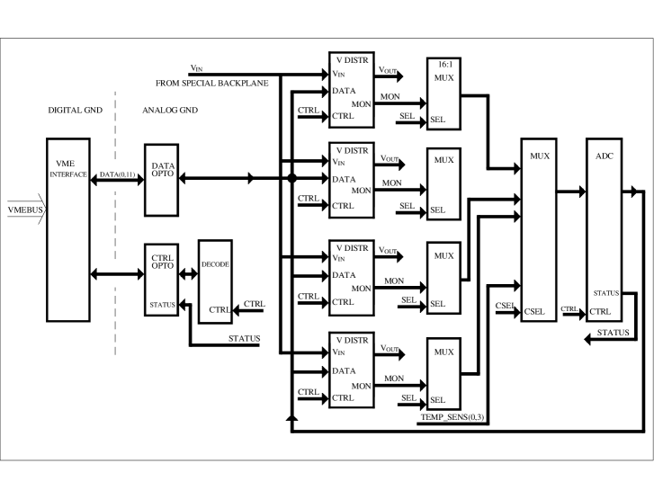
The power supply cards distribute the voltages necessary to operate the silicon detector in a fashion consistent with its low noise goals. For safety reasons each card also monitors, using a single 12 bit ADC, the relevant voltages, currents, and temperatures. Should a voltage, current, or temperature exceed its onboard programmable limit (upper or lower) the card will automatically trip the offending supply circuit and send a message to the CLEO III control system. The power supply cards reside in the power supply crates. There are 34 cards in the entire system, with 17 in each crate. Each card is divided into a digital VME part and an analog part. The analog part is subdivided into four identical sections with each section servicing one detector readout chain. Power comes in through the J3 VME connector and is distributed to the four sections. Each section is connected to a portcard, approximately twenty five feet away, via a 50 conductor flat cable [11]. In order to minimize voltage losses due to the resistance of the cable conductors a fifty foot length of cable is folded in half and the portcard connector is put in the middle of the cable and power supply card connectors on each of the cable ends.
3.4.1 VME and control section of power supply card
The power supply cards communicate with the rest of the experiment using the VME protocol. The VME section of each card consists of VME buffer chips, an ALTERA 10K-30 chip (onboard state machine), and a 30MHz oscillator to clock the state machine. The state machine controls ADC and DAC functions and performs on-board functions through VME commands. An independent state machine process performs voltage, current and temperature monitoring tasks. The state machine program is described in the next section. The VME section is powered by a dedicated 5 V supply located in the power supply crate.
Because this supply is a switching supply, it is isolated from the voltages that go out to the hybrids in order not to compromise the noise performance of the detector. The board state machine exchanges signals with the analog section on the card through electrically isolated optocoupler chips. This electrically isolates the VME section from the rest of the board. The DAC settings and ADC values are transferred on a 12 bit bi-directional data bus. The control and status signals are unidirectional.
There are 32 switches, 12 ADC lines, 8 DAC lines, and 10 select lines on a power supply card. In order to save space on the card a design with two address busses (CSEL(0:3), SEL(0:5)) and programmable decoder chips [12] was chosen. Each switch or DAC-select line is identified by a unique set of address words. The address values are decoded by four programmable decoder chips that provide the switch-select and DAC-select signals for one section.
Signals are routed from the analog section of the board to the ADC via a series of multiplexers.The multiplexers are controlled by the same address lines as the DAC’s and decoder chips. The address space has been divided between multiplexer and decoder functions so that the multiplexer can be operated without activating the decoder chips and vice versa. A schematic view of this system is given in Fig. 3.
3.4.2 Analog section of power supply card
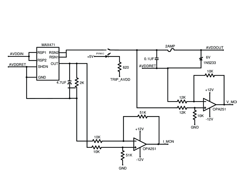
Each card contains four identical analog sections. The analog sections of the board distribute the voltages to the portcards, hybrids and sensors, host the on-off switching network for the portcards (V5PC, V6PC) and hybrids (AVDD, DVDD, AVDD2), the bias voltage (Nstrip, Pstrip, Pstop) circuits, and hybrid temperature monitoring circuits. In Fig. 4 the circuit used for the AVDD, the analog +5V supply, is shown.
The MAX471, shown in Fig. 4 is a high side current monitor. It mirrors the high side to a ground referenced current. It introduces a series resistance of 0.07 . The PVN012 is a solid state switch with an on resistance of 0.04 . The voltage difference between the power lead and the return line is monitored. Both the current and the resistance of the power leads are known, thus the voltage at the load can be calculated. The result is a software remote sense. This circuit is representative of the ones used for DVDD, AVDD2, V5PC, and V6PC.
The three bias voltages (Nstrip, Pstrip, Pstop) are generated on the power supply board from the 60 V power supplies located in the power supply boxes. The schematics for these circuits are shown in Figs. 5, 6, and 7 respectively. The typical operating values for these voltages are given in Table 1. The circuit designs for the three voltages are similar. The output voltage is controlled by a DAC; voltages and currents are measured by similar circuits. The bias voltage can be ramped in steps of 0.2 V. Sudden large bias voltage changes from () a power outage can in principle damage the RC chips. To protect against this situation the bias circuits provide a 2 second settling time without adding a large series resistance to the output.
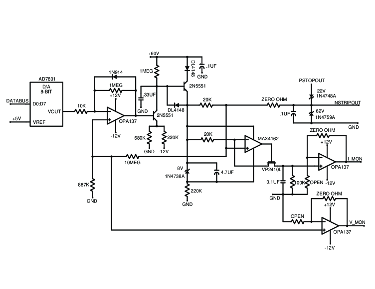
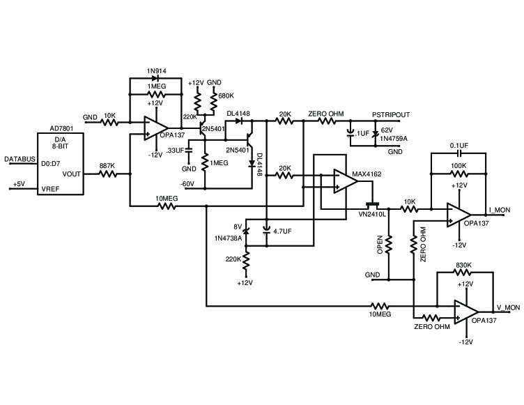
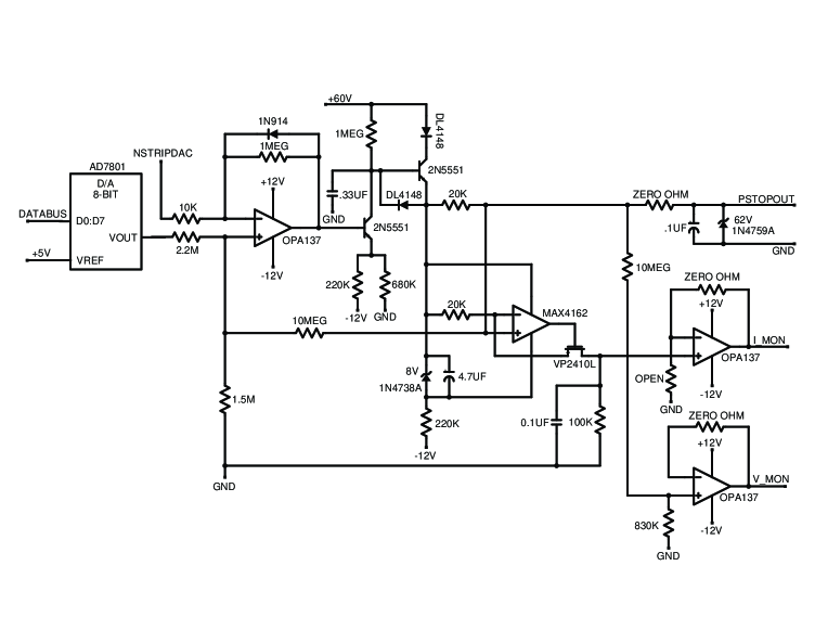
The analog sections that read the current and voltage levels have been designed to conform to the low noise requirements of the silicon detector. Each of these sections transforms and/or buffers the analog input into a voltage that can be digitized by the ADC. A total of 68 values are read by the board and transferred to the ADC through the two analog multiplexer (MUX) levels. Each analog section has one 16-input MUX for 8 voltage and 8 current channels. The section multiplexer passes signals on to the top-level MUX. The top level MUX selects the ADC input from the four section multiplexer outputs. The hybrid temperature channels do not fit into the section multiplexer and are directly connected to the top-level MUX.
All hybrid and portcard voltage lines are protected by fuses on the power supply card. The fuse ratings are limited by a second set of fuses on the portcards, which are less accessible. Therefore fuse ratings for the power supply card fuses were carefully chosen so that these fuses blow before the portcard fuses.
3.5 Power Supply Card Software
The power supply card state machine is programmed in AHDL [13] to perform the three main tasks described below. A general 32 bit register controls most of the features to be described, e.g. the timeout constant and the speed of the monitor process.
1.) Communicate with the CLEO III experiment via VME. The state machine interprets VME commands which are sent by the master slow control CPU. All DAC’s, ADC’s and switches can be operated remotely through these VME commands. The ADC readout has been made stable against short-time fluctuations by using the median value of five consecutive digitizations of an individual channel as the value returned to the slow control system.
2.) The program is equipped with a counter that measures the time of the last interaction with the slow control system. Each VME interaction resets the counter. If the counter reaches an externally adjustable value the state machine turns off all voltages controlled by this card. In current operation the timeout occurs after 2 minutes. The silicon detector has benefitted several times from this feature.
3.) A major part of the program is an independent readout loop that monitors all channels by digitizing the voltage, current and temperature values and comparing them to limits that are stored in internal registers. The comparison against lower limit values is also an option. In order to minimize readout fluctuations each channel is read out 4 times in a row and a limit is considered surpassed if 3 out of 4 readouts are above limit. During each readout loop the channels are compared against warning and trip levels. If a warning limit is surpassed a flag is set in an internal register and, if permitted by the slow control system, an interrupt is set. If a trip limit is surpassed the section is turned off and the address of the channel that caused the trip is stored in an internal register.
All limit registers are initialized automatically when the power supply cards are powered on. Each limit value can be updated externally. A readout loop consists of 272 digitizations and ADC readouts and takes a minimum of 3 msec. Most of this time is consumed by the digitization process. At this speed a small noise excess of the order of 100 e- ENC has been observed in the hybrid frontend electronics of the silicon detector. The speed of the monitor process can be slowed down externally in order to remove this noise which is caused by multiplexer switching. For readout loops longer than 500 msec no additional noise is introduced into the system. During normal operations the monitoring is performed with 1 sec long readout loops. In addition each channel is readout by slow control about every ten seconds.
A power supply card can also turn off the AVDD, AVDD2, DVDD, V5PC, V6PC, and bias supplies located in its corresponding power supply box. A buffered signal from the card’s state machine is brought from the front of the power supply card to the power supply box. This signal is daisy chained so that only one cable runs between the power supply cards and a power supply box.
3.6 Performance
The silicon detector has been taking physics quality data since July 2000 accumulating approximately 4.5 fb-1 of data to date. The silicon power supply system has proven to be stable in daily operations. Failures of system components have been almost exclusively restricted to fuses.
The frontend electronics has achieved its design goals. The single channel noise by layer ranges between 400 and 800 electrons. The z-side shows slightly lower noise than the -side due to the different sensor strip capacitances for n-side (=) and p-side (=z). The common-mode noise is of the order of 400 e- ENC. The noise values were obtained using the standard conversion of ADC counts to electrons which is known to about 20%.
Signal-to-noise ratios, which are independent of this calibration, were obtained from a high-statistics Bhabha sample recorded in summer 2000. Neighboring groups of channels above pedestal were merged into clusters. The sum of the pedestal-subtracted signals over all strips in a cluster was taken as the pulse height. Only clusters with 3 strips or less were considered. Tracks were restricted to a region of in order to select tracks with almost perpendicular incidence angle. The pulse height of silicon clusters associated to these tracks were divided by the channel noise averaged over all strips in the cluster. Loosening the cluster width or polar angle requirements increases the signal-to-noise ratios. Noise values and signal-to-noise (S:N) ratios for all 4 layers are given in Table 2.
| Layer | signal-to-noise | noise (100 e-) | ||
|---|---|---|---|---|
| r- | z | r- | z | |
| 1 | 27.9 | 34.4 | 6.1 | 6.1 |
| 2 | 29.9 | 37.4 | 5.9 | 4.4 |
| 3 | 19.4 | 27.3 | 8.2 | 5.7 |
| 4 | 20.1 | 22.6 | 8.2 | 6.5 |
4 Summary and Conclusions
The design and status of the power supply system of the CLEO III silicon detector has been presented in detail here. The silicon detector has been taking physics quality data since July 2000. The power supply system has been stable in daily operations. The noise performance of the silicon detector and its power supply system has been very good with 400-800 e- ENC common-mode subtracted noise. The frontend electronics has reached its signal-to-noise goals of better than 15:1 in all layers.
5 Acknowledgments
We would like to thank Vijay Sehgal for the excellent electronics shop support, Bob Wells for his help with the mechanical aspects of this project, and The Ohio State University’s physics department machine shop. This work was supported by the Alexander-von-Humboldt Stiftung, The Ohio State University, and the U. S. Department of Energy.
References
- [1] CLEO III Proposal CLNS94/1277 (unpublished). G. Viehhauser, Nucl. Instr. and Meth. A446 (2000) 97. T. Peddlar, to be published in the Proceedings of DPF2000.
- [2] E. von Toerne et al., Vertex2000 conference proceedings, to be published in Nucl. Instr. and Meth.
- [3] J. Fast et al., Nucl. Instr. and Meth. A435 (1999) 9.
- [4] I. Shipsey et al., Nucl. Instr. and Meth. A386 (1997) 37.
- [5] H. Kagan et al., Nucl. Instr. and Meth. A383 (1996) 189.
- [6] P. Skubic et al., Nucl. Instr. and Meth. A418 (1998) 40.
- [7] O. Milgrome et al., Nucl. Instr. and Meth. A383 (1996) 13.
- [8] MVME 2400, Motorola Computer Group, Tempe, AZ 85282.
- [9] Acopian Technical Company, Easton, PA 18044.
- [10] Vicor Corporation, Andover, MA 01810-5413.
- [11] The cable used is Beldon’s YP4465008. This is a 50 conductor, 30AWG flat cable with 25 mil pitch. Beldon Wire and Cable Company. P. O. Box 1980, Richmond, IN 47375.
- [12] XILINX, Inc., San Jose, CA 95124-3400.
- [13] Altera Hardware Description Language, Altera Corporation, San Jose, CA 95134.