Optical probe of electrostatic doping in an -type Mott insulator
Abstract
Electrostatic doping into an -type Mott insulator Sm2CuO4 has been successfully achieved with use of the heterojunction with an -type band semiconductor Nb-doped SrTiO3. The junction exhibits rectifying current-voltage characteristics due to the interface band discontinuity and the formation of depleted region. The application of reverse bias electric field on this junction enables the field-effect electron doping (presumably up to 6% per Cu atom) to the Mott insulator. The electro-modulation absorption spectroscopy could clearly show a large modification of the Mott-gap state accompanying the spectral weight transfer to the lower-energy region, reminiscent of formation of a metallic state.
pacs:
74.72.Jt, 78.20.Jq, 73.20.-rI Introduction
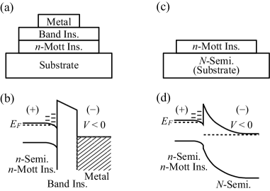
The electronic structure of parent Mott insulators and its dramatic modification with carrier doping, especially at the phase boundary, is of crucial importance for the fundamental understanding of the phase transition in strongly correlated electron materials imada . The electrostatic carrier doping is an attractive methods for such a study because it enables us a critical control of the carrier density without introducing randomness into the system. Usually, the electrostatic doping has been performed with use of the field-effect transistors (FETs) with metal-insulator-semiconductor (MIS) structures illustrated in Fig. 1(a)(b) newns ; ahn . In this structure, it is essential to prepare a high quality insulating film which should have large breakdown field and small leakage current to induce a change of carrier density (band filling) enough for the phase transition mis . However, a number of previous works have proved it technically difficult, while the problem of the leakage current could be partly overcome with using a ferroelectric compound as a gate insulator ahn ; ahn2 .
To overcome the difficulty, we adopt another scheme of field-effect device in this study, that is an isotype heterojunction comprised of a Mott insulator and a semiconductor (Fig. 1 (c)). A typical energy-band diagram of an (narrower-gap semiconductor)-(wider-gap semiconductor) isotype heterojunction as InGaAs/GaAs is shown in Fig. 1(d) capasso . Due to the difference in the chemical potential between these two contacting materials, the conduction-band discontinuity and band bending emerge at the interface. The band bending yields the charge depleted and accumulated regions at the interface. The self-formed depleted region works as a capacitor in such a junction, ensuring the high experimental reproducibility coupled with its simple device structure. The induced interface carrier density can be estimated from capacitance-voltage measurements. By replacing the narrow-gap semiconductor with an -type Mott insulator, it is expected to inject charge carriers into the Mott insulator with the field-effect. Here, “-type Mott insulator” means the Mott insulator in which the band filling can be increased to produce the conducting state, like -phase CuO4 (Pr, Nd, and Sm) known as the parent insulators of electron-doped high- superconductors.

In this Letter, we report on the electrostatic carrier doping to a Mott insulator and its optical detection in the heterojuncion comprised of Nb-doped SrTiO3 (Nb:STO) and Sm2CuO4 (SCO). The crystal structure of SCO is the so-called -phase composed of the alternate stack of fluorite-type Sm2O2 layers and CuO2 sheets with the lattice constant of Å and Å yang . Since the -axis lattice constant is close to that of STO (3.905 Å), a pseudomorphic interface is expected to reduce possible defects originating from the lattice mismatch. Nb:STO is an -type semiconductor with a band-gap of 3.2 eV. The energy-band diagram of the SCO/Nb:STO heterojunction was evaluated from current()-voltage() and capacitance()-voltage() measurements. As a method for the observation of the electrostatic carrier doping, we adopted the electro-absorption (EA) spectroscopy. This technique extracts only the modulated component in the absorption through the application of an electric field cardona . In the heterojunction, the field-induced absorption change would be limited in the vicinity of the interface. Thus, we expected that the EA spectroscopy serves as a sensitive probe of the injected carriers to the Mott insulator at the heterointerface. We stress here that the spectroscopic observation allows us to extract information on the variation of the electronic structure of the Mott insulator.
II Experiments
A 30 nm-thick SCO film was grown on a (100) Nb:STO substrate held at 780∘C in an oxygen pressure of 300 mTorr by pulsed-laser deposition, and the films was subsequently annealed to romove excess apical oxygens sawa . The sample should be semi-transparent so as to measure optical spectra in transmission geometry. Therefore, we employed a Nb 0.01 wt% doped STO (carrier density of 1 cm-3) as the substrate, which is almost transparent in the energy region of the visible light, although it has a metallic conductivity. X-ray diffraction measurements show that the film has a single-phase -axis oriented pseudomorphic structure ( Å). The lattice constants of the film are close to those of the bulk yang , signifying that the film is in -phase as expected.
To obtain an ohmic contact to the SCO and to apply an uniform electric field throughout the measurement area, semi-transparent Au film with a thickness of 6 nm was ex situ evaporated on top of the SCO film. The Au/SCO/Nb:STO junction was then patterned into a mesa-structure (the inset of Fig. 3) by photo-lithography, Ar ion milling, sputter coating of SiO2, and lift-off procedures. Finally, a 300 nm-thick Au film was deposited and patterned so as to work as the contact to the thinner Au film as well as lead wires. The size of the junction area is on which a monochromatic incident light was focused by an objective lens for spectroscopy. The base electrode was subsequently provided by depositing Al film which can form an ohmic contact to Nb:STO.
III Results and Discussion
The - characteristics of an SCO/Nb:STO junction is shown in Fig. 2 (on the left ordinate). The junction shows a rectification property without a breakdown up to a reverse bias of V. The rectification property indicates the existence of the band discontinuity and depleted region. Possible energy-band diagrams of SCO/Nb:STO junction is shown in the inset of Fig. 2 by analogy with a semiconductor - isotype heterojunction. The depletion length in Nb:STO reaches several hundreds nanometers in our case due to the large permittivity () and the small doping concentration. This rather simple rigid-band picture is strictly not the case for strongly correlated electron systems including Mott insulators in which the band reconstruction occurs with the carrier doping or with change of band filling. We believe, however, the conduction-band discontinuity and the formation of the depleted and accumulated regions are crucial to realize such rectification property in the SCO/Nb:STO heterojunction.
To obtain more quantitative information about the interface band discontinuity, we measured capacitance of the same junction. For an ideal - heterojunction, - characteristics is given by capasso
| (1) |
where , , and denote permittivity, carrier density, and diffusion potential, respectively, and the subscripts 1, 2 denote SCO and Nb:STO, respectively. If and , Eq. (1) can be approximated by forrest
| (2) |
Equation (2) is the same formula as that for a Schottky junction, and we can consider the band-offset on the analogy of that for a Schottky barrier. In Fig. 2 (on the right ordinate), we show a - curve measured at a frequency of 1 MHz. It is readily apparent that the plot of versus shows a linear relationship, indicating a small contribution from the trapped charges on the interface defects. is found to be 1.3 V from the voltage-axis intercept. It is difficult to deduce an accurate value of the conduction-band offset () because of a little information on the position of the Fermi energy relative to the conduction-band in SCO (). According to the result of x-ray photoemission spectroscopy for Nd1.85Ce0.15CuO4 taguchi , is so small as to assume that .

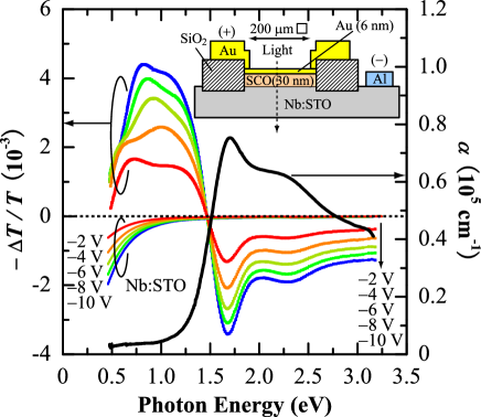
As illustrated in the inset of Fig. 2, the application of reverse bias should induce the accumulation of additional electrons in SCO at the interface in compensation for further exposed positive space-charge of ionized donors in depleted Nb:STO. The EA measurements were performed on the device with the configuration shown in the inset of Fig. 3. Rectangle wave electric field (570 Hz) with various reverse biases was applied to the specimen with a pulse generator. The semi-transparent area of the device was illuminated with a monochromatic light from a halogen or a xenon lamp, and the transmitted light was detected with a Si photodiode (1.1-3.2 eV) or an InAs photovoltaic detector (0.5-1.1 eV). The modulated component of the transmitted light () synchronized with the electric field was measured with a lock-in amplifier while monitoring the constant component (). The relation between and the change in the absorption induced by the electric field is approximated by , if , where is the absorption coefficient and is the thickness over which the spectral change occurs cardona .
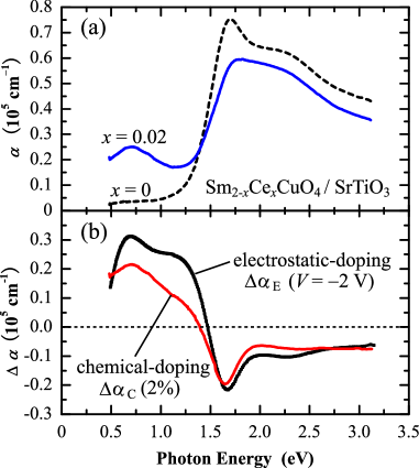
The optical absorption spectrum of a thin film of SCO is shown in Fig. 3 (on the right ordinate). The spectrum has a sharp absorption peak at 1.7 eV and a broad side peak at 2.2 eV, similarly to the bulk feature arima . The main absorption peak corresponds to the charge-transfer (CT) transition from the O 2 band to the Cu 3 upper Hubbard band (UHB) tokura2 , and its fairly sharp profile indicates the exitonic character of the transition. Within the CT gap, optical absorption is negligibly small. The EA spectra of the SCO/Nb:STO junction are shown in Fig. 3 (on the left ordinate). A very systematic enhancement of EA spectra is observed with increasing the amplitude of voltage modulation. At a first glance, one can notice that the spectra exhibit a sign reversal near the absorption-edge. The absorption increases () below the absorption-edge, whereas the CT absorption decreases () above that. To consider the origin of this feature, let us recall the effect of the carrier doping on the optical spectrum for under-doped -type cuprates. The previous studies with use of chemically doped bulk samples have revealed that the electron doping gives rise to the emergence of a new state within the CT gap and the suppression of the spectral weight in the higher energy region cooper ; uchida ; arima2 . For comparison, we also fabricated a 2% Ce doped (Sm1.98Ce0.02CuO4) thin film and measured the absorption spectrum as shown in Fig. 4(a). The close agreement of the EA spectra with the doping induced spectral change clearly indicates that the observed sign reversal in the EA spectra is a consequence of the field-effect electron doping in SCO. One might dispute that the EA spectra is caused by a low-energy shift of the absorption-edge, that would be the Franz-Keldysh effect as observed for semiconductors or band insulators cardona . If this were the case, the EA spectra would show substantial signals only near the absorption-edge and the oscillating structure of the EA spectra would show a large field dependence. However, we observed fairly large signals far below the absorption-edge, where no optical transition is observed in the linear absorption spectrum. Therefore, the influence of the red-shift of the absorption-edge is not a major source, if any. The existence of the isosbestic (equal-absorption) point at 1.47 eV is also an evidence of the transfer of the spectral weight from the CT absorption in a higher energy region to the in-gap absorption in a lower energy region.

Next, we discuss the spectral feature below the absorption-edge. As shown in the inset of Fig. 2, the application of reverse bias results not only in the accumulation of charges in SCO but also in the widening of the depleted region in Nb:STO. Therefore, the EA spectra should include the contribution from bleaching of free carrier absorption in Nb:STO. We estimated the Nb:STO contribution to the EA spectra from the quantity, . Here, and are absorption coefficients of non-doped STO and Nb:STO, respectively, and is the expanded depletion length by the applied electric field as deduced from the - measurement. As shown in Fig. 3, the contribution from Nb:STO is appreciable only below the mid-infrared region (), and the influence can be understood as a reduction of Drude-like free carrier absorption. Therefore, the spectral drop toward zero as observed in the lower energy region of the EA spectra may partly come from this bleaching effect of Nb:STO. By subtracting the Nb:STO contribution from the EA spectra, the field-effect contribution in SCO can be derived as shown in Fig. 4(b) (only the case of V is shown). After the subtraction, the feature of the spectral drop at lower energy still exists. We speculate that the drop may indicate the formation of the pseudogap originating from antiferromagnetic spin correlation as observed in the bulk under-doped Nd2-xCexCuO4 onose .
The carrier density injected by the electric field can be obtained from the equation, . The estimated is (0.020 electrons per unit cell area) at V and (0.063 electrons per unit cell area) at V. These values are comparable to the aforementioned carrier density attainable in the MIS structure. It is worth comparing the absorption changes induced by electrostatic-doping () and chemical-doping (), respectively, at the same doping level of 2%. is deduced from the EA spectrum obtained at V corrected by the contribution from Nb:STO, and assuming that the doping was effective only for a single CuO2 plane, , nm. was calculated from the difference of absorption spectra between Ce 2% doped SCO and undoped SCO. As shown in Fig. 4(b), the spectrum of has similar profile and magnitude with those of . The result ensures that the injected carriers are confined within quite narrow region, possibly in a single CuO2 plane adjacent to the interface. This interpretation is reasonable if one considers that the typical screening length in a Mott insulator is a few nanometers ohtomo ; okamoto and electron doped cuprates show quite a larger effective mass along the -axis direction than that within -plane beom .

IV Conclusions
We have detected the electric field induced change in electronic structure of a Mott insulator by an optical probe for a heterojunction comprised of Sm2CuO4 and Nb-doped SrTiO3, namely, an -type Mott insulator and an -type semiconductor. This junction exhibits a rectifying current-voltage characteristics due to the conduction-band discontinuity of about 1.3 eV as revealed by the capacitance-voltage measurement. The electro-absorption spectroscopy under reverse bias unraveled the collapse of charge-transfer gap and the emergence of in-gap states via electric-field doping of electrons in the top-most layer of Sm2CuO4. A concept of (Mott insulator)-(semiconductor) or (Mott insulator)-(semiconductor) isotype heterojunction is applicable as an effective carrier doping method to a wide range of Mott insulators. The interface-sensitive electro-modulation spectroscopy may quantitatively elucidate the electronic state of the Mott insulator at the heterointerface while continuously changing the doping level or band filling.
Acknowledgements.
We are grateful to H. Matsuzaki, Y. Okimoto, and T. Ogasawara for technical assistance, and to Y. Ogimoto, T. Hasegawa, and H. Okamoto for helpful discussions.References
- (1) M. Imada, A. Fujimori, and Y. Tokura, Rev. Mod. Phys. 70, 1039 (1998).
- (2) D. M. Newns, J. A. Misewich, C. C. Tsuei, A. Gupta, B. A. Scott, and A. Schrott, Appl. Phys. Lett. 73, 780 (1998).
- (3) C. H. Ahn, J.-M. Triscone, and J. Mannhart, Nature 424, 1015 (2003).
- (4) For example, when Al2O3 is used as the gate insulator, the estimated carrier density is 7.5 , corresponding to 0.07 electrons per the area of 1 unit cell squared of a perovskite oxide, under an electric field of 10 MV/cm.
- (5) C. H. Ahn, J.-M. Triscone, N. Archibald, M. Decroux, R. H. Hammond, T. H. Geballe, Ø. Fischer, and M. R. Beasley, Science 269, 373 (1995).
- (6) S. R. Forrest, in Heterojunction band discontinuities, edited by F. Capasso and G. Margaritondo (Elsevier Science, Netherlands, 1987).
- (7) H. D. Yang, T. H. Meen, and Y. C. Chen, Phys. Rev. B 48, 7720 (1993).
- (8) M. Cardona, Modulation spectroscopy (Academic, New York, 1969).
- (9) A. Sawa, M. Kawasaki, H. Takagi, and Y. Tokura, Phys. Rev. B 66, 014531 (2002).
- (10) S. R. Forrest and O. K. Kim, J. Appl. Phys. 52, 5838 (1981).
- (11) M. Taguchi et al., Phys. Rev. Lett. 95, 177002 (2005).
- (12) T. Arima, K. Kikuchi, M. Kasuya, S. Koshihara, Y. Tokura, T. Ido, and S. Uchida, Phys. Rev. B 44, 917 (1991).
- (13) Y. Tokura, S. Koshihara, T. Arima, H. Takagi, S. Ishibashi, T. Ido, and S. Uchida, Phys. Rev. B 41, 11657 (1990).
- (14) S. L. Cooper, G. A. Thomas, J. Orenstein, D. H. Rapkine, A. J. Millis, S-W. Cheong, A. S. Cooper, and Z. Fisk, Phys. Rev. B 41, 11605 (1990).
- (15) S. Uchida, T. Ido, H. Takagi, T. Arima, Y. Tokura, and S. Tajima, Phys. Rev. B 43, 7942 (1991).
- (16) T. Arima, Y. Tokura, and S. Uchida, Phys. Rev. B 48, 6597 (1993).
- (17) Y. Onose, Y. Taguchi, K. Ishizaka, and Y. Tokura Phys. Rev. Lett. 87, 217001 (2001).
- (18) A. Ohtomo, D. A. Muller, J. L. Grazul, and H. Y. Hwang, Nature 419, 378 (2002).
- (19) S. Okamoto and A. J. Millis, Phys. Rev. B 70, 075101 (2004).
- (20) Beom-hoan O and J. T. Markert, Phys. Rev. B 47, 8373 (1993).