Electronic structure of epitaxial graphene layers on SiC: effect of the substrate.
Abstract
Recent transport measurements on thin graphite films grown on SiC show large coherence lengths and anomalous integer quantum Hall effects expected for isolated graphene sheets. This is the case eventhough the layer-substrate epitaxy of these films implies a strong interface bond that should induce perturbations in the graphene electronic structure. Our DFT calculations confirm this strong substrate-graphite bond in the first adsorbed carbon layer that prevents any graphitic electronic properties for this layer. However, the graphitic nature of the film is recovered by the second and third absorbed layers. This effect is seen in both the (0001)and 4H SiC surfaces. We also present evidence of a charge transfer that depends on the interface geometry. It causes the graphene to be doped and gives rise to a gap opening at the Dirac point after 3 carbon layers are deposited in agreement with recent ARPES experiments (T.Ohta et al, Science 313 (2006) 951).
pacs:
73.20.At, 71.15.MbThe possibility of carbon nanotubes (CNT) switching devices has been pursued in the last decade because of their attractive electronic properties. Nevertheless, problems with large intrinsic resistance in contacts and the inability to control tube helicity, and thus whether or not they are metallic or semiconducting, have made large scale circuit designs problematic. The proposed solution to these problems is an all carbon nanoelectronics paradigm based on the planar 2D form of carbon, graphene.berger2
Graphene consists of a single carbon plane arranged on a honeycomb lattice. From a fundamental point of view, graphene ribbons can be seen as an unrolled CNT but with different boundary conditions (finite versus cyclic). Therefore, their electronic properties should be similar. In fact this has been demonstrated in recent experiments on single and multi-graphene sheets that show the existence of Dirac Fermions, large electron coherence lengths and anomalous integer quantum Hall effect berger ; novoselov ; zhang . The advantage of graphene over CNTs for electronics resides in its planar 2D structure that enables circuit design with standard lithography techniques. This enables the graphene to be cut with different shapes and selected edge direction. By simply selecting the ribbon edge direction it is possible to design metallic or semiconductor graphene ribbons edge ; edge2 (analogous to helicity in CNTs).
Since single or multiple sheets must be supported on a surface for fabrication, the pressing question becomes: how does the interface between a graphene sheet and its support affect its electronic properties? In other words can the symmetry of an isolated graphene sheet be maintained in the presence of an interface? It is this question that is the focus of this paper. Specifically we have studied the system of graphite grown on both polar faces of hexagonal SiC.
The graphene layers are produced by sublimating Si from either the 4H- or 6H-SiC (0001) (Si terminated) or (C terminated) surfaces at sufficiently high temperatures to graphitize the excess carbon forbeaux ; berger2 . 2D transport measurements on these graphitized surfaces show the presence of Dirac electrons similar to those found on exfoliated graphene berger ; novoselov ; rollings ; sadowski . Besides being a more practical and scalable approach to 2D graphene electronics, this system has the experimental advantage of having a well defined interface that can be characterized in contrast to mechanically exfoliated graphene flakes novoselov ; zhang that must in any case still be supported on a surface (usually ).
In this letter, we conclusively show that the first carbon layer grown above the SiC substrate has no graphitic electronic properties and acts as a buffer layer between the substrate and subsequent graphene layers. Atoms in this plane form strong covalent bonds with the SiC substrate. The next graphene layer above the buffer layer shows a graphene-like Dirac band structure expected for an isolated graphene sheet. The calculated results are consistent with a short C first plane-4HSiC substrate bond as determined by Surface X-ray Reflectivity. Under some conditions, charge transfer from the substrate results in a n type doping of the graphene layers (Fermi level above the Dirac point). This opens a gap in the graphene bilayer Dirac bands, in agreement with recent ARPES results ohta . Dangling bond related states are found in all tested geometries. These states can interact with the graphene derived state depending on the geometry. Their effects on the electronic and transport properties have to be considered as well as those of the intrinsic defects of the isolated graphene layer guinea .
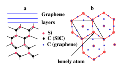
The systems theoretically studied here are made of one, two or three carbon layers (on a honeycomb lattice with Bernal stacking) on top of either a SiC 4H (0001) or (Si and C terminated) substrates. Graphene is nearly commensurate with these SiC surfaces with a common cell corresponding to a (with respect to SiC surface cell) forbeaux . This cell is too large to make realistic calculations. Even the next smallest nearest commensurate structure, cell (not experimentally observed), is too large for reasonable calculations. Therefore, as a first approximation to the actual structure, we used the reconstruction shown in Fig. 1. The cell corresponds to a graphene cell. The graphene and SiC lattice parameter mismatch requires an stretch of the graphene to make the two cells commensurate. We have checked that this expansion has no qualitative effect on a free standing graphene electronic structure (it will however change the Dirac electron velocity). The cell contains 3 atoms/layer in SiC. At the interface, two of these atoms are immediately below a C atom in the first C layer. The third atom (subsequently referred to as the ”lonely atom”) has no C atom above it. A bulk truncated 4H-SiC geometry was used on both faces. We have also checked another possible interface geometry based on surface X-ray scattering data: a C-terminated surface with one C atom out of three missing (referred to as ”C-deficient”). In the bulk truncated geometry, the lonely atom exhibits a dangling bond (DB) that points towards the graphene layers. The lonely atom is suppressed in the C-deficient geometry, thus creating 3 dangling bonds at the interface.
The electronic structure was investigated using the VASP code vasp . It is based on Density functional theory (DFT) within the generalized gradient approximation pw . The 4H SiC substrate is described with a slab that contains 8 SiC bi-layers with H saturated dangling bonds on the second surface. The empty space ranges from 15 to 25 Å. Ultra soft pseudopotentials uspp are used with a plane wave basis cutoff equal to 211 eV. The experimental graphene layer spacing was first chosen as the starting value and then all the atoms were allowed to relax. Since DFT is known to poorly describe Van der Waals forces, the final graphene layer spacing are significantly larger than in the bulk. However, we point out that the C-short ultrasoft pseudopotential used here has been extensively tested incze and was shown to correctly describe the band structure of graphite in spite of the larger layer spacings vdW ; evc . Integration over the Brillouin zone is performed on a 9x9x1 grid in the Monckhorst-Pack scheme to ensure convergence of the Kohn Sham eigenvalues. The K point is included since it is crucial to a good description of the Fermi level for a single graphene layer.
The X-ray experiments were performed at the Advanced Photon Source, Argonne National Laboratory, on the 6IDC-CAT Ultra High Vacuum scattering chamber. The C-Face samples were graphitized in a vacuum RF-induction furnace () x_ray and transported to the scattering chamber for analysis.
The calculations show that the relaxed geometry of the bulk layers is influenced only by the first carbon layer. Neither the bulk nor the first C layer are altered when subsequent C layers are added. In the last bilayer of the Si (C) terminated face the lonely atom is displaced toward the bulk by 0.3 Å (0.45), while the bilayer width remains globally unchanged (0.65 (0.7) compared to 0.62-0.63 in the bulk). The first graphene layer lies 2.0 (1.66) Å above the two outermost atoms. The second graphitic C plane is 3.8 Å (3.9) above the first one (subsequent planes are spaced by 3.9 Å). As mentionned above, the large value of the graphene interlayer spacings is due to the known difficulty of the DFT to describe the van der Waals force vdW ; evc . From these results, we deduce that the interface carbon layer strongly interacts with the SiC substrate for both Si and C terminated surfaces. Subsequent C-planes on the other hand are weakly bound by van der Waals forces as expected for graphite. This conclusion also holds for the C-deficient geometry. The bulk relaxation in this latter case is very similar to those of the C terminated bulk truncated geometry.
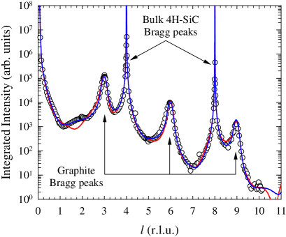
X-ray reflectivity data confirms this result. Figure. 2 shows an experimental reflectivity from graphene layer film grown on the 4H-SiC surface. Data is on the rod in units of , where . Peaks at and 8 are SiC Bragg reflections, while peaks at 3, 6 and 9 are graphite Bragg points. A full fit to the data including substrate relaxation and a multilayered graphite film is shown. Details of the fit are given in a separate article X-ray2 . The model consists of a single reconstructed SiC bi-layer interface between the graphite and the bulk. The fit reveals that the first graphene layer is above the last bulk C-layer consistent with the calculated value. The next graphene layer is separated from the first by (slightly larger than the bulk value Bulk_C ). Subsequent layers have a mean spacing of . This slightly larger layer spacing is consistent with stacking faults in the layers Faults . The x-ray results confirm the calculated structure of a strongly bonded first graphitic layer with a well isolated graphene layer above it. We note that the extended diamond interface phase conjectured by others forbeaux ; vanBommel75 does not fit the x-ray data for the C-face. This is demonstrated in Fig. 2 were we force a second SiC bi-layer to be Si depleted by . This fit is obviously worse than a single bi-layer and proves that the SiC interface is narrow and not extended.
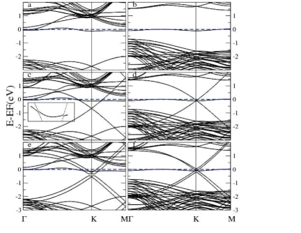
The band structures with one (Fig. 3(a) and (b)), two (Fig. 3(c) and (d)) and three (Fig. 3(e) and (f)) carbon layers on bulk terminated SiC are shown in Fig. 3. For both polarities, the electronic structure with a single C layer significantly differs from graphite mattausch . It exhibits a large gap and a Fermi level pinned by a state with a small dispersion (close to the conduction band for the Si terminated surface or in the gap for the C terminated surface). These states are related to the Dangling Bond, DB, of the lonely atom in the SiC interface layer (a Si (C) dangling bond state for the Si (C) terminated surface). They remain unchanged when further C layers are added on top of the first one. Figures. 3(c-f) show that graphene related dispersions are recovered when more than one C layer is present. In fact, the first C plane acts as a buffer layer that allows growth of subsequent graphene like layers. Indeed one can clearly see for two C planes (buffer+1) the linear dispersion and Dirac point that are characteristic of an isolated graphene layer (Fig. 3(c-d)). When three C layers are present (buffer+2) the dispersion is similar to the dispersion of a graphene bilayer latil .
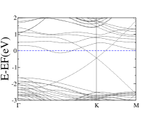
On Si-terminated surface, the Fermi level falls 0.4 eV above the Dirac point. The graphene like planes are n doped. This is confirmed by the opening of a gap in the case of 3 C layers (buffer +2). Tight binding calculations involving orbitals show that this is characteristic of a graphene bilayer where the two planes are not symmetric. In our ab initio calculation, the Fermi level falls above the highest unoccupied band minimum at K point. The comparison to tight binding calculations, shows that the two graphene layers are doped and that one plane is less doped than the other one. This is in agreement with recent ARPES and XPS measurements ohta ; rollings . For C terminated surfaces in the bulk truncated geometry, the Fermi level falls on the Dirac point and the graphene layers are neutral. On the other hand, the Fermi level of the C-deficient geometry (Fig. 4) is 0.4 eV above the Dirac point. It is fixed by states related to the 3 DB present in this structure. This stresses the role played by interface defects.
For the Si terminated surface the DB related state and the graphene derived states anticross indicating some interactions between them (inset of Fig. 3c). This is not the case for the bulk C terminated surface. This effect may have a crucial impact on transport properties of the film and explain the low electron mobilities of Si-face films compared to C-face films.x_ray
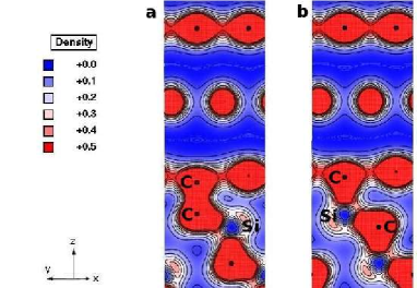
In Fig. 5, charge density contours show clear evidence of the existence of a covalent bond between the first graphitic C layer (buffer layer) and SiC. Charge density appears to be more delocalized in the subsequent graphitic planes as one can expect for graphene like layers.
In conclusion, we have shown that the first C layer on top of a SiC surface acts as a buffer layer and allows the next graphene layer to behave electronically like an isolated graphene sheet. The existence of strong covalent bonds to the first layer is in agreement with X-ray reflectivity data. The electronic structure of subsequent graphitic layers depends on the geometry of the interface and on the number of layers. Our calculations show clear evidence of a charge transfer from SiC to the graphene layers that depends on the interface geometry and results in a doping of these layers. We even show the possible opening of a gap at the Dirac point in agreement with ARPES results. Interface intrinsic defects induce states in the vicinity of the Fermi level. The interaction of these states with the graphene derived states depends on interface geometry and may explain the lower electronic mobility observed on Si-terminated surface. Because the defect density (i.e. DB states) is even larger for the actual cell, further experiments and calculations are needed to clarify the role of these states and their dependence on interface geometry and stacking order in these systems.
Acknowledgments
We thank P.Darancet, D. Mayou, V.Olevano, P.First, W.de Heer for fruitful discussions. This work is supported by: a computer grant at IDRIS-CNRS and the ACI CIMENT (phynum project); the National Science Foundation under Grant No. 0404084, by Intel Research and by the US Department of Energy (DE-FG02-02ER45956). The Advanced Photon Source is supported by the DOE Office of Basic Energy Sciences, contract W-31-109-Eng-38. The -CAT beam line is supported through Ames Lab, operated for the US DOE by Iowa State University under Contract No.W-7405-Eng-82. Any opinions, findings, and conclusions or recommendations expressed herein are those of the authors and do not necessarily reflect the views of the research sponsors.
References
- (1) C.Berger et al.,J.Phys. Chem.B 108, 19912 (2004)
- (2) C. Berger et al., Science 312, 1191 (2006)
- (3) K. S. Novoselov et al., Nature 438, 197 (2005)
- (4) Y. Zhang, Y.-W. Tan, H. L. Stormer,P. Kim, Nature 438, 201 (2005)
- (5) K. Nakada, M. Fujita, G. Dresselhaus, M. S. Dresselhaus, Phys. Rev. B 54, 17954 (1996)
- (6) K. Wakabayashi, M. Fujita, H. Ajiki, M. Sigrist, Phys. Rev. B 59, 8271 (1999)
- (7) I. Forbeaux, J. -M. Themlin, J. -M. Debever, Phys. Rev. B 58, 16396 (1998)
- (8) E.Rollings et al., J.Phys.Chem.Sol. 67, 2172 (2006)
- (9) M. L. Sadowski et al., Cond-mat/0605739
- (10) T. Ohta, A. Bostwick, T. Seyller, K. Horn, E. Rotenberg, Science 313, 951 (2006)
- (11) N.M.R. Peres, F. Guinea, A. H. Castro Neto, Phys. Rev. B 73, 125411 (2006)
- (12) G. Kresse and J. Hafner, Phys. Rev. B 47, 558 (1993)
- (13) J. P. Perdew and Y. Wang, Phys. Rev. B 33, 8800 (1986)
- (14) G. Kresse and J. Hafner, J.Phys. Condens. Matter 6, 8245 (1994)
- (15) A. Incze, A. Pasturel, P. Peyla, Phys.Rev.B 66, 172101 (2002); A.Incze PhD thesis (2002), Grenoble, France
- (16) The first C layer position is determined by the formation of strong covalent bonds with the substrate. This is well described by DFT. For subsequent C layers, we changed the interlayer spacing from 2 to 5 Å in the system made of 2 C layers on top of a Si terminated SiC surface. The change in total energy is lower than 0.5 eV. The E(d) (d is the C interlayer spacing) curve is similar to the curve calculated for graphite evc .
- (17) N. Mounet and N. Marzari, Phys. Rev. B 71, 205214 (2005)
- (18) J. Hass, R. Feng, T. Li, X. Li, Z. Zong, W.A. de Heer, P.N. First, E.H. Conrad, C.A. Jeffrey, and C. Berger, Appl. Phys. Lett. 89, 143106 (2006)
- (19) R. Feng, J. Hass, J. Millán, X. Li, M. Sprinkle, P.N. First C. Berger, and E.H. Conrad (to be published).
- (20) Y. Baskin and L. Mayer, Phys. Rev. 100 544, (1955)
- (21) R. E. Franklin, Acta Cryst. 4 253, (1951)
- (22) A. J. Van Bommel, J. E. Crombeen, and A. Van Tooren, Surf. Sci. 48, 463 (1975).
- (23) This can also be seen in a preliminary calculation by A. Mattausch and O. Pankratov published in the Proceedings of ECSCRM 2006.
- (24) S. Latil, L. Henrard, Phys. Rev. Lett. 97, 036803 (2006)
