Fabrication and Characterization of Electrostatic Quantum Dots in a Si/SiGe 2D Electron Gas, Including an Integrated Read-out Channel
Abstract
A new fabrication technique is used to produce quantum dots with read-out channels in silicon/silicon-germanium two-dimensional electron gases. The technique utilizes Schottky gates, placed on the sides of a shallow etched quantum dot, to control the electronic transport process. An adjacent quantum point contact gate is integrated to the side gates to define a read-out channel and thus allow for noninvasive detection of the electronic occupation of the quantum dot. Reproducible and stable Coulomb oscillations and the corresponding jumps in the read-out channel resistance are observed at low temperatures. The fabricated dot combined with the read-out channel represent a step towards the spin-based quantum bit in Si/SiGe heterostructures.
Individual spins in silicon/silicon-germanium (Si/SiGe) heterostructures have many desirable properties Vrijen2000 for solid-state implementations of spin-based quantum information processing. In silicon, electrons can have very long coherence times since they experience a very weak spin-orbit coupling and zero hyperfine interaction to nuclear spins in isotopically-purified structures Tyryshkin2003 . The tunable spin-orbital coupling and the ability to control the electron wave-functions allow the execution of electrically controlled g-factor tuning for logic operations Vrijen2000 .
Despite its potentials, the technologies for fabricating submicron devices in Si/SiGe two-dimensional electron gases (2DEGs) are not as established as those for GaAs/AlGaAs materials. One main technical difficulty is that the surface Schottky gates cannot be reliably made due to problems of Fermi level pinning and leakage paths to the 2DEG created by dislocations in strained materials. To overcome this difficulty, X. Z. Bo et al. Bo2002 and L. J. Klein et al. Klein2004 have recently fabricated quantum dots (QDs) by using atomic force microscope lithography on Si/SiGe heterostructures. In their devices, trenches are created by the lithography and the isolated 2D electron regions are used as gates to control a QD surrounded by the trenches.
Here we demonstrate a different fabrication technique to produce QDs in a modulation-doped Si/SiGe heterostructure. Our method has a better gate-QD coupling allowing for efficient electrostatic control of the QD. The QD can be potentially squeezed to hold only one electron or, in other words, a single spin, which is of particular interest for the purposes of quantum computation. Furthermore, a read-out channel can be fabricated adjacent to the dot for a noninvasive read-out of the spin state of the QD, similar to other GaAs/AlGaAs devices Elzerman2004 .
Molecular beam epitaxy (MBE) was used to grow the Si/SiGe heterostructure. The 2DEG resides in a 10 nm silicon channel 21.5 nm below the surface. Antimony (Sb) is incorporated into the donor layer via a delta-doping approach using an Sb4 source. The donor layer is separated from the silicon channel by a 5 nm Si0.7Ge0.3 spacer layer. A 10 nm Si0.7Ge0.3 layer and 6.5 nm Si cap were grown on the spacer layer. From the substrate to the Si channel, a step-graded SiGe/SiGeC buffer sequence and a 400 nm Si0.7Ge0.3 layer were grown. At room temperature, the mobility and concentration of the 2DEG are 1700 cm2/Vs and cm-2 respectively. At 4 K, these two quantities measure cm2/Vs and cm-2 respectively. Aluminum ohmic contacts to the 2DEG are established using rapid thermal annealing at for 2 min.
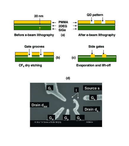
In our device, metallic side-gates are used similarly to that of the vertical QD in GaAs/AlGaAs heterostructures Austing1995 . The steps used to produce the Schottky gates are shown in Fig. 1. Electron beam lithography is used to pattern the QD structures on PMMA, Fig. 1(a). After developing, CF4 reactive ion etching is carried out to remove the 2D electron part of the device structure and to establish grooves for the side gates as shown in Fig. 1(b). The etching was very shallow reaching about 30 nm underneath the surface of the sample. This process is followed by evaporating a 10 nm/70 nm titanium/gold layer as indicated in Fig. 1(c), then the QDs (Fig. 1(d)) are obtained by metal lift-off in acetone. The etching process results in side-wall depletion, which insulates the metallic gates from the electron gas. Since titanium forms a Schottky barrier with the side SiGe wall, we expect relatively fewer dangling-bond-induced traps compared to that in unpassivated trenches Bo2002 ; Klein2004 . We have tested the leakage through the Schottky side gates to the 2DEG and found that most gates leak at positive gate voltages around 0.4 V or higher and at negative gate voltages around -3.0 V or lower.
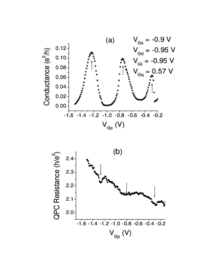
Now we shall demonstrate some of the characteristic features of the fabricated structures. Figure 2(a) shows Coulomb oscillations in the conductance of a quantum dot as a function of the plunge gate voltage at temperature K keeping other gate voltages at constant values. The conductance through the QD is measured using a standard lock-in technique with an ac voltage of a few hundred microvolts between the source and drain to avoid self-heating of the QD. In the figure, the number of electrons in the dot is decreased one-by-one when the magnitude of the voltage on the gate is increased. Devices with different sizes show a reproducible single electron charging effect and are stable over a few hours.
For quantum information processing, it is undesirable to measure the spin state by passing current through the dot. We have used a side quantum point contact (QPC) as an electrometer for noninvasive sensing of the number of electrons in QD, as this discrete electronic occupation can be used for projective spin-state read-out Elzerman2004 . In the tunneling regime, the resistance of the QPC channel is very sensitive to the potential variations caused by adding or expelling electrons from the QD Field1993 . Figure 2(b) shows that there are clear futures in the QPC channel resistance corresponding to the peaks in the Coulomb oscillations in Fig. 2(a). The spacing between two successive peaks is periodic and equals V for that particular quantum dot.
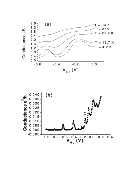
The evolution of the Coulomb oscillations for a small dot (geometrical diameter about 200 nm) at different temperatures is shown in Fig. 3(a). As the temperature increases, the oscillations broaden and they finally disappear at K. This rather large Coulomb charging energy is a result of the small QD size. Figure 3(b) shows the Coulomb oscillations for a larger dot (geometrical diameter about 350 nm) at 0.4 K. For the larger dot, the oscillations become visible at about K. Larger number of oscillations, and smaller are also seen, as expected.
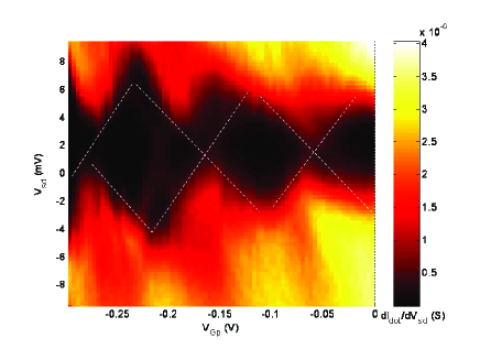
The single electron transport is also manifested in a so-called stability diagram that represents the differential conductance of the QD measured at different values of the source-drain voltages and the gate voltages on the plunge gate. A stability plot, obtained for the larger dot at 0.4 K with V ac excitation voltage applied between source and drain at 15 Hz, is shown in Fig. 4. The charging energy equals to and can be inferred from the figure by calculating the slope of the “diamonds” Klein2004 . The charging energy of 2 meV corresponds to a total capacitance of 80 aF. Representing the dot as a metallic disc with radius R, the total capacitance of the dot reads giving an effective diameter of about 190 nm for the QD. Here, is the permittivity of vacuum and is the dielectric constant of silicon.
In general, we are able to vary the number of electrons in the QDs one by one from 30-150 electrons. The number of electrons in the smallest dot with an effective diameter of about 75 nm still has a minimum of 30 electrons. This minimum number is limited by the maximum gate voltage which can be used without leakage. Currently, we are fabricating devices using another Si/SiGe heterostructure that has a much lower 2D electron concentration (about cm-2, a factor of 6 smaller than that of the current heterostructure) and a higher mobility of cm2/Vs. With these new devices, we expect to get into the few-electron regime, which becomes useful for quantum information applications.
In summary, a quantum dot with an integrated charge read-out channel has been fabricated using a 2DEG in a silicon/silicon-germanium heterostructure. The QD dot is laterally confined by metallic side-gates in etched grooves. The devices show a reproducible single electron charging effect that is stable over an extended period of time. The discrete electronic occupation of the quantum dots is effectively detected using the adjacent QPC electrometer. This device structure with improvement can be potentially used as a spin-based qubit. This work is supported by the Defense MicroElectronics Activity under grant number DMEA 90-02-2-0217 and MARCO MSD Center.
References
- (1) R. Vrijen, E. Yablonovitch, K. Wang, H. W. Jiang, A. Balandin, V. Roychowdhury, T. Mor, and D. DiVincenzo, Phys. Rev. A 62, 12306 (2000).
- (2) A. M. Tyryshkin, S. S. Lyon, A. V. Astashkin, and A. M. Raitsimiring, Phys. Rev. B 68, 193207 (2003).
- (3) Xiang-Zheng Bo, Leonid P. Rokhinson, Haizhou Yin, D. C. Tsui, and J. C. Sturm, Appl. Phys. Lett. 81, 3263 (2002).
- (4) L. J. Klein, K. A. Slinker, J. L. Truitt, S. Goswami, K. L. M. Lewis, S. N. Coppersmith, D. W. van der Weide, Mark Friesen, R. H. Blick, D. E. Savage, M. G. Lagally, Charlie Tahan, Robert Joynt, M. A. Eriksson, J. O. Chu, J. A. Ott, and P. M. Mooney , Appl. Phys. Lett. 84, 4047 (2004).
- (5) J. M. Elzerman, R. Hanson, L. H. Willems van Beveren, B. Witkamp, L. M. K. Vandersypen, and L. P. Kouwenhoven”, Nature, 430, 431, (2004).
- (6) D.G. Austing, T. Honda, S. Tarucha, Semicond. Sci. Technol. 11, 1995 (1995).
- (7) M. Field, C. G. Smith, M. Pepper, D. A. Ritchie, J. E. F. Forst, G. A. C. Jones, and D. G. Hasko, Phys. Rev. Lett. 70, 1311 (1993).