Photoluminescence rings in Corbino disk at quantizing magnetic fields
Abstract
Spatially resolved photoluminescence of modulation doped AlGaAs/GaAs heterojunction was investigated in a sample of Corbino disk geometry subject to strong perpendicular magnetic fields. Significant spatial modulation of the photoluminescence was observed in form of one or more concentric rings which travelled across the sample when the magnetic field strength was varied. A topology of the observed structure excludes the possibility of being a trace of an external current. The effect is attributed to formation of compressible and incompressible stripes in a 2DEG density gradient across the sample.
pacs:
PACS numbers: 73.43.Fj, 78.55.-mPhotoluminescence (PL) of AlGaAs/GaAs heterostructures contains information on a two-dimensional electron gas (2DEG) confined in the system. Various PL features have been identified typical for 2DEG in strong perpendicular magnetic fields. Kuk ; Turb ; Gold ; Couz ; Ray ; Zin ; Shi However, little attention has been paid to the spatial distribution of the PL. This is a relevant problem especially in the case of a 2DEG carrying an unballanced external current in magnetic fields, when a self-induced spatial inhomogeneity may be expected. A characteristic current dependent inhomogeneity of the PL has indeed been observed in recent experiments. Paas ; Nov01 ; Franken However, their interpretation is not straightforward: whereas in Refs. Paas, ; Franken, regions of bright PL along the sample edges have been attributed to a locally enhanced hole density, in Ref. Nov01, a non-radiative decay of excitons due to a vertical electric field field has been made responsible for observed stripes of quenched PL. In neither of the cases the PL structures could be directly and unquestionably associated with a current trace, in contrast e.g. to PL images of current filaments in a high-purity bulk GaAs.Eberle ; Hirsch
In a classical rectangular Hall bar sample it is difficult to distinguish, whether an observed inhomogeneity stems primarily from an inhomogeneous longitudinal current, or from a nonlinear transversal (Hall) potential. In a sample with rotational symmetry such a distinction should be possible merely by topological arguments: whereas the potential distribution preserves the symmetry of the edges, a trace of the current flow has to break this symmetry, since it connects the contacts of the sample. With the above idea in mind we investigated a spatial distribution of photoluminescence in a 2DEG sample with a Corbino disk geometry.
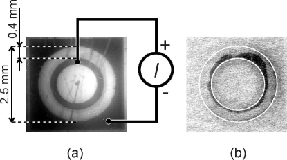
The investigated sample was cut from a modulation doped single heterostructure of grown by molecular beam epitaxy on a semiinsulating substrate. The heterostructure consisted of m GaAs buffer layer, 10 nm GaAlAs spacer layer, 100 nm GaAlAs source layer with nominal doping , and 20 nm GaAs cap layer. On a mm piece of the material two concentric ring contacts were patterned by annealing of Au/Ge/Ni. The contacts defined an annulus of 0.85 mm and 1.25 mm inner and outer radii, respectively. Inside the inner ring a free circular area has been left floating as a currentless reference.
The sample was mounted on an insulating carrier, and placed into a superconducting magnet inside of a liquid helium cryostat. The sample could be homogeneously illuminated by a set of red light emitting diodes; in all of the optical experiments we fed the diodes with a constant current of 1 mA, corresponding to an estimated power density of the incident light of 50 . The excited photoluminescence was photographed through an optical port by a CCD camera, with net resolution of about m. To pick out only the wavelengths of the near band gap luminescence, an interference filter with 820 nm central wavelength and 5 nm bandwidth was put into the optical path.
If cooled to 4.2 K while kept in dark, the sample showed pronounced Shubnikov–de Haas (SdH) oscillations. Using their period together with data on the low-field magnetoresistance we obtained and as density and mobility of the two-dimensional electrons, respectively. After illumination the density of the 2D electrons rose up to , accompanied be an increase in the apparent mobility to . It should be noted, however, that a strong parallel conductivity evolved at the same time, accompanied by a deformation of the SdH oscillations and by a strong reduction of their amplitude. This parasitic conductivity persisted up to temperature of about 115 K, indicating activated DX centers in the ternary layer.Moon
Figure 1 shows the basic result: when an external current is applied, a weak spatially inhomogeneous reduction of the PL intensity between the contacts occurs (Fig. 1a). The image of the quenched area can be highlighted by subtracting the constant PL background of the currentless sample at the same magnetic field. The difference image reveals a well defined dark structure in form of an irregular closed loop, which encircles the inner contact. When reversing the current the dark structure appears adjacent to the outer contact. As it will be discussed later, the particular shape, size and contrast of the quenched structure depend on the applied current and magnetic field; however, at all practical conditions the PL structure never appears to connect the two current contacts. Thus, a possible filamentation of the imposed current flow may immediately be excluded as a primary origin of the observed PL inhomogeneity.

The PL pattern is independent of the direction of the perpendicular magnetic field. On the other hand, it exhibits an oscillatory behavior when its strength is monotonously swept. At first, a dark ring structure arises adjacent to the positive contact; on increasing the dark structure departs from the contact and travels radially across the sample; with further increase in the structure arrives at the negative contact and disappears; a new dark ring arises at the positive contact when is further increased, and the scenario repeats for each period of SdH oscillations measured on the sample voltage.
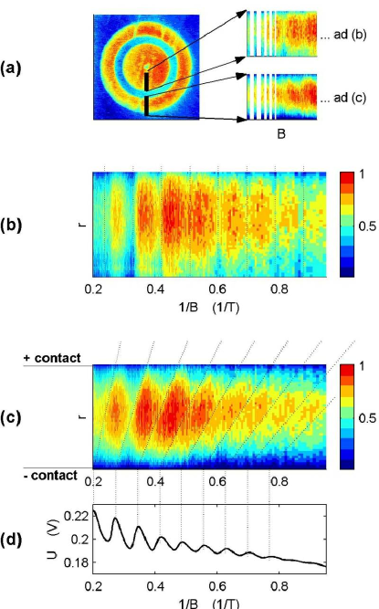
The PL rings emerge from a homogeneous PL background approximately simultaneously with the onset of electrically detectable SdH oscillations, similarly to the longitudinal quenched stripes in a Hall-bar geometry.Nov01 Bad signal-to-noise ratio, especially at low magnetic fields, and a weak contrast of the dark structures make it difficult to determine exactly their contours. However, a convincing impression of dark rings repeatedly travelling from one contact to another is obtained, if a series of static PL images taken at a slowly increasing magnetic field is joint together and looked at as a quickly running video sequence. To demonstrate this behavior in a single static figure we extracted a thin radial line out of each ”frame” of such a sequence, and stacked these line-profiles one after another in a streak image, with as abscissa, Fig. 2(a).

In the sample without current only vertical bursts of the PL intensity are seen in the streak image, Fig. 2(b), separated by darker grooves of reduced photoluminescence. The bursts occur simultaneously (though not uniformly) along the whole radial section, clearly demonstrating standing oscillations of the PL, which correspond to a periodic change in the occupation of the highest Landau level. If an external voltage is applied, the dark grooves in the streak image get tilted, Fig. 2(c), reflecting a motion of the dark rings in varying . When reversing the current bias, also the travelling direction (i.e. the tilting angle of the grooves in the streak image) reverses, pointing always from the positive to the negative contact in increasing .
Locations of the dark grooves in can well be approximated by straight lines, as indicated by a set of eye-guides in Fig. 2(b,c). This is in a clear contrast with a steep dependency of edge channel positions, theoretically treated by Ref. Chklo, and confirmed experimentally for low currents e.g. in Ref. AhlsCorb, . The travelling velocity of the PL rings (i.e. the tilting angle of the dark grooves in Fig. 2(c)) obviously changes from one SdH period to another, increasing with a decreasing filling factor. Accordingly, two or more rings can be observed simultaneously at low magnetic fields, whereas only one ring at a time exists at high .
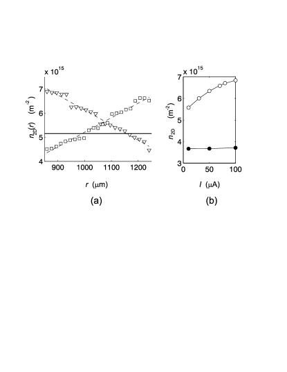
The -period of the PL ring occurrence (i.e. the dark grooves spacing) changes with the radius , as also seen from Fig. 2(c). On the other hand, at each radial coordinate the PL image period in is fairly constant in the whole range of . Thus, using this period dependence, a two-dimensional electron density can be extracted from the streak image Fig. 2(c) as a function of the radial coordinate. The result shown in Fig. 3(a) suggests that a significant gradient of the electron density exists in a sample with an externally imposed current. A slope of the gradient depends on the current magnitude, maximum is always at the negative contact.

Under a constant current bias the sample voltage exhibits well pronounced oscillations in varying . Their periodicity coincides with that of the dark PL ring recurrence at the negative contact, as seen in Figs. 2(c,d). Accordingly, also the voltage oscillation period varies with the current bias, reflecting a local filling factor near the negative contact. A current dependency of the electron density at the negative contact (i.e. the maximum ), acquired from the voltage period, is plotted in Fig. 3b. It should be stressed that no such dependence can be found in a sample prior to the first illumination, where the period of the voltage oscillations remains constant even for currents exceeding A.
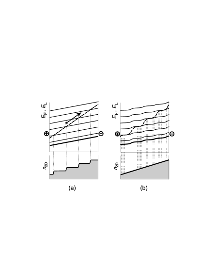
A qualitative explanation of the observed PL structures can be constructed starting from a one electron picture. Generally, in an electrically biased sample the slopes of both the Landau levels and the Fermi level have the same signs, given by the bias polarity. Furthermore, in a sample with a finite concentration gradient pointing from the positive to the negative contact the Fermi level crosses the Landau level system as schematically shown in Fig. 4(a). Upon increasing , the spacing of the Landau levels grows and the crossing points of the Landau levels and the Fermi level shift toward the negative contact. Let us note that this direction agrees with the sense of the observed PL ring motion and that this coincidence would not occur in case of an opposite concentration gradient.

In a more realistic approximation, the effect of Fermi level pinning has to be taken into account:Guven the electrons close to the Fermi surface tend to screen an external electric field and form compressible stripes of finite widths.Chklo Accordingly, instead of a set of lines, a set of compressible stripes of partially occupied Landau levels arises, separated by narrow incompressible regions of fully occupied or totally empty states, Fig. 4(b). The sense of the stripe motion in varying remains the same as in the one electron picture, i.e. the experimentally observed one.
A photoluminescence involving the 2D electrons depends on the magnetic field both with its wavelength and its intensity. However, the observed spatial structures in the PL images are to be attributed solely to changes in the intensity: except for a contrast, the same spatial structures have been obtained using interference filters of 820 and 830 nm central wavelengths. A plausible mechanism of the PL intensity variation can again be found within the qualitative picture according to Fig. 4(b): the PL intensity exhibits a maximum for electrons from the Fermi surface (Fermi edge singularity), i.e. from the compressible stripes in our case, whereas the PL is reduced in the incompressible ones.
A question remains on the origin of the gradient of the 2D electron concentration. In fact, for a Corbino sample geometry under external current an inhomogeneous 2DEG density has been predicted theoretically.Dyak ; Shik1 ; Shik2 There are, however, reasons for which we believe that those theories are not fully pertinent to our experiment. In particular, we have observed differences in the behavior of the sample prior to and after the illumination. For the most significant one we hold the above mentioned change in the electrically measurable SdH oscillations in the sample voltage: whereas there was no detectable current induced change in their period before the first illumination, a clear dependence has evolved between the period and the sample current after the illumination; let us recall that this dependence obviously correlates with the periodicity of the observed PL structures. Furthermore, a transition from a perfectly linear to a more complex and -dependent form of sample’s I-V curve has been found during the illumination.
As a more feasible explanation we regard a model which assumes a presence of some conducting (either contacted or floating) layer parallel to the 2DEG. The existence of such a parallel layer has been suggested by several authors and indirectly supported by various experimental results.Coldien ; Knot ; Jian ; Zheng ; Ebe ; Nov01 Possible origins include photogenerated holes accumulated at the buffer-substrate interface, DX-center induced conductivity in the ternary layer, and others. By solving an electrostatic problem corresponding to such a double-layer system, an electron density gradient can be shown to arise if a non-zero potential drop exists between the banks of the 2DEG layer.Coldien ; Shask1 A self-consistent solution of the electrostatics, Fermi statistics of 2D-electrons, and a realistic longitudinal conductivity function would then yield a quantitative correction to Fig. 4(b).
Conclusions. The PL pattern observed in a current biased sample at quantizing magnetic field has the form of one or more rings concentric with the contacts of the Corbino disk. This topology excludes the possibility of the PL pattern being a trace of a channel carrying an unballanced external current.
The PL rings have been found to travel periodically across the sample when sweeping the magnetic field. The rings travel the whole path from the positive to the negative contact in increasing magnetic field, with a velocity differing qualitatively from the one expected for the edge channels in a confining potential in a homogeneous sample.
Indications have been found that the sample behavior significantly differs before and after the first illumination. We suppose that the illumination—besides building up a parasitic conductivity—leads to a formation of a persistent equipotential layer parallel to the 2DEG. The existence of such a layer in a sample under current gives rise to an electron density gradient, confirmed experimentally by the varying periodicity of the observed photoluminescence pattern. Coming out from the non-zero density gradient a qualitative model has been formulated, which explains the observed PL structures in terms of compressible and incompressible stripes.
Acknowledgements.
The authors thank K. Výborný for valuable discussions, and Z. Výborný and V. Jurka for technical assistance. Support by the Humboldt foundation and the Deutsche Forschungsgemeinschaft is gratefully acknowledged by V.N. and W.P. The work was done in the framework of AV0Z1-010-914 program.References
- (1)
- (2) I.V. Kukushkin, K. von Klitzing, K. Ploog, Phys. Rev. B 37, 8509 (1988).
- (3) A.J. Turberfield, S.R. Haynes, P.A. Wright, R.A. Ford, R.G. Clark, J.F. Ryan, J.J. Harris, C.T. Foxon, Phys. Rev. Lett. 65, 637 (1990).
- (4) B.B. Goldberg, D. Heiman, A. Pinczuk, L. Pfeiffer, K. West, Phys. Rev. Lett. 65, 641 (1990).
- (5) N.N. Zinov’ev, A.V. Andrianov, L.J. Challis, C.T. Foxon, J.J. Harris, Surface Science 361/362, 392 (1996).
- (6) A.J. Shields, J.L. Osborne, M.Y. Simmons, D.A. Ritchie, M. Pepper, Semicond. Sci. Technol. 11, 890 (1996).
- (7) B. Couzinet, A. Raymond, M.I. Elmezouar, W. Zawadzki, M. Kubisa, B. Etienn, phys. stat. sol (b) 210, 635 (1998).
- (8) A. Raymond, M.I. Elmezouar, W. Zawadzki, M. Kubisa, B. Etienne, phys. stat. sol (b) 210 635 (1998)
- (9) A. Paassen, A. Zrenner, A.L. Efros, M. Stopa, J. Frankenberger, M. Bichler, W. Wegscheider, Phys. Rev. Lett. 83, 3033 (1999).
- (10) J. Frankenberger, A. Zrenner, M. Bichler, G. Abstreiter, Phys. Rev. B 65, 165307 (2002).
- (11) V. Novák, P. Svoboda, S. Kreuzer, W. Wegscheider, W. Prettl, Phys. Rev. B 64, 165302 (2001).
- (12) J. Hirschinger, F.-J. Niedernostheide, W. Prettl, V. Novák, Phys. Rev. 61, 1952 (2000).
- (13) W. Eberle, J. Hirschinger, U. Margull, W. Prettl, V. Novák, and H. Kostial, Appl. Phys. Lett. 68, 3329 (1996).
- (14) P.M. Mooney, T.N. Theis, Comments Cond. Mat. Phys. 16, 167 (1992)
- (15) D.B. Chklovskii, B.I. Shklovskii, L.I. Glazman, Phys. Rev. B 46, 4026 (1992).
- (16) E. Ahlswede, J. Weis, K. von Klitzing, K. Eberl, Physica E 12, 165 (2002).
- (17) K. Güven, R.R. Gerhardts, Phys. Rev. B 67, 115327 (2003).
- (18) V.B. Shikin, JETP Lett. 66, 581 (1997).
- (19) V.B. Shikin, JETP Lett. 69, 71 (1999).
- (20) M.I. Dyakonov, F.G. Pikus, Solid State Commun. 83, 413 (1992)
- (21) A.A. Shashkin, V.T. Dolgopolov, S.I. Dorozhkin, Sov. Phys. JETP 64, 1124 (1987).
- (22) G. Diener, J. Collazo, J. Phys. C: Solid State Phys. 21, 3305 (1988)
- (23) H.Z. Zheng, D.C. Tsui, and A. Chang, Phys. Rev. B 32, 5506 (1985).
- (24) G. Ebert, K. von Klitzing, G. Weimann, J. Phys. C 18, L257 (1985).
- (25) R. Knott, W. Dietsche, K. von Klitzing, K. Eberl, K. Ploog, Semicond. Sci. Technol. 10, 117 (1995).
- (26) P.H. Jiang, Y.J. Huang, W.K. Ge, D.Z. Sun, Y.P. Zeng, J. Appl. Phys. 64, 2488 (1988).