[
Towards the fabrication of phosphorus qubits for a silicon quantum computer
Abstract
The quest to build a quantum computer has been inspired by the
recognition of the formidable computational power such a device
could offer. In particular silicon-based proposals, using the
nuclear or electron spin of dopants as qubits, are attractive due
to the long spin relaxation times involved, their scalability,
and the ease of integration with existing silicon technology.
Fabrication of such devices however requires atomic scale
manipulation - an immense technological challenge. We demonstrate
that it is possible to fabricate an atomically-precise linear
array of single phosphorus bearing molecules on a silicon surface
with the required dimensions for the fabrication of a
silicon-based quantum computer. We also discuss strategies for the
encapsulation of these phosphorus atoms by subsequent silicon
crystal growth.
(To appear in Phys. Rev. B Rapid Comm.)
pacs:
03.67.Lx, 85.35.-p, 68.37.Ef, 68.43.-h]
A quantum bit (or qubit) is a two level quantum system that is the building block of a quantum computer. To date the most advanced realisations of a quantum computer are qubit ion trap [3] and nuclear magnetic resonance [4, 5, 6] systems. However scaling these systems to large numbers of qubits will be difficult [7], making solid-state architectures [8], with their promise of scalability, important. In 1998 Kane proposed a novel solid state quantum computer design [9] using phosphorus 31P nuclei (nuclear spin I = 1/2) as the qubits in isotopically-pure silicon 28Si (I = 0). The device architecture is shown in Fig. 1a, with phosphorus qubits embedded in silicon approximately 20 nm apart. This separation allows the donor electron wavefunctions to overlap, whilst an insulating barrier isolates them from the surface control A and J gates. These A and J gates control the hyperfine interaction between the nuclear and electron spins and the coupling between adjacent donor electrons respectively. For a detailed description of the computer operation refer to Kane [9]. An alternative strategy using the electron spins of the phosphorus donors as qubits has also been proposed [10].
One of the major challenges of this design is to reliably fabricate an atomically-precise array of phosphorus nuclei in silicon - a feat that has yet to be achieved in a semiconductor system. Whilst a scanning tunnelling microscope (STM) tip has been used for atomic scale arrangement of metal atoms on metal surfaces [11], rearrangement of individual atoms in a semiconductor system is not straightforward due to the strong covalent bonds involved. As a result, we have employed a hydrogen resist strategy outlined in Fig. 1b. Here the array is fabricated using a resist technology, much like in conventional lithography, where the resist is a layer of hydrogen atoms that terminate the silicon surface. An STM tip is used to selectively desorb individual hydrogen atoms, exposing the underlying silicon surface in the required array. STM induced hydrogen desorption has been developed and refined over the past ten years [12] and has been proposed [13] for the assembly of atomically-ordered device structures. We demonstrate a process to adsorb single phosphine molecules in a predefined array, with atomic resolution, which we have developed specifically for the fabrication of a silicon quantum computer. The incorporation of these arrays in silicon is then discussed.
Whilst hydrogen lithography at the tens of Angstrom linewidth scale has been used to selectively expose the silicon surface to oxygen [14], ammonia [14], iron [15], aluminium [16], gallium [17] and cobalt [18], there has only been one recent report of adsorption, at the atomic scale, in this case individual and clusters of silver atoms [19]. Here we demonstrate the controlled adsorption of a linear array of single phosphine molecules in the extreme case of single hydrogen atom desorption sites for direct application to the fabrication of a scalable silicon quantum computer. This technical achievement has answered the critical questions of whether a hydrogen resist is effective during exposure to phosphine and whether or not phosphine will adsorb to an STM-exposed site sufficiently small to achieve one and only one PH3 molecule at that site.
The requirements for this quantum computer design are very stringent. In order to undertake high resolution lithography the silicon surface must be atomically flat with a low defect density to allow the formation of a near perfect resist layer, where one hydrogen atom bonds to each surface silicon atom. The ability to then desorb individual hydrogen atoms requires a sharp, large cone angle tungsten tip in order to form 1 nm desorption sites. These sites are subsequently exposed to high purity phosphine gas for the required phosphorus atom placement (Fig. 1b). We demonstrate each of these steps below. Throughout this process particular attention must be made to avoid the introduction of any spin or charge impurities that would be fatal to the operation of the quantum computer [9].
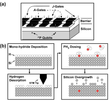
The final fabrication step outlined in Fig. 1b which is not the subject of this paper, but presents a significant challenge, is to encapsulate the phosphorus qubits in a crystalline lattice of isotopically-pure silicon-28 [20]. The main difficultly in this step is to ensure the phosphorus atoms incorporate into the silicon crystal and remain in their ordered atomic array. The most direct route to achieving this is to desorb the hydrogen resist from the surface by heating to 700 K followed by epitaxial silicon growth over the phosphorus array. A possible concern with heating the surface is the potential to induce lateral surface diffusion of the phosphorus atoms in the array. However it is known that the phosphorus atom in the PH2 molecule, with a single bond to the silicon, incorporates into the silicon surface with a more stable threefold coordination geometry over the lower temperature range of 550-650 K [21]. We can avoid heating the surface at all during hydrogen desorption by either direct optical excitation at = 157 nm [22] or electron bombardment [23]. An alternative room temperature approach that will help to incorporate the phosphorus into the silicon lattice without significant diffusion involves photo-induced excitation of the attached PH2 molecule to increase its chemical activity with the surface [23]. Finally it is also possible to leave the hydrogen resist and grow epitaxial silicon directly on the mono-hydride surface [24]. In all above cases 10-30 Å of epitaxial silicon can be grown at low temperatures, down to room temperature [25] to encapsulate the phosphorus, followed by elevated temperature growth at 500 K to maintain crystallinity [25]. We will return to the issue of phosphorus incorporation in our final discussion.
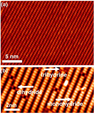
The first step in fabricating a phosphorus qubit array is to prepare a clean, defect free silicon surface. Fig. 2a demonstrates an optimally-prepared Si(001)21 surface consisting of rows of -bonded silicon-silicon dimers. By heating the surface to 1200 ∘C in a variable-temperature ultra-high vacuum STM system and performing a controlled cool-down [26] we have achieved large defect free regions. The “bean” shaped protrusions in this filled state image correspond to the charge overlap of the electrons in the dangling bonds on each silicon surface atom giving rise to a weak -bond. These dangling bonds make the surface reactive, allowing the subsequent adsorption of species such as hydrogen and phosphine.
The adsorption of atomic hydrogen on the Si(001)21 surface can occur in three ways depending on the surface temperature, forming either a mono-, di- or tri-hydride [27]. An atomic hydrogen source consisting of a heated tungsten filament and water-cooled heat shroud has been used for this work. Fig. 2b shows an image taken at room temperature of a low defect density Si(001)21 surface after exposure to high purity atomic hydrogen at 600 K. It can clearly be seen that a near uniform coverage of the mono-hydride phase has occurred, where one hydrogen atom bonds to each silicon atom. Sites of di-hydride, where two hydrogen atoms bond to each silicon, and tri-hydride, a mixture of the other two phases, are also indicated. We have found that all three phases passivate the surface and act as an effective resist during subsequent exposure to phosphine. Comparison of current-voltage spectroscopy before and after hydrogen dosing (not shown) confirms the existence of a hydrogen passivated surface, with the silicon *-antibonding peak evolving into the silicon-hydrogen antibonding peak after hydrogenation [28].
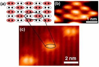
An STM tip is then used to desorb hydrogen from the surface by application of a controlled voltage pulse between the tip and sample [12]. Optimisation of the geometry of an oxide-free tungsten tip and controlled voltage pulses (sample bias 6 V and tunnelling current 1 nA for 1 ms) makes atomic resolution desorption possible. In order to allow the adsorption of one phosphine molecule, and therefore only one phosphorus atom, it is necessary to desorb an area that exposes less than or equal to two silicon dimers as shown schematically in Fig. 3a. This is because phosphine bonds to the Si(001)21 surface with a c(42) surface periodicity as demonstrated in Fig. 3b where we have dosed a clean Si(001)21 surface with phosphine [21]. The STM image in Fig. 3c shows three 1 nm diameter hydrogen desorption sites in a row with a pitch of 4 nm on a hydrogen terminated Si(001)21 surface. This image, with such a close spacing between sites, highlights the atomic resolution desorption achieved. The distance between sites can easily be increased to the required qubit spacing of 20 nm, and we have performed controlled lithography of single desorption sites in a line 100 nm in length. The desorption sites in Fig. 3c appear as bright protrusions as a result of the extension of electron density out of the surface due to the silicon dimer surface states of the exposed silicon dangling bonds [12]. Fig. 3 demonstrates that these desorption sites are sufficiently small to allow only one phosphine molecule to bond to the surface at each site.
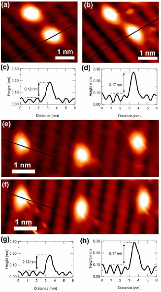
Following STM lithography to expose small regions of the Si(001)21 surface it is then necessary to adsorb the individual phosphorus atoms or qubits using phosphine gas. Figs. 4a and 4b show atomic resolution images of two hydrogen desorption sites 1.5 nm apart on a dimer row both before and after exposure to phosphine gas. The effectiveness of the hydrogen resist as a barrier to phosphine adsorption is demonstrated by the uniform hydrogen coverage after phosphine dosing except at the previously desorbed hydrogen sites. In order to observe any changes after phosphine exposure we have specifically created single hydrogen desorption sites, rather than larger desorption sites (as in Fig. 3) and present high resolution images where the spacing between sites is very small. Here the bright protrusion at each of the desorption sites in Fig. 4a is the signature of the single silicon dangling bond, after desorption of just one hydrogen atom, in this case from the left side of the dimer. The remaining hydrogen on the silicon dimer is known to be transient [29] and we have observed it diffusing from one side of the dimer to the other.
In order to obtain high purity phosphine gas delivery, the PH3 micro-dosing system and its connection to the UHV STM employed internally electro-polished gas lines assembled in a clean-room environment. Mass spectra taken in the chamber during the exposure at a pressure of 10-8 mbar reveal no significant increase in the partial pressure of any other species. The sticking coefficient of phosphine on the clean silicon surface is 1 [21]. Fig. 4b shows the same area as Fig. 4a after exposure to phosphine gas at room temperature. Analysis of the line profiles in Fig. 4c and 4d shows a characteristic increase of 0.05 nm in the height of the protrusion after phosphine dosing [30]. Figs. 4d and 4e show three desorption sites, in a line perpendicular to the dimer rows, before and after phosphine dosing. The associated line profiles (Figs. 4f and 4g) again show a 0.05 nm height increase. This increase, observed at all adsorption sites over several images, was calibrated against an atomic step edge on the same surface (not shown) both before and after phosphine dosing. This reproducible increase confirms the adsorption of a PH3 molecule and corresponds to the difference between the exposed silicon dangling bond and the adsorbed phosphine. The transient nature of the hydrogen atom on the silicon dimer can account for the asymmetry of the image in Fig. 4b where one phosphine molecule has bonded to the left silicon in the dimer (upper) and another phosphine molecule has bonded to the right silicon in the dimer (lower).
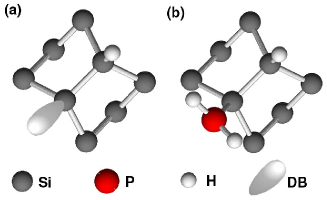
Studies of the interaction of phosphine with the clean Si(001)21 surface [21] suggest that PH3 molecularly adsorbs to one end of a silicon dimer and can then dissociate to PH2 provided enough silicon dangling bonds are available nearby for the re-adsorption of the dissociated hydrogen. The absence of available dangling bond sites on the hydrogen-terminated surface inhibits this dissociation step. Fig. 5a shows a schematic of a single dangling bond site on a hydrogen terminated surface before phosphine dosing and Fig. 5b shows the proposed structure of Si-PH2 after dissociation of the adsorbed PH3. In this configuration the adsorbed phosphorus atom maintains the tetrahedral geometry and threefold coordination, with the PH2 bonded to one end of the dimer [21]. A similar dissociative process and Si-XH2 configuration is understood to occur in the adsorption of NH3 [31] and AsH3 [32] on the Si(001)21 surface, where both nitrogen and arsenic are isoelectronic with phosphorus.
In the above discussion we have demonstrated the process of controlled single phosphine molecule adsorption for the extreme case of single hydrogen atom desorption sites. In future work it will be important to maintain the ordered atomic array during the final silicon growth step (final panel of Fig. 1b). Here the optimisation of the size and crystallographic orientation of the desorption sites will be critical. Dissociation of singly-bonded PH2 to threefold coordinate P + 2H can proceed above 500 K [25], provided there are suitable dangling bond sites that overcome competition with the recombinative desorption of PH3. An alternative option is to dose the hydrogen-patterned surface with phosphine gas at elevated temperatures (550 K) to directly induce phosphorus incorporation into the first atomic layer. We have independently performed elevated temperature studies which indicate that at these temperatures, the silicon surface is stable.
We have demonstrated the effectiveness of a hydrogen resist as a barrier to phosphine adsorption and used STM lithography for the controlled placement of single phosphorus bearing molecules on a silicon surface - central to the construction of a silicon based quantum computer. This process, shown for closely spaced controlled doping, demonstrates the achievability of more widely-spaced (20 nm), precisely positioned phosphorus qubit arrays over large areas. Whilst it is not yet possible to guarantee the subsequent overgrowth steps required for the Kane architecture, this letter demonstrates a significant advance in the solid-state qubit fabrication process and bodes well for the realisation of a scalable silicon quantum computer. Finally, it is important to note that the fabrication strategy demonstrated here is also directly applicable to other silicon based quantum computer architectures [10].
We would like to thank I. Andrienko, T. Kamins, G. J. Milburn, S. Prawer, C. Thirstrup and S. Williams for useful discussions. This work is funded by the Australian Research Council Special Research Centre scheme, the Australian Government, the US National Security Agency, and the US Advanced Research and Development Activity.
REFERENCES
- [1] e-mail: job@phys.unsw.edu.au
- [2] present address: School of Mathematical and Physical Sciences, University of Newcastle, Callaghan, New South Wales, 2308, Australia
- [3] C. A. Sackett, et al., Nature 404, 256 (2000).
- [4] I. L. Chuang, L. M. K. Vandersypen, Xinlan Zhou, D. W. Leung, S. Lloyd, Nature 393, 143 (1998).
- [5] I. L. Chuang, N. Gershenfeld, M. Kubinec, Phys. Rev. Lett. 80, 3408 (1998).
- [6] J. A. Jones, M. Mosca, Phys. Rev. Lett. 83, 1050 (1999).
- [7] W. S. Warren, Science 277, 1688 (1997).
- [8] D. Loss, D. P. DiVincenzo, Phys. Rev. A 57, 120 (1998).
- [9] B. E. Kane, Nature 393, 133 (1998).
- [10] R. Vrijen, et al., Phys. Rev. A 62, 012306 (2000).
- [11] M. F. Crommie, C. P. Lutz, D. M. Eigler, Science 262, 218 (1993).
- [12] C. Thirstrup, M. Sakurai, T. Nakayama, M. Aono, Surf. Sci., 411, 203 (1998) and references therein.
- [13] J. R. Tucker, T. -C. Shen, Solid State Electronics 42, 1061 (1998).
- [14] J. W. Lyding, G. C. Abeln, T. -C. Shen, C. Wang, J. R. Tucker, J. Vac. Sci. Technol. B 12, 3735 (1994).
- [15] D. P. Adams, T. M. Mayer, B. S. Swartzentruber, J. Vac. Sci. Technol. B 14, 1642 (1996).
- [16] T. -C. Shen, C. Wang, J. R. Tucker, Phys. Rev. Lett. 78, 1271 (1997).
- [17] T. Hashizume, S. Heike, M. I. Lutwyche, S. Watanabe, Y. Wada, Surf. Sci. 386, 161 (1997).
- [18] G. Palasantzas, B. Ilge, J. De Nijs, L. J. Geerligs, J. Appl. Phys. 185, 1907 (1999).
- [19] M. Sakurai, C. Thirstrup, M. Aono, Phys. Rev. B. 62, 16167 (2000).
- [20] H. Bracht, E. E. Haller, R. Clark-Phelps, Phys. Rev. Lett. 81, 393 (1998)
- [21] D. S. Lin, T. S. Ku, R. P. Chen, Phys. Rev. B 61, 2799 (2000) and references therein.
- [22] T. Vondrak, X. -Y. Zhu, Phys. Rev. Lett. 82, 1967 (1999).
- [23] H. Guo, P. Saalfrank, T. Seideman, Prog. Surf. Sci. 62, 239 (1999)
- [24] M. Copel, R. M. Tromp, Phys. Rev. Lett. 72, 1236 (1994)
- [25] D. J. Eaglesham, H. -J. Gossmann, M. Cerullo, Phys. Rev. Lett. 65, 1227 (1990).
- [26] B. S. Swartzentruber, Y. W. Mo, M. B. Webb, M. G. Lagally, J. Vac. Sci. Tech. A 7, 2901 (1989).
- [27] K. Oura, V. G. Lifshits, A. A. Saranin, A. V. Zotov, M. Katayama, Surf. Sci. Rep. 35, 1 (1999).
- [28] R. J. Hamers, Ph. Avouris, F. Bozso, Phys. Rev. Lett. 59, 2071 (1987).
- [29] E. Hill, B. Freelon, E. Ganz, Phys. Rev. B 60, 15896 (1999).
- [30] A slightly larger height in the line profile of the dimer rows is observed after PH3 dosing. Such a difference can frequently occur due to minor changes in imaging conditions between scans, which results in the STM tip extending further into the gap between dimer rows. However the height difference due to PH3 adsorption is measured from the top of the dimer rows to the top of the protrusion and is not therefore affected by this.
- [31] Zhi-Heng Loh, H. C. Kang, J. Chem. Phys. 112, 2444 (2000) and references therin.
- [32] J. E. Northrup Phys. Rev. B 51, 2218 (1995).