Development of Large area Gamma-ray Camera with GSO(Ce) Scintillator Arrays and PSPMTs
Abstract
We have developed a position-sensitive scintillation camera with a large area absorber for use as an advanced Compton gamma-ray camera. At first we tested GSO(Ce) crystals. We compared light output from the GSO(Ce) crystals under various conditions: the method of surface polishing, the concentration of Ce, and co-doping Zr. As a result, we chose the GSO(Ce) crystals doped with only 0.5 mol% Ce, and its surface polished by chemical etching as the scintillator of our camera. We also made a 1616 cm2 scintillation camera which consisted of 9 position-sensitive PMTs (PSPMTs Hamamatsu flat-panel H8500 ), the each of which had 88 anodes with a pitch of 6 mm and coupled to 88 arrays of pixelated 6613 mm3 GSO(Ce) scintillators. For the readout system of the 576 anodes of the PMTs, we used chained resistors to reduce the number of readout channels down to 48 to reduce power consumption. The camera has a position resolution of less than 6mm and a typical energy resolution of 10.5% (FWHM) at 662 keV at each pixel in a large area of 1616 cm2.
Furthermore we constructed a 1616 array of 3313 mm3 pixelated GSO(Ce) scintillators, and glued it to a PMT H8500. This camera had the position resolution of less than 3mm, over an area of 55 cm2, except for some of the edge pixels; the energy resolution was typically 13% (FWHM) at 662 keV.
, , , , , , , , , , , and
1 Introduction
We have developed an advanced Compton camera for gamma-ray astronomy in the range of 100 keV to 20 MeV [1]. It needs a scintillation camera as a detector for Compton-scattered gamma rays with a good energy and position resolution and a large area because the resolution and the efficiency for the scattered gamma rays contribute to the angular resolution and the efficiency of the advanced Compton camera. In addition, radiation hardness and a high counting-rate performance of the scintillation camera are required. For these reasons, we chose a GSO(Ce) (Gd2SiO5:Ce) crystal as a scintillator, and the PSPMT H8500 (Flat Panel PMT produced by Hamamatsu[2]) as a position-sensitive photon device.
GSO(Ce) has advantages in astronomical use, such as having a higher-Z, faster decay time than NaI(Tl), a higher light output than BGO, greater radiation hardness and less radioactivation than most other known scintillators. Furthermore, GSO(Ce) can be easily cut and polished, since it is nonhydroscopic.
The PSPMT H8500 was recently developed as a promising device for nuclear physics and medicine, for example, PET and SPECT [3] [4] [5] [6]. It has 88 anodes with a 6 mm pitch and 12-stage metal channel dynodes. The advantage of this PMT is that it has a much smaller dead space and a larger effective area than that of the previous multi-anode PMTs. The effective area of this PMT is 4949 mm2, which is 89% of the package size.
In this paper we report on the results of measurements with pixelated GSO(Ce) scintillators and the performance (energy resolution and position resolution) of the scintillation camera developed by us.
2 Measurements of Pixelated GSO(Ce) Scintillators
There are different aspects that characterize the performance of a pixelated GSO(Ce) scintillator. One is the pixel size. The width of 6 mm and the thickness of 13 mm were chosen for our scintillation camera in order to fit the pitch of the anodes of PSPMTs, and the radiation length. One of the other important issues is the method of surface polishing. There are two established methods of polishing: one is chemical etching, and the other is mechanical polishing. It was reported that there was little difference between the performances of pixelated scintillators polished with these methods [7]. However, mechanical polishing is more expensive than chemical etching. Another important issue is the concentration of Ce as a scintillation activity impurity, and additional dopants. The light-decay time becomes faster as the concentration of Ce increases, although increasing the concentration of Ce decreases the optical transmittance of the crystal. It was also reported that doping at 200 ppm of Zr to GSO(Ce) improves the optical transmittance of the crystal [8].
We measured the light outputs from several crystals under different conditions of polishing or doping impurity in order to examine how important these are. There were 8 types of pixelated scintillators, which differed in the concentration of Ce, the presence of Zr and the ingot. We enveloped each pixel scintillator by a reflector (Goatex) and coupled the crystal face with an area of 66 mm2 or 46 mm2 to a single anode PMT (R6231 Hamamatsu) using optical grease (OKEN 6262). We then irradiated it with 662 keV gamma rays from a 137Cs source through a 3 mm collimator. Figure 1 shows the relative light outputs and energy resolution at 662 keV. The systematic errors were due to limits in the reproducibility of gluing the reflector to the crystal. It shows that the method of polishing and the optical transmittance caused by the concentration of Ce are not more important for the performance of our pixel size of 6613 mm3 than the difference of the ingot. However, there is a significant difference between only 1 mol% Ce doped crystals with a size of 4620 mm3 and the others. This shows a significant decreasing of the optical transmittance caused by Ce and the improvement of transmittance caused by doping Zr for longer crystal with a thickness of 20 mm.
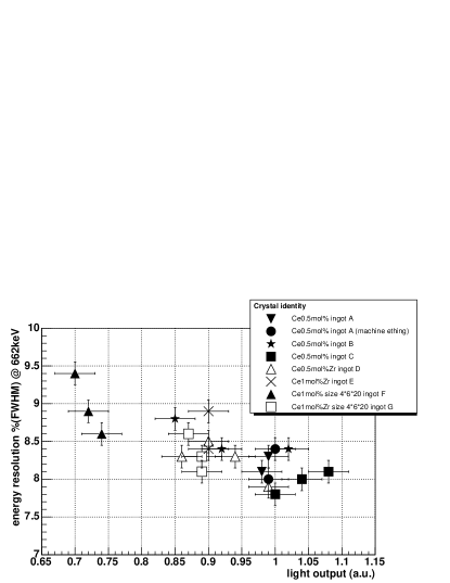
Based on the above studies, we chose crystals that were polished by chemical-etching and doped with only 0.5 mol% Ce for our camera. We made an 88 array of pixelated GSO(Ce) scintillators. Each pixel was optically separated by Vikuiti 3M ESR, which is a multilayer polymer mirror with a thickness of 65 m and a reflectance of 98%. The construction of this array is described in reference [6].
3 Performance of a 55 cm2 scintillation camera and a 1616 cm2 scintillation camera
We made a 55 cm2 scintillation camera by coupling an 88 GSO(Ce) array to a PMT H8500 using optical grease. In order to limit power consumption, the readout circuit of the camera consisted of 8 resistive chains, 16 ch amplifiers, and ADCs, as described in reference [9].
The image of each pixel scintillator was clearly resolved by a flood field of irradiation of 662 keV gamma ray, which means that the position resolution was less than the pixel pitch of 6 mm. We also obtained the energy spectrum of each pixel with energy resolution of 10% (FWHM) @ 662 keV.
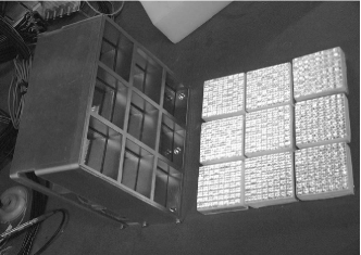
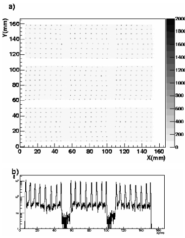
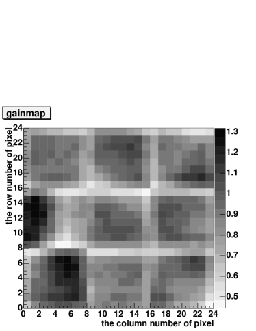
This 55 cm2 camera can be easily extended to a larger camera. We constructed a 1616 cm2 camera with 33 PMTs, as shown in Fig. 2. The pitch of PMTs was 53 mm and the effective area of the camera is 82%. The number of readout channels of the camera was only 48 channels with 24 resistive chains. All 576 pixels were clearly resolved by a flood field of radiation of 662 keV gamma rays, as shown in Fig. 3 (a) and (b), which show an event map and an x-projection map at the 12th row (78 mmy84 mm), respectively. The events located between each pixels seem to be multi-pixel hits events by Compton-scattered gamma rays or accidental events. The energy resolution (FWHM) was 31.0% at 122 keV, 18.2% @356 keV, 13.9% @511 keV, 10.7% @662 keV, 9.6% @835 keV, 8.6% @1173 keV for the typical pixel, 9.8%@662 keV(FWHM) for good pixels and 13%@662 keV(FWHM) for bad pixels. Figure 4 shows a map of the relative light output of each pixel. It mainly shows differences among anode gains of the PMTs. However the light output was too low at some edges of each PMT. This was probably due to a misalignment of the array of crystals to the PMTs. The measurable energy ranges of this camera are 80-1300 keV and 100-900 keV, for good and bad pixels, respectively.
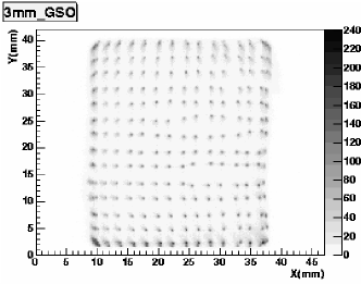
In order to improve the position resolution, we tried to use smaller pixels with a width of 3mm compared to that of the anode pitch of H8500. Such developments were already reported on earlier [3] [4] [5]. We made a 1616 array of pixelated 3313 mm3 GSO(Ce) scintillators and coupled it to the H8500. In the flood field of irradiation of 662 keV gamma rays, the pixel image was clearly separated, except for some of edge pixels, as shown in Fig. 5. However the energy resolution deteriorated to 12% @662 keV compared to that of scintillation cameras with 6613mm3 pixels.
4 Summary
We measured the light outputs from GSO(Ce) scintillators under different conditions, and chose a non-Zr doped, chemical etched GSO(Ce) crystal with a size of 6613 mm3 for our scintillation camera. We constructed 88 arrays of the crystal, and developed a 1616 cm2 GSO scintillation camera. The performance of this camera is sufficient to be used as a Compton-scattered gamma-ray camera for our advanced Compton camera. We constructed an advanced Compton camera and tested its performance.
References
- [1] A.Takada et al., Nucl. Inst. and Meth. A 546 (2005) 258.
- [2] Hamamatsu technical data sheet H8500-H8500B, Feb 2005, printed in Japan, http://www.hamamatsu.com
- [3] R.Pani et al., Nucl. Inst. and Meth A 527 (2004) 54; Nucl. Inst. and Meth A 513 (2003) 36.
- [4] M.Gimenez et al., Nucl. Inst. and Meth. A525 (2004) 298.
- [5] D.Herbert et al., Nucl. Inst. and Meth. A518 (2004)399.
- [6] N.Inadama et al., IEEE Trans. Nucl. Sci., 51, 1, 58 (2004); IEEE Trans. Nucl. Sci., 52, 1, 15, (2005);
- [7] K.Kurashige et al., IEEE Trans. Nucl. Sci., 45, 3, 522 (1998).
- [8] Hitachi chemical technical report No.44 13 (2005-1), Printed in Japan, http://www.hitachi-chem.co.jp/japanese/report/;
- [9] H.Sekiya et al., Proceedings for IWORID7 (2005); appear in Nucl. Inst. and Meth A.