Further author information: (Send correspondence to I.J.)
I.J.: E-mail: jung@physics.wustl.edu, Telephone: 1 314 935 6254
Test of Thick Pixelated Orbotech Detectors with and without Steering Grids
Abstract
We report here on the optimization of 0.5 cm thick pixelated Orbotech CZT detectors with regards to the best contacting materials and the use of steering grids. We evaluated the performance of different contacting materials. Our study differs from earlier ones in that we investigated the performance of different anode and cathode materials separately. We obtain the best performance with Au cathodes. For different anode materials Ti and In give the best energy resolutions. The detector (2.02.00.5 cm3, 88 pixels) shows excellent 59 keV, 122 keV and 662 keV energy resolutions of 1.4 keV, 1.9 keV, and 7.4 keV, respectively. Furthermore, we report on using steering grids to improve on the performance of the pixelated detectors. Previously, the benefit of steering grids had been limited by additional electronic noise associated with currents between the negatively biased steering grids and the anode pixels. We are currently exploring the possibility to isolate the steering grid from the CZT substrates by a thin layer of Al2O3. We performed a series of measurements to determine by how much the isolation layer reduces the grid-pixel currents. Comparing the currents between two Au contacts before and after isolating one of the two contacts from the CZT with a 700 nm thick layer of Al2O3, we measure that the isolation layer reduces the currents by a factor of about 10 at 500 V. We present some results from a detector before and after deposition of an isolated steering grid. The grid indeed improves on the detectors energy resolution and detection efficiency. We show that simulations can be used to model the anode to cathode charge correlation in excellent agreement with the experimental results.
keywords:
CZT, X-ray and Gamma-ray detectors, contact technology, steering grid1 INTRODUCTION
Cadmium Zinc Telluride (CZT) has emerged as the detector material of choice for the detection of hard X-rays and soft gamma-rays with excellent position and energy resolution and without the need for cryogenic cooling. We report here on tests with CZT substrates from the company Orbotech Inc. [1] (formerly Imarad). They are grown with a Modified Horizontal Bridgeman (MHB) process. The MHB process results in a high yield of good crystals and in very uniform substrates.
The bulk resistivity ( ohm cm) is lower than that of the more conventionally grown High-Pressure Bridgman CZT. Using high-workfunction cathode materials that form blocking Shottky contacts on the -type CZT substrates, the bias currents can be reduced by more than one order of magnitude so that the associated shot noise no longer deteriorate the energy resolution [2, 3, 4]. Different cathode materials have been studied extensively. In this contribution, we give a brief report on results obtained with different anode materials. A full description of this study will be given elsewhere (Jung et al., in preparation).
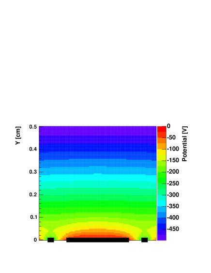
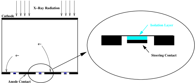
Most current CZT detectors use “electron-only” detection strategies [5, 6] to ameliorate the problems associated with the poor hole mobilities and short hole trapping times in CZT (cm). One can use for example the “small pixel effect” [5, 6] so that charge generated inside the detector induces pixel currents only briefly before impinging on the anode pixels. The anode signals become largely independent of the location of the charge generation and the “depth of interaction” (DOI). An additional DOI correction can be used to further improve the energy resolution. The DOI can be estimated from measuring the drift time of the electrons [7, 8] and from measuring the anode to cathode charge ratio [9]. Some groups (see e.g. [8]) use steering grids to improve the performance of pixelated detectors. Steering grids ameliorate the energy resolutions and detection efficiencies of pixelated detectors by steering electrons away from the areas between pixels towards the pixels [10]. Furthermore, steering grids modify the weighting potential of the pixels. The result is a stronger small pixel effect and an additional enhancement of the energy resolution of the detectors. Most groups bias the steering grids at voltages of between -30 and -60 V relative to the anode pixels. Owing to the limited surface resistivity of CZT, large grid-pixel currents start to flow for higher grid bias voltages. However, simulations show that a grid bias between -100 V and -300 V is required to appreciably modify the electric field inside the detectors (see Fig. 1). We are thus exploring the possibility to isolate the grids from the CZT substrates (Fig. 2). The isolation layer can reduce the grid-pixel currents while allowing the electric field to enter the detector. The second main topic of this contribution are studies of the effectiveness of Al2O3 isolation layers. Furthermore, we present some results from a detector before and after deposition of an isolated steering grid, and compare experimentally measured data with simulations.
2 Detector Fabrication
We use Orbotech CZT substrates, 2.02.00.5 cm3, contacted with a planar cathode and 88 anode pixels with a pitch of 0.25 cm and a pixel width of 0.16 cm. We polish the CZT substrates with Al suspension, and etch them in 5% Br-95% Methanol solution. After etching for 1.5 minutes, the substrates are rinsed in various Br-Methanol solutions with decreasing Br concentration. The contacts are deposited with an electron beam evaporator. We use masks and standard photolithographic techniques to deposit the pixels and/or the steering grids.
2.1 Test Electronics
The CZT detectors are temporarily mounted with gold-plated, spring-loaded “pogo-pin” contacts. To measure the cathode-pixel and pixel-pixel IV curves a set-up consisting of a PC, a programmable Bertan high voltage power supply, a programmable AD switch, and a Keithley electrometer is used.
The energy resolution is determined mostly for flood-illuminating the detectors with X-rays. A hybrid electronic readout is used. The pulse shape is read out for four channels: the central anode pixels and the cathode. These pixels are AC coupled and amplified by a fast Amptek 250 amplifier followed by a second amplifier stage. After digitizing the amplified signals using a 500 MHz oscilloscope they are sent via an Ethernet connection to a PC. With this setup the electron drift-time can be determined with an accuracy of 10 ns. Sixteen additional channels can be read out with an ASIC to measure the pulse height information. The ASIC gives amplified and shaped signals which we digitize with a custom designed VME board. The FWHM noise of both readout chains lies between 5 keV and 10 keV.
We have made a few measurements using collimated X-rays. A 7.5 cm thick tungsten collimator is used with a tapered hole. The hole diameter is 0.02 cm at the source and 0.05 cm at the detector end of the collimator. The CZT cathode is situated 0.10 cm off the collimator. The collimator position is controlled by a x-y stage with 1m accuracy. Eight channels can be read out, the information obtained is the pulse height of the signals. The FWHM noise of anode channels lies between 5.75 keV to 8.1 keV for cathode biases between V and V and grid bias between V and V. The FWHM noise of the cathode channel lies between 7.2 keV and 41 keV. More information on this experimental setup as well as previous results can be found in [7].
We measure the detector performance at different temperatures by placing the detector and the readout electronics inside a Tenney climate chamber and cooling or heating the set-up to the desired temperature.
3 CZT detectors contacted with various metals
We have performed a detailed study of various contact metals by optimizing the cathode and anode contacts separately. In our earlier study [4] we used Orbotech detectors contacted with In cathode and anodes. Replacing the In cathodes with Au, Cr, Ni, Pt and Ti cathodes, we observed a reduction of the cathode-pixel currents by factors of ten and higher. Whereas detectors with Au, Cr, In and Ti cathodes gave very similar 662 keV energy resolutions, Ni and Pt gave substantially poorer performance. In another study, we used identical materials for the cathode and anode contacts. Of Au, Cr, In and Pt, it was Au that gave the best result, followed in order of performance by Pt, In and Cr. In this study, we had used individual CZT crystals several times. This procedure eliminates uncertainties associated with a variable crystal quality that plague studies that use several crystals. However, we observed that the performance of some crystals deteriorated with time, owing to the wear and tear from polishing off the contacts and depositing new contacts.
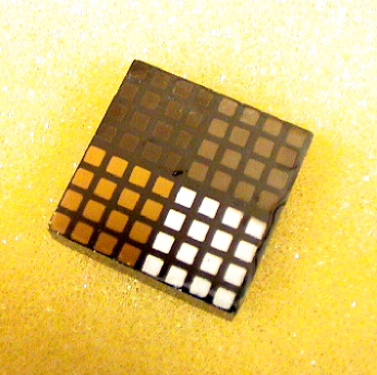
Here, we use a slightly different strategy, depositing four metals on four quadrants of one detector. The procedure has the advantage that the processing procedure is identical for all four metals. It has the disadvantage that the crystal quality might vary across the crystal. We plan to exclude the latter possibility by evaporating a single metal on the anode and test for spatial variations of the crystal quality. Based on the previous results we used
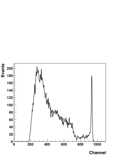
Au as cathode material, and compared four different anode materials Au, Cr, In, and Ti (see Fig. 3). We measured the performance for the central 16 pixels, i.e. four pixels of each material. We analyzed each pixel carefully and did a detailed analyses of the detection efficiency on the depth of interaction (DOI). One Ti pixel showed a drastic efficiency drop for a region in the middle of the detector and was excluded from the analyses. We obtain the best energy resolutions for the Ti and In pixels with little variation between those two metals. For a Ti pixel we obtain 59 keV, 122 keV and 662 keV energy resolutions of 1.4 keV (4.0 keV), 1.9 keV (4.2 keV), and 7.4 keV (9.6 keV), respectively (values in brackets are before subtraction of amplifier noise). Fig. 4 shows the 662 keV energy spectrum.
4 Oxidation layer
The voltage that can be applied to a steering grid is limited by the current between the grid and the anode contacts. To overcome this problem, we explored the possibility to isolate contacts from the CZT substrate by a high-resistivity layer. The idea is to use this technique for the steering grid, see Fig. 2. As isolation material we chose Al2O3 because of its high resistivity (cm ) and excellent mechanical properties.
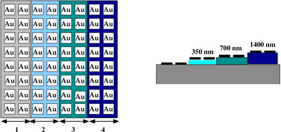
In order to examine the effect of oxidation layers we deposited gold contacts on Al2O3 layers of different thicknesses (0 nm, 350 nm, 700 nm, 1400 nm) on a CZT substrate (see Fig. 5). We then measured the current between adjacent contacts as function of the applied bias. The thickest Al2O3 layer (1400 nm) partially peeled off and contacts were deposited on top of the Al2O3 and as well as directly on the CZT. For these contacts we did not measure IV curves.
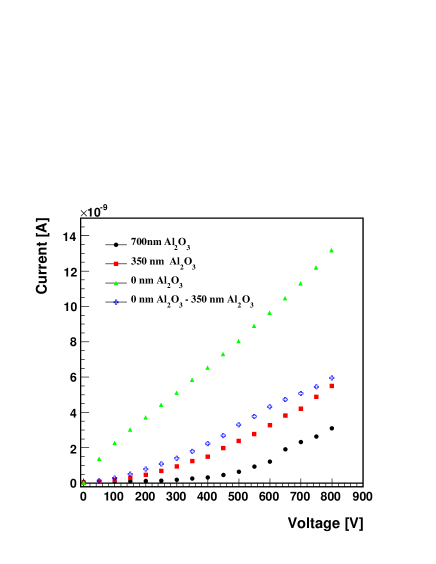
Fig. 6 shows the IV curves between different contacts. It can be recognized that the Al2O3 layers do indeed reduce the currents between adjacent contacts, even if one of the contacts is not isolated. In the latter case, the IV curve is not symmetrical and the current depends on the sign of the applied voltage. We only give the dependency for the contact with 0 nm Al2O3 at ground and negative voltages applied to the contact with 350 nm Al2O3. One can clearly see, that the thicker the isolating layer, the smaller the current at constant voltage.
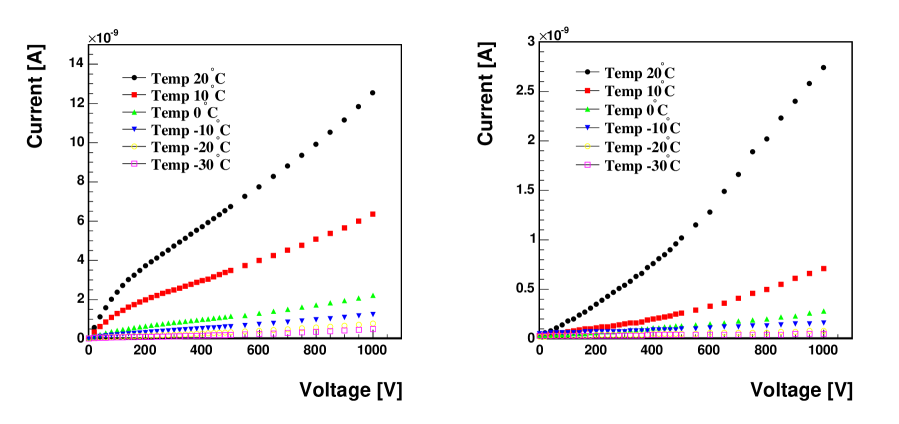
In satellite experiments like the proposed Energetic X-ray Imaging Survey Telescope (EXIST) satellite [13], CZT detectors would be used at minus-Centigrade temperatures. We thus measured the contact-contact IV curves for temperatures between -30∘ and +20∘ in 10∘ steps for two contacts deposited directly on the CZT and for two contacts deposited on top of 700 nm Al2O3. Fig. 7 shows the results. The currents decrease as the temperature decreases from 20∘ to -30∘: at 800 V bias, from 9.9 nA to 0.36 nA without isolation layer and from 2 nA to 0.04 nA with isolation layer. Thus, lowering the temperature from 20∘ to -30∘ reduces the bias current by more than one order of magnitude even without any isolation layer, but by two orders of magnitude with the 700 nm Al2O3 layer.
5 Performance of a CZT detector with and without an isolated steering grid
We tested an Orbotech CZT detector (2 x 2 x 0.5 cm3) contacted with an In cathode and In pixels before and after depositing an isolated steering grid. We used here a 150 nm thick Al2O3 layer. Although the results from the previous section show that the isolation layer should be thicker, we obtained encouraging results even with the thin isolation layer. The detector is shown in Fig. 8.
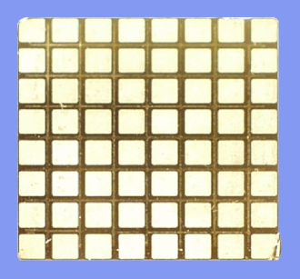
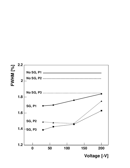
Figure 9 shows the energy resolutions of the three central pixels for flood-illumination with 662 keV photons. Without a steering grid, the three pixels achieved energy resolutions of 2.10%, 2.03% and 1.85%. With steering grid biased at -30 V, the performance of the same three pixels improved to 1.69%, 1.49% and 1.39%, respectively. The energy resolutions changed little for steering grid voltages between 0 V and -200 V. Below -200 V, the performance deteriorates. We conclude (see section 4) that the isolation was still too thin, as the grid-pixel current deteriorated the energy resolution. A detailed analysis of data taken with a collimated X-ray beam shows that the grid improves the detection efficiency for events between pixels. The number of good events increases by a factor of 3 for events in the gap between pixels.
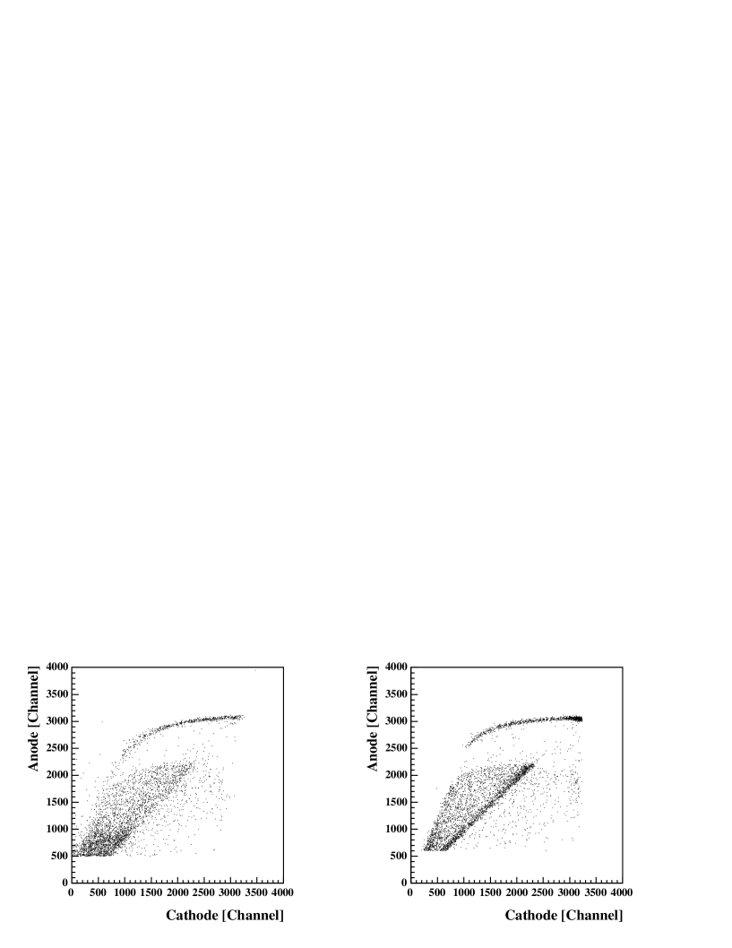
At the end of this contribution, we want to show that detector simulations can be used to model the data from the CZT detector with astonishing success. We use the Geant 4 code for simulating the photon interactions, a 3-D Poisson solver developed by S. Komarov, and an in-house developed code for tracking electrons and holes through the detector. Figure 10 shows the anode signal as a function of the cathode signal for experimentally measured and simulated data (662 keV flood illumination). The detector was radiated by a collimated 137Cs source. We get an excellent agreement when using an electron mobility of cm2 /V/s, electron lifetime of s, a hole mobility of cm2 /V/s and a hole lifetime of s. The electron mobility is consistent with an estimate based on the applied voltage and the measured electron drift times.
6 Summary and Conclusions
In this report, we present the results from several activities to optimize Orbotech CZT detectors. We tested detectors with standard In anode contacts and different cathode contacts. All the cathode contacts reduced the leakage current by more than one order of magnitude compared to the original In cathode. Au, Cr, In and Ti cathodes gave very similar 662 keV energy resolutions. On a different CZT detector, we replaced both, anode and the cathode contacts with identical material. In this study, Au gave the best results, followed in order of performance by Pt, In, and Cr. We tested four different anode materials. Ti and In gave excellent almost identical results. For further improvements one can use steering grids. Our results show that one can use an 700 nm thick Al2O3 isolation layer beneath the steering grid to reduce the current between grid and pixel. A first detector with isolated steering grid shows a significant improvement in energy resolution and detection efficiency. We plan to test other isolation materials and to continue to optimize the use of Al2O3. One can use isolation layers also for other CZT detectors designs such as Frish-grid and cross-strip detectors.
Acknowledgements.
We are grateful to S. Komarov for sharing his Poisson solver with us. We thank Orbotech Inc. for their cooperation. We acknowledge L. Sobotka, D. Leopold, and J. Buckley for helpful discussions. Thanks to electrical engineer P. Dowkontt, and electrical technician G. Simburger for their support. This work is supported by NASA under contracts NNG04WC176 and NNG04GD70G, and the NSF/HRD grant no. 0420516 (CREST).References
- [1] Orbotech Inc., Rabin Park, 10 Plaut Street, Rehovot, Israel
- [2] Vadawale, S. V. et al., Proc. of SPIE 5540, p. 22-32, 2004
- [3] Krawczynski, H., Jung, I., Perkings, J., Burger, A., Groza, M. Proc. of SPIE 592202-1, 2005
- [4] Jung, I., Groza, M., Perkins, J., Krawczynski, H., Burger, A. Proc. of SPIE 592202-1, 2005
- [5] Barret, H. H., Eskin, J. D. 1995, Phys. Rev. Lett., 75, 156
- [6] Luke, P.N. 1995, In: Procs. Of the ”9th International Workshop on Room Temperature Semiconductor X- and Gamma-Ray Detectors, Associated Electronics and Applications”, Grenoble, France, 18-22 Sept., 1995
- [7] Kalemci, E., Matteson, J., Nucl. Instr. Methods in Phys Research Section A, 2002, 478: p. 527-537
- [8] Zhang, F., He, Z. Proceedings SPIE, p. 135-143, 5540, 2004
- [9] Krawczynski, H., Jung, I., Perkins, J., Burger, A., Groza, A. Proceedings SPIE, p. 49, 5540, 2004
- [10] Bolotnikov, A., Nucl. Instr. Methods in Phys Research Section A, 1999, 432: p. 326-331
- [11] Shipley Company, LLC, 455 Forest Street, Marlborough, MA 01752, USA
- [12] S. Agostinelli et al., Geant4–a simulation toolkit, NIM A506, 250-303,2003
- [13] Grindlay, J. E. & the EXIST Team 2005, New Astron. Rev., 49, 435, 2005
- [14] Jung, I. Astroparticle Physics, in press