Characterizing Charge Diffusion in CCDs with X-rays
Abstract
We demonstrate the effectiveness of two techniques for using x-rays to evaluate the amount of charge diffusion in charge coupled devices (CCDs). We quantify the degree of charge diffusion with two parameters: , the standard deviation for a Gaussian diffusion model, and Q, a ratio of the point spread function (PSF) peak to its wings. and Q are determined by fitting a model to a pixel energy histogram, and by summing the PSF of all x-ray events, respectively. Using seven test devices, we investigate the precision of these two techniques and demonstrate that they produce compatible results. The histogram fitting method is sensitive to the structure of the electric field within these devices, in addition to the inherent charge diffusion properties. The Q ratio is a very simple parameter to measure and provides an easily accessible method for quickly evaluating a CCD’s diffusion length.
1 Introduction
The use of Charge Coupled Devices (CCDs) as light collectors for photometry and spectroscopy is ubiquitous in modern observational astronomy. To understand fully the limits and capabilities of these devices it is extremely important to have a set of standard methods for testing and quantifying their properties. There are a number of useful CCD characteristics that are relatively straightforward to measure. For example, carefully refined techniques for testing the gain, linearity, and charge transfer efficiency (CTE) have been developed (Janesick, 2001). One important CCD trait for which an efficient and practical testing procedure does not exist is charge diffusion.
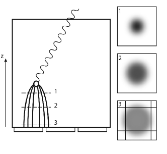
Figure 1 depicts schematically the process of charge creation and collection within a CCD. When a photon reaches the surface of a CCD it penetrates through some depth of silicon before it is absorbed. At the point of interaction this photon liberates one or more charge carriers. A photon with energy less than 4 eV creates one charge carrier. Higher energy x-rays produce a packet of charge in which the number of charge carriers is proportional to the energy of the photon. These charge carriers are either electrons or holes, depending on the CCD design. Hereafter we will assume that the buried channel is in an n-type semiconductor, so the charge carriers are electrons. The electron thermal velocities cause them to wander away from their original location into neighboring pixels. This spreading effect is what is termed charge diffusion. The electrons produced by photon absorption are eventually converted into a digital image, so charge diffusion places a fundamental physical limit on the resolution in the final image produced by a CCD.
Kraft et al. (1995) characterized charge diffusion in the process of evaluating quantum efficiency in x-ray CCDs, but their method involved a synchrotron source to produce a continuum of x-ray energies. Janesick (2001) also describes several techniques, such as measuring the modulation transfer function by projecting a sinusoidal light pattern across the CCD. In general, these methods can be effective, but they require either expensive specialized equipment or a significant investment of time. Such procedures are better suited to CCD manufacturers or engineering labs. Despite the demonstrated importance of understanding charge diffusion effects when designing astronomical instruments, there is currently no method for effectively evaluating charge diffusion that is accessible to the astronomical community without specialized equipment.
The techniques presented here rely on the use of soft x-rays from a mild radioactive source as a means of producing discrete, single photon events. These events are approximately point sources, since the size of the initial charge cloud is generally very small compared to the size of the pixels (Tsunemi et al., 1999). Of course, the experimenter has no control over where the x-rays land on the CCD surface or at what depth in the silicon each photon produces charge, so the x-ray events are randomly distributed throughout the volume of the CCD. Thus, we can gain little information by fitting a model to an individual event. An x-ray interacting near the surface of a low-diffusion device will spread charge over a large area, much like an x-ray interacting deeper down but in a device with higher charge diffusion. We can, however, break this degeneracy by modeling the entire ensemble of x-ray events and including the absorption probability as a function of depth (i.e. absorption probability increases exponentially with depth, so there will be far more interactions deep in the silicon than near the surface). For the two methods described here, we compare the histogram of pixel energies or the stacked and summed x-ray PSF to models that incorporate all of the available information about the charge collection process.
In the following section we describe the experimental setup and data collection procedures, as well as the formula for the calculation of the Q ratio. §3 details the creation and interpretation of K- pixel histograms, while §4 explains the theoretical model used to fit those histograms. We present results for the two methods in §5 and final conclusions in §6.
2 Experimental Setup and Procedures
Seven devices, labeled A-G, were used for the diffusion measurements. The first three are CCID-20 chips, chosen primarily because of their disposability - these CCDs were not likely to be used in a science-grade instrument, so damages incurred while testing them would not have been disastrous. The other four are CCID-45 Orthogonal Transfer Array (OTA) devices (Tonry et al., 1997). Each OTA has 64 individually addressable cells of approximately 500x500 pixels each. Table 1 lists the relevant information for all of the devices used. This set of seven CCDs provides a useful variety of physical parameters that affect the measured charge diffusion, such as silicon thickness and pixel size. The OTAs have the unique additional feature of allowing the voltage level of the substrate to be adjusted during testing, which provides another way to modify the diffusion properties while holding all other parameters constant.
| Device | Model | Thick. | Pix. Size | **From histogram fits. See section 4 | Resistivity | Notes |
|---|---|---|---|---|---|---|
| (CCD-) | (CCID-) | |||||
| A | 20 | 20 | 15 | 4 | 0.3 | bright defects; useable area 85% |
| B | 20 | 45 | 15 | 6 | 5 | bad parallel CTE along one side; |
| useable area 90% | ||||||
| C | 20 | 45 | 15 | 8 | 5 | tree-ring pattern fab. error |
| D | 45 | 45 | 10 | 10 | 5 | variable substrate voltage |
| E | 45 | 45 | 12 | 10 | 5 | variable substrate voltage |
| F | 45 | 45 | 12 | 12 | 14 | variable substrate voltage |
| G | 45 | 75 | 12 | 14 | 14 | variable substrate voltage |
To provide soft x-ray illumination, we use a 1 mCi Fe55 x-ray source. The Fe55 isotope emits x-rays when the nucleus captures an inner electron and becomes manganese. The most important x-ray emissions are the Mn K- event at 5.899 keV and the K- line at 6.490 keV. K- and K- x-rays interact in the silicon and produce a characteristic charge cloud equivalent to 1620 and 1778 electrons, respectively. Each of the four devices is mounted in a dewar that has a beryllium window in its faceplate, opaque to optical and infrared light but transparent to x-rays. By placing the Fe55 x-ray source directly against this window while the CCD is integrating, we get a dark image with hundreds of isolated single x-ray events.
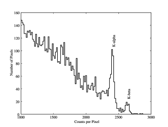
Figure 2 shows a simple histogram of all pixel values from an x-ray image of CCD-A. This histogram includes every pixel in the image (above a threshold of 1000 ADU), regardless of whether it is identified as a K- pixel or not. Such histograms are useful for accurately measuring the gain of a device, but to measure charge diffusion we really want to limit ourselves to those pixels in the immediate vicinity of an x-ray event. To produce the required x-ray pixel histogram, an x-ray image is scanned with a point source locating algorithm, which locates all pixels that are adjacent to a K- x-ray event. This algorithm first creates a raw histogram, such as the one in Figure 2, and locates the K- peak to determine , the number of ADUs that corresponds to a complete K- charge cloud (i.e. 1620 electrons times the gain of the device). We then examine all pixels that have a signal more than seven times the RMS noise of the background, along with their eight immediately adjacent pixels. For each patch of nine pixels, we subtract a constant background level and calculate the sum of nine pixel values, . If this sum is close to , meaning
then all nine pixels are tagged as ’K- pixels’ and are included in the calculation of Q and in the x-ray pixel histogram.
To measure Q, the 3x3 arrays of K- pixels, centered on the brightest pixel, are stacked and summed to produce a composite x-ray PSF. Q is then defined as the normalized ratio of the sum of the eight outer pixel values to the peak pixel value in the composite PSF:
| (1) |
Thus, for a device with zero charge diffusion so that all 1620 electrons produced by a K- x-ray are collected in a single pixel every time the Q ratio is zero. For infinite charge diffusion so that each of the nine pixels receives an equal fraction of the total charge Q is unity.
3 The X-ray Pixel Histograms
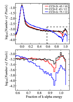
After computing Q, the algorithm then collects the complete set of all K- pixels (meaning all nine pixels from every patch centered on a K- event) and bins them into a histogram indicating what fraction of the x-ray’s energy was deposited in each pixel. To facilitate comparison with other devices and models, these x-ray pixel histograms are normalized such that the integral over all histogram bins is unity. These histograms are dominated by the background pixels, clustered around zero energy, so we display them on a log scale to highlight the subtle features near unity, which are strongly affected by the amount of charge diffusion. Figure 3 shows three x-ray histograms, demonstrating how physical properties of the CCD alter the histogram appearance.
The prominent features of these x-ray histograms can be explained in terms of the physical process of charge diffusion and collection. The strong peak around an energy value of zero is of course due to the pixels included in each 3x3 patch that have very little or no contribution from the nearby K- electrons. This peak extends into negative energy values because of noise fluctuations that leave some pixels below the median background level. To the right of this peak, as should be expected, the slope of the histogram is mildly negative through the intermediate energy bins. The first feature of interest to the determination of charge diffusion is the slope discontinuity, which is particularly prominent in CCD-G as shown in Figure 3.111We emphasize here that these histograms are plotted on a logarithmic scale, so these are in fact very subtle slope discontinuities. This slope discontinuity indicates a sudden decrease in the number of pixels containing a large fraction of the K- electrons. The energy at which this critical point occurs marks the energy remaining in the central pixel when an x-ray lands at the center of a pixel and the surface of a CCD. In any CCD, there are essentially two ways for an x-ray event to deposit a large fraction of its charge in a single pixel: it can land very near the center of the pixel’s square cross-section (allowing it lots of room to spread out within a single pixel), or it can interact with the silicon at a vertical height close to the gates (giving it very little time to spread out to other pixels). In CCDs with small pixels (such as CCD-D in Fig. 3) the first avenue is less effective, so the discontinuity point is translated to the left relative to large-pixel devices. In thick devices, the second effect is suppressed because the x-rays must travel through a greater volume of silicon to reach the requisite depths for containing the charge cloud in one pixel. Thus, thicker devices (such as CCD-G in Fig. 3), have fewer single pixels holding most of the K- electrons.
The final peak of these x-ray histograms is populated by single-pixel x-ray events. These are events in which the entire charge cloud is collected in one pixel. The presence of this peak in all of our x-ray histograms indicates that there is a sizeable probability for an x-ray penetrating deep into the CCD to deposit all of its energy into one pixel, rather than to spread a small fraction of it to neighboring pixels. As explained in §4, this trait is amplified by the presence of pixel barrier fields, which effectively focus charge clouds into pixel wells.
4 The Diffusion Model
To construct a model for comparison with the histograms described above, we consider an x-ray incident on the backside of a CCD that is absorbed at some height z above the frontside gate, as shown in Figure 1. The potential difference across the device from the backside to the buried channel produces an electric field that draws the electrons into the potential well which defines each pixel. If these were free electrons in empty space, they would be accelerated by this electric field. Inside a silicon lattice, however, these charges are impeded by collisions with lattice atoms and it can be shown that the drift velocity is proportional to the electric field at that height: . (Janesick, 2001, p.478) As the electrons are gradually pulled downward, they also execute a random walk horizontally, so that when they are finally collected in the gate structure the result is a substantially more extended profile than the original charge cloud. This final charge distribution is generally taken to be a Gaussian (Hopkinson, 1987; Janesick, 2001), although some calculations have shown that it should be more centrally peaked (Pavlov & Nousek, 1999; McCarthy et al., 1995). For simplicity, we restrict ourselves to the classic Gaussian charge distribution in all models.
We can take the RMS horizontal displacement to be proportional to the square root of the time it takes to reach the frontside gate at z=0:
| (2) |
In the simplest case, we can take the electric field to be constant with depth, so that a device with thickness d and potential difference V from frontside to backside has and we can now write
| (3) |
where is the standard deviation of the Gaussian diffusion cloud that would result from an x-ray interacting at the surface, where z = d. Now for a given value of and a K- x-ray event at a known height z we can create a final Gaussian distribution of charge. If we also choose an (x,y) position for the center of the cloud relative to the pixel boundary, we can integrate that final charge distribution over a 3x3 array of CCD pixel boundaries. To create a histogram from these pixel values, we want to repeat this process for a large number of x-ray events spread over an appropriate range of (x,y,z) values. For this, we need to know what fraction of x-ray events is likely to occur at any given depth in the silicon. K- photons in silicon have an e-folding absorption depth of 27.8 , so in a device of thickness d the fraction of absorption events occuring between height and from the bottom is:
| (4) |
The last physical effect that we must consider is the presence of barrier fields produced by the gate structure on the frontside of each device. The division of any CCD into pixels necessarily requires potential barriers which delineate the individual pixel wells. These barriers introduce a transverse electric field that prevents electrons very deep in the silicon from crossing over into neighboring pixels. We simulate this effect by introducing a barrier field height parameter, , such that once an electron reaches a height it can no longer diffuse away from its current position. This effectively truncates the diffusion process at a height above the buried channel. To accommodate this, we rewrite Eq. 3 as:
| (5) |
Thus, in our models, a 75 thick device with a barrier field height of 11 exhibits similar diffusion characteristics to a 65 thick device with a 1 barrier field. The one important difference is that the final 11 of the first device will absorb substantially more x-rays than the final 1 of the second device, meaning that there will be more single-pixel x-ray events populating the final peak of the x-ray histogram. Hence, the effect of increasing in our models is to amplify the final histogram peak at the expense of the energy bins just below the peak.
To produce a model energy histogram, we divide the silicon thickness into thin slabs. For each slab, Eq. 5 determines the apparent (z) at that depth, and Eq. 4 sets the relative number of events that have that (z). Next, we create a regular grid of (x,y) values arranged across one triangular eighth of the surface of a single pixel. Due to the symmetry of a square pixel, this is effectively the same as using a grid that extends across the entire pixel surface. For each (x,y) pair, we use the appropriate to the current slab to create a final Gaussian diffusion cloud projected onto the pixel grid. We then integrate over each pixel to determine the total x-ray counts detected for each event, and collect these pixel values into a normalized histogram in exactly the way that was done for the actual data. The final result is an x-ray histogram model with a known that can be directly compared to the real histogram.
To fit a model to each device we repeat this process for a wide range of and . The silicon thickness and intrinsic noise are fixed parameters for each device. From the resulting library of model histograms, we choose the curve that most closely matches the data histogram and record that model’s value of as our measured . Figure 4 shows an actual histogram for CCD-G along with the three closest matches from our model histogram library. The range in for these three models is 4% of the pixel width, or 0.48 for this 12 device. From these model histogram fits we can determine that the precision of is . All three models use a barrier field height of 14 , which is 19% of the total 75 thickness, and is close to the pixel width. In general, all of the best fitting models for a given device agree to within 1 on the height of the barrier field, regardless of the substrate voltage.
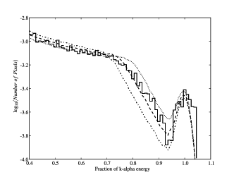
The measured barrier field heights for these seven devices are of the order of the size of the pixels. As a general rule, changing the barrier field height in our model has no effect on the position of the slope discontinuity point, which is the primary indicator of . The height of the final peak and the depth of the preceding trough in each histogram are the sole indicators of . In devices with very low charge diffusion, such as the 20 thick CCD-A, our determination of is less precise, because x-ray events have to be very close to the pixel boundaries for the barrier field to have any effect due to the inherently small size of the diffusion cloud. These low-diffusion devices will also yield somewhat less accurate measures of . When there is very little charge diffusion the slope discontinuity point that indicates the value of is very close to the final peak in the histogram, and can therefore be confused by the presence of the preceding trough feature. Table 1 lists the barrier field heights measured from histogram fitting in column 5.
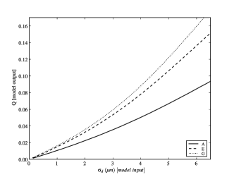
For the Q measurements, we simply need to translate our measured Q ratio into a physical measurement that can be directly compared to the value in microns. For this purpose we employ the same setup to produce a model aggregate PSF, and perform the sum and division of the nine pixels to get a value of Q. For each device the three physical properties of thickness, pixel size, and barrier field height are used as parameters for the model to define a curve that shows the input value of plotted against the output Q. Figure 5 shows these curves for three of the seven devices tested. From this plot we can take our unitless measured Q value and translate it directly into a value of in .
5 Results
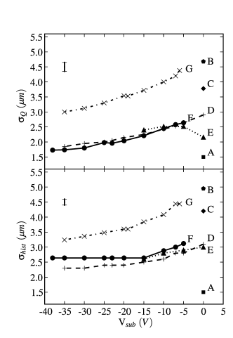
Using the procedures described above, we determine a value of from histogram fitting, and a value of from the summed PSF for each device (and at multiple substrate voltages in the case of the OTAs). These results are shown in Figure 6. The upper panel of Figure 6 plots the values determined from histogram fitting against the substrate voltage for all seven devices. The three non-OTA devices (CCD-A, B and C), are plotted as single points at = 0. The lower panel of Figure 6 provides the same plots for as a function of substrate voltage.
From these plots we can discern a number of important effects. First, our two methods both verify that thickness has a strong affect on a device’s charge diffusion. The 75 thick CCD-G has almost a factor of two more charge diffusion than the 45 OTA devices D, E, and F. CCD-A, at a thickness of 20 has more than a factor of two less diffusion than the 45 CCD-B and C. Secondly, the distinct histogram shapes resulting from differences in pixel size that are shown in Figure 3 produce the same physical diffusion length when we take into account the pixel size in our translation to in . Thus, the curves for CCD-D and F are almost identical to within the error bars. From the four OTAs we can evaluate the effects of changing the substrate voltage. As expected, a more negative substrate bias establishes a stronger electric field, which results in lower measured values of the charge diffusion. This is true for all devices across the whole range of sampled voltages (except for one erratic point on CCD-E).
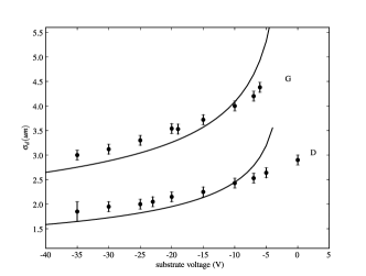
Hopkinson (1987) provides a theoretical model for the size of a charge diffusion cloud, , as a function of the operating voltage, V. This model starts from the assumption that the electron drift velocity is linearly proportional to the electric field strength at any height in the silicon an assumption we also adopt in Equation 2. Hopkinson (1987) predicts the final 1 radius of a charge cloud that begins at the surface of a CCD as:
| (6) |
where k is Boltzmann’s constant, T is the temperature of the CCD, is the electric permittivity of silicon ( F cm-1), e is the electron charge, and d is the thickness of silicon. is the concentration of acceptor atoms, which we determine from the resistivity values quoted in Table 1 using equation 1.24 from Janesick (2001, p.75). is the depletion depth, given by:
| (7) |
where V is the operating voltage of the device (approximately the gate voltage minus the substrate voltage). Figure 7 shows the data for CCD-D and CCD-G with the above model overplotted as solid lines. This figure demonstrates that the observed variation with and d is reasonably well matched by the Hopkinson model for large values of the substrate voltage. When is small, the devices approach underdepletion, so that the depletion depth, , is very close to the device thickness, d. Hopkinson’s model does not apply in this regime, which is why the data begin to deviate from the theory.
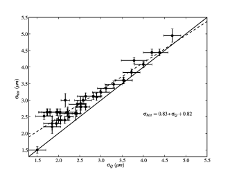
When comparing the two methods against each other, we find that they produce consistent, if not identical results. Figure 8 plots the measured value of against for all seven devices. If the two methods measured precisely the same value for the physical diffusion length, the points would fall along the solid line in this figure with a slope of one. A least squares fit to the points reveals a linear relation of the form , shown as the dashed line. As noted above, we have good reason to be suspicious of the accuracy of the histogram fitting model at very low values of . When is less than about 0.25, the prominent histogram features become crowded, leading to an inaccurate estimate of the diffusion length. This deficiency could be corrected by employing substantially more x-rays in the histogram to improve energy resolution and signal to noise.
6 Conclusions
Using a set of four devices with a range of thicknesses and charge collection characteristics, we have evaluated two methods for using x-rays to measure the amount of charge diffusion in CCDs. With a relatively simple model for the charge diffusion effect built off of the assumption of a Gaussian diffusion cloud, we are able to produce model histograms that match the observed pixel energy distributions very accurately. By varying the input parameters of the model to fit the observed data we can put precise constraints on both the amount of charge diffusion and the height of the barrier fields around each pixel. We introduce the Q ratio to measure the amount of diffusion based on a simple quotient of the outer eight pixels to the central pixel in the summed x-ray PSF. This method provides an even more direct means of assessing the diffusion properties of each device, as it requires no fitting procedure and is independent of model assumptions for relative diffusion measurements. Using the same model as for the histogram fitting method, we are able to turn this simple Q ratio into an absolute measurement of the size of the diffusion cloud. Comparing the fundamental diffusion parameters from each method, and , shows that the two methods produce results that are in good agreement. Due to the confusion of histogram features in low diffusion devices, is best for measuring relatively large values of and is more appropriate for the smaller values. X-ray images are easy to collect in the lab, requiring very little specialized equipment, and only minimal image processing is necessary to get the data needed for these techniques. All of these advantages make the x-ray histogram and PSF ratio methods very useful ”quick-look” additions to the CCD evaluation toolkit.
References
- Hopkinson (1987) Hopkinson G.R., Aug. 1987, Optical Engineering, 26, 766
- Janesick (2001) Janesick J.R., 2001, Scientific charge-coupled devices, Scientific charge-coupled devices, Bellingham, WA: SPIE Optical Engineering Press, 2001, xvi, 906 p. SPIE Press monograph, PM 83. ISBN 0819436984
- Kraft et al. (1995) Kraft R.P., Nousek J.A., Lumb D.H., et al., Feb. 1995, Nuclear Instruments and Methods in Physics Research A, 366, 192
- McCarthy et al. (1995) McCarthy K.J., Owens A., Holland A.D., Wells A.A., Feb. 1995, Nuclear Instruments and Methods in Physics Research A, 362, 538
- Pavlov & Nousek (1999) Pavlov G.G., Nousek J.A., Jun. 1999, Nuclear Instruments and Methods in Physics Research A, 428, 348
- Tonry et al. (1997) Tonry J., Burke B.E., Schechter P.L., Oct. 1997, PASP, 109, 1154
- Tsunemi et al. (1999) Tsunemi H., Hiraga J., Mori K., Yoshita K., Miyata E., Oct. 1999, Nuclear Instruments and Methods in Physics Research A, 436, 32