Electric Field Driven Domain Wall Dynamics in BaTiO3 Nanoparticles
Abstract
We report a detailed investigation into the response of single BaTiO3 (BTO) nanocrystals under applied electric fields (E-field) using Bragg Coherent Diffraction Imaging (BCDI). Our study reveals pronounced domain wall migration and expansion of a sample measure in situ under applied electric field. The changes are most prominent at the surface of the nanocrystal, where the lack of external strain allows greater domain wall mobility. The observed domain shifts are correlated to the strength and orientation of the applied E-field, following a side-by-side domain model from Suzana et al. Notably, we identified a critical voltage threshold at +10 V, which leads to irreversible structural changes, suggesting plastic deformation. The findings highlight how surface effects and intrinsic defects contribute to the enhanced dielectric properties of BTO at the nanoscale, in contrast to bulk materials, where strain limits domain mobility. These findings deepen our understanding of nanoscale dielectric behaviour and inform the design of advanced nanoelectronic devices.
I Introduction
In ferroelectric materials like BTO, the electric polarisation is inherently linked to the crystal structure where the titanium (Ti4+) ion is displaced from the unit cell centre, creating a dipole along the c-axis in the room-temperature tetragonal phase. For example, nanosized BTO particles show a significant enhancement of their dielectric constant, sufficient for widespread commercial applications in multilayer ceramic capacitors (MLCC) Curecheriu2010 . Wada et al. Wada2003 performed powder dielectric measurements on various BTO particles ranging from 17 to 100 nm. Their study showed the BTO particle with a size of 70 nm has the best dielectric constant, around 15000, meaning it is ideal for storing electric energy. Our study examine the dielectric response of hydrothermally synthesised BaTiO3 nanoparticles, particularly focusing on their behaviour under varying electric fields and domain configurations.
The fundamental nature of the dielectric response in materials involves the displacement of charges proportional to an applied electric field. In ferroelectrics, this response is further complicated by the permanent polarisation that is not only dependent on the applied field but also intimately tied to the structural phase of the material. BTO, for instance, typically exists in a high symmetric (non-ferroelectric) cubic phase at high temperatures but transforms into a low symmetric tetragonal phase when the temperature drops below the Curie temperature around 398 Comes1970 ; Zhong1994 .
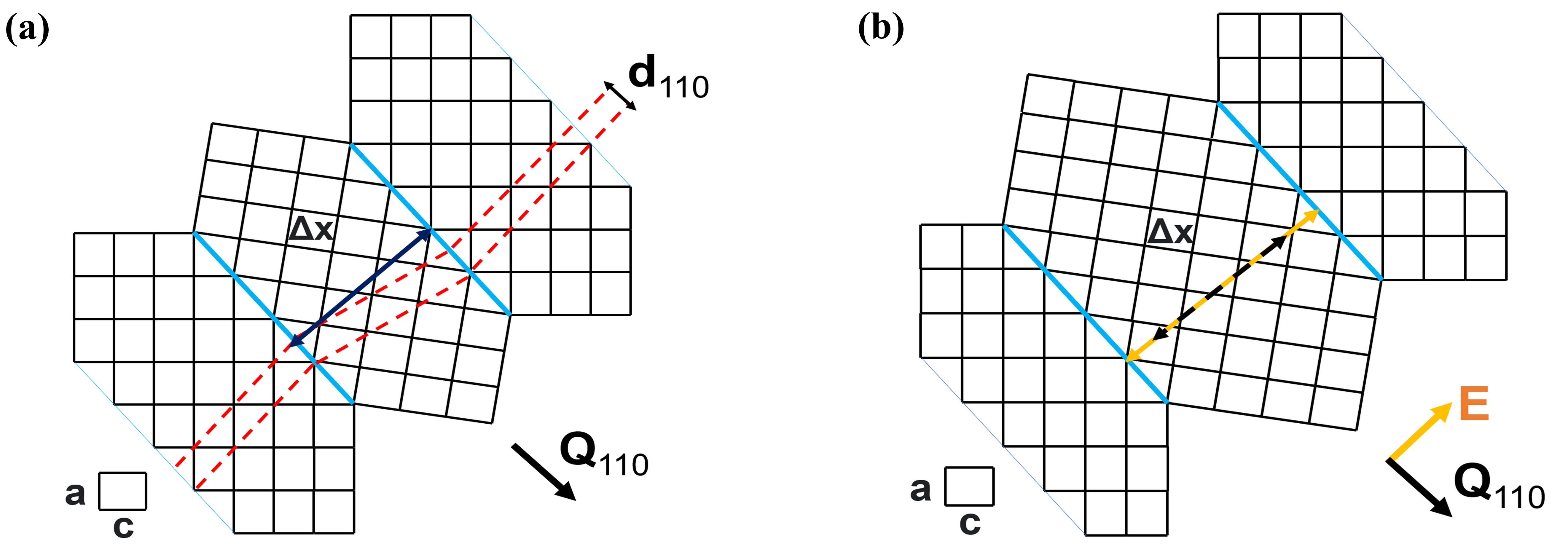
Models have been proposed to elucidate the enhanced dielectric behaviour observed in nano-scale BTO. These models include, (1) A sudden switch of polarisation within domains, such as a 90-degree rotation, which reflects a dramatic reorientation of the polarisation direction Mimura2016 . (2) Modulation of the polarisation direction by altering the displacement of the Ti4+ ion within the crystal lattice, potentially enhancing or suppressing the overall polarisation Rudel2020 . (3) The migration of domain walls, which could be influenced by external factors such as the application of an electric field or mechanical stress, leading to configurations like side-by-side domain arrangements as proposed by Suzana et al. Suzana2023 ; Diao2020 or in core-shell configurations Hoshina2008 ; Hoshina2013 .
Suzana et al. Suzana2023 introduced a side-by-side model as illustrated in Figure 1 (a), detailing the structural characteristics of hydrothermally-synthesised BTO nanoparticles. Comprehensive X-ray diffraction (XRD) analyses found that specific batches of BaTiO3 samples displayed a mixture of both tetragonal and cubic phases Suzana2023 . Interestingly, it emerged that the cubic phase was the one that demonstrates a higher dielectric constant in these samples. A comparative analysis between cubic and tetragonal preparations of similar particle size revealed a notable discrepancy: cubic particles exhibited a considerably higher degree of “microstrain” in the Williamson-Hall analysis Williamson1953 of their powder diffraction patterns. Moreover, the examination of local structure using X-ray pair distribution function (PDF) analysis Kwei1995 ; Senn2016 revealed a lower symmetry consistent with tetragonal arrangements Suzana2023 . Cubic BTO should not be stable at room temperature, but appears to be stabilised in the granular material by mutual strain between nano-domains with tetragonal structure.
Bragg coherent diffraction imaging (BCDI) Robinson2001 ; Robinson2006 is a powerful technique for probing strain within single nanocrystals. When a crystal is sufficiently smaller than the coherent beam Clark2012 , typically less than , BCDI can generate high-resolution 3D maps of complex electron density. The amplitude of numbers reflects the “Bragg density”, indicating the strength of diffraction for a specific Bragg peak, while the phase represents the projection of local lattice displacement along the Bragg peak direction Diao2017 . The phase , associated with the crystal displacement vector , is given by the relation Robinson2009 :
| (1) |
where is the momentum transfer vector of the Bragg peak. The BCDI image and the diffraction pattern are related by a 3D Fourier transform. The diffraction pattern is an array of complex numbers, of which the phase information cannot be directly measured because pixelated detectors only record the magnitude of the diffraction pattern, giving rise to the famous “phase problem” Robinson2006 ; Williams2003 .
Despite this challenge, the phase of the diffraction pattern is encoded within the diffraction fringes, and iterative phase retrieval algorithms have been developed to recover it Gerchberg1972 ; Fienup1982 . These algorithms apply constraints in both real and reciprocal space to refine the phase information Fienup1978 ; Fienup1986 ; Yang2022 . A prerequisite for successful phase retrieval is oversampling. According to Bates (1982) Bates1982 , the fringe spacing of the diffraction pattern must exceed twice the Nyquist frequency, in line with Sayre’s interpretation Sayre1952 of Shannon’s information theorem Shannon1948 .
Remarkably, when imaged using BCDI, it was evident that individual BTO nanoparticles invariably contained multiple domains, each displaying spatially varying strain Suzana2023 . This led to the model-based prediction as shown in Figure 1 (b), linking the domain structure within BTO nanoparticles to the dielectric enhancement of BTO nanocrystals. When exposed to an electric field, these domains would undergo a growth and shrinkage response, rather than reorientation of the domain c-axes. This energy-efficient response requires no ionic diffusion, so the behaviour might contribute to the extended service lifetimes and superior high-frequency performance observed in commercial nano-BTO MLCCs. Our investigation here employs operando electric field BCDI measurements which confirm this model.
II EXPERIMENTAL METHODS
II.1 Hydrothermal Synthesis
We synthesised high-quality nanocrystals, approximately 200 nm in size, using hydrothermal methods Suzana2023 .These samples were prepared in an autoclave at 240 °C nominal temperature from starting solutions of TiCl4 and BaCl2. They were stirred and mixed in a 50 mL 2 neck round bottom flask. NaOH in 10 mL of deionised water was then added to the system. The whole growth process took place in an autoclave for 48h. The detailed procedure was described by Suzana et al Suzana2023 .
Predominantly, these BTO 240 °C crystals were found to be in the cubic phase, understood to be a strained composite of tetragonal domains Suzana2023 . We then deposited these nanocrystals onto gold interdigital electrode arrays with 3-micrometer spacing, following the methodology of Kim et al. Kim2004 . Particles were drop-cast and seamlessly bonded into a continuous film using Tetraethyl orthosilicate (TEOS), followed by a process of annealing Monteforte2016 . This method was developed to stabilise the particles for BCDI experiments, while preventing dielectric leakage and ensured a uniform electric field throughout the dielectric particles. Examples of the samples used are shown in Fig 2 (a).

II.2 Scanning X-ray Diffraction Microscopy (SXDM)
In Figure 2 (a), these electrodes, arranged vertically and perpendicular to the x-ray beam that came from 001 direction, and generated electric field in the z direction. The alignment microscopes at ID-01 enabled the selection of “crowded” regions of particles which bridge the electrodes without gaps, so the full field was seen by the target crystal. By selecting densely clustered BTO particles for the measurement, we minimised capacitance loss due to air exposure and enhanced the electric field response between domain walls. SXDM was then employed to scan locally for crystals that responded to changes in the applied electric field. As shown in Figure 2 (a), this method divided the confocal microscope field of view into an 80 m by 80 m region (red box). A raster scan was performed from the top left to the bottom right of the box. The detector was placed according to the calculated [110] 2 position, and picked up intensity once a crystal was illuminated during the raster. SXDM was then repeated with an applied electric field. Crystals that responded to the electric field exhibited intensity changes, while those that did not remained neutral. Figure 2 (b) displays the net intensity differences before and after applying the electric field, with variations between 10V direct current (DC) indicated by positive and negative colours.
II.3 BCDI Experiment
By applying safe voltages up to 10V DC, we could achieve fields up to 3MV/m. This allowed us to investigate the rearrangements of internal domain wall structures using BCDI at beamline ID-01 of the European Synchrotron Radiation Facility (ESRF), utilising x-rays with an energy of 10.5 keV ( 0.118 nm). The sample was mounted on a 3-axis goniometer with the Maxipix detector (55 55 pixels) placed 0.586 m away. 3D BCDI data were collected as rocking curves of detector frames with a step size of with a 1 s exposure time. The voltage scans are measured in (0 V, 10 V, -5 V, 5 V, -10 V, 0 V) sequence to eliminate any systematic uncertainties. We ensured reproducibility by measuring each crystal twice before changing voltage levels. To account for potential crystal motion during measurements, we employed sub-pixel cross correlation Guizar2008 processes for pattern alignment. This method provided a more accurate interpretation of crystal behaviours under variable electric fields.
III Computational models
III.1 Guided Algorithm (GA)
We used a guided error reduction (ER) and relaxed averaged alternating reflections (RAAR) algorithm Luke2005 , in conjunction with the shrinkwrap (SW) approach Marchesini2003 , to reconstruct BTO nanoparticles. The SW algorithm utilised a Gaussian fill function. To ensure uniqueness and reliability of the reconstruction, we incorporated multiple random starts in a guided algorithm (GA) framework that leveraged genetic breeding techniques Chen2007 . For the GA, we utilised a population of 100 with 5 generations of breeding. In each generation, the “avg-half” method was used, which computes the average across the better half of the population Ulvestad2017 . The breeding mode “avg_ab” combines the best population iterate (“a”), determined by GA metrics, with the current population iterate (“b”), using a geometric mean Clark2015 .
To reduce noise, the diffraction pattern data were binned by a factor of two along each axis of the detector plane. The SW threshold was varied between 12% and 15%, consistently yielding reconstructions with Chi square () values (Eq. 2) between 1.6% and 1.8%. The final model was reconstructed using a 12% SW threshold, achieving a of 1.62%.
III.2 Phase Transfer Algorithm (PTA)
To visualise the structural changes in real space, we need to invert the diffraction patterns to images. Previously it has been effective to use a Difference Fourier Algorithm (DFA) Henderson1971 ; Watari2011 . The DFA is based on the idea that each missing phase of the diffraction pattern has contributions from every point in the real space object; hence if there is a small local change of structure, the diffraction phase is almost unchanged and can be transferred to the measured diffraction amplitude. When we calculated real-space images by DFA, we found there were no localised features in the images, so concluded it was insensitive to the kind of domain-wall motions expected.
We then employed a Phase Transfer Algorithm (PTA) instead: a single reconstruction was carried out and the diffraction phases were transferred to the data measured at the other voltages. Like for the DFA, this served to reduce inconsistencies which might have arisen from noise propagation effects resulting in spurious differences between separate reconstructions. We note that these are phase domain structures, strong real-space phase objects, which are hard to reconstruct reliably. The PTA avoids the small variations between the different reconstructions (from random starts) by using just one solution to phase the structural differences.
The comparison of diffraction patterns, both between measurements and with reconstructed models employs metrics such as the Chi square and Pearson correlation coefficient (PCC) as defined below:
| (2) |
| (3) |
where A and B are data arrays of model diffraction pattern and experimental data.
The PTA approach we used involves employing a Genetic Algorithm (GA) in MATLAB to reconstruct the merged diffraction patterns of the crystal at different applied electric fields. Instead of starting from a random phase, we used the single merged 0V reconstruction, described above, as the initial guess for subsequent voltage scans. This ensured consistent results and avoided reproducibility issues. For each voltage scan, guided ER and RAAR algorithms introduced in Section III.1 were performed until the algorithm converged, accurately capturing the structural evolution of the BTO sample under different voltage levels. The resulting reconstructions yielded values of 7.54% (10V), 4.65% (5V), 1.42% (0V), 3.16% (-5V), and 3.66% (-10V).
III.3 c/a ratio from domain phases
Our side-by-side model from Figure 1 (a) and (b) predicts a shift of domain walls under applied electric fields to enlarge the domains polarised parallel to the field. This process should not change the unit cell structure, meaning a constant ratio between the lattice parameter. The ratio of the lattice parameter follows the equation below Suzana2023 :
| (4) |
where and are the positive and negative slope of the phase; and are the thickness of the domain corresponding to the phase changes. The derivation of Eq. 4 is provided in the Appendix A. The lattice parameter of BTO 240 °C at room temperature are: a = 3.9942 Å, c = 4.0305 ÅSuzana2023 ; Billinge2007 . The c/a ratio is therefore 1.0091.
IV Results
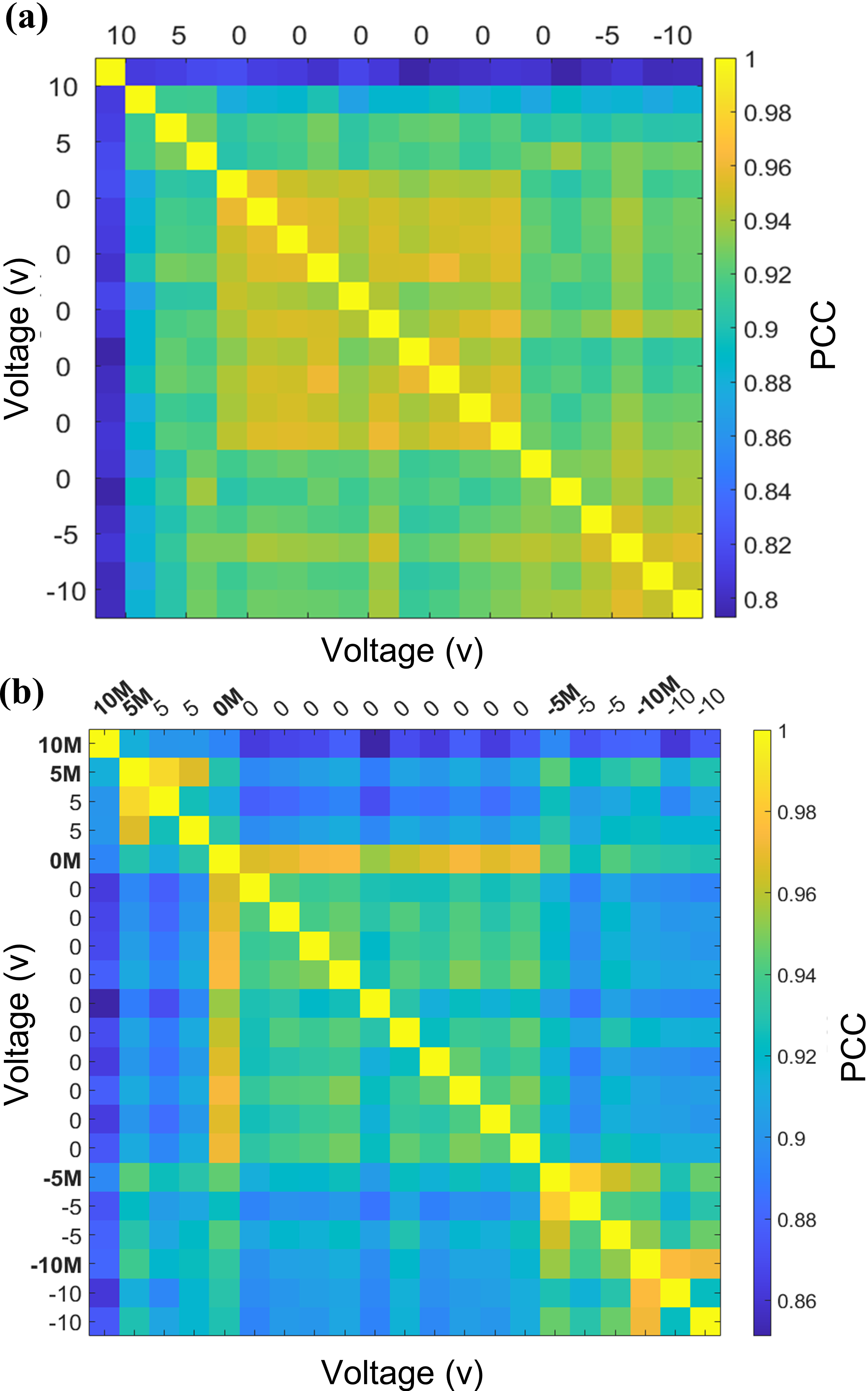
The result is shown in Figure 3 (a) which compares all the measured diffraction patterns under varying electric field strengths using PCC (Eq. 3) method. Each scan is compared with the rest of the voltage scans, presented as a 20 by 20 heat colour map. Results are set in an ordered sequence from 10 V to -10 V.
At 0 volts, PCC values were high (above 0.94), indicating a good consistency of the measurement. These minor differences observed can be attributed to systematic errors inherent in BCDI measurements, such as beam stability or sample positioning variations. However, at and volts, there was a notable shift: PCC values decreased to as low as 0.79. This significant change in diffraction patterns suggests a voltage-induced alteration in the BTO crystal domain structure. Additionally, we removed three outliers, one in the initial 10 V scan and discrepancies in the last two 0 volt scans. These might arise due to sample damage or dielectric breakdown from the high voltages.
After the outliers were excluded to ensure consistency, the scans with identical voltage levels were merged together by cross correlation using sub-pixel shifts, enhanced the signal-to-noise ratio of the data. The PCC heat map in Figure 3 (b) presents the merged scan data, showing clearer differentiation between voltage regions. This improved our ability to observe the subtle structural changes within the BTO nano-crystal under varied electric fields.
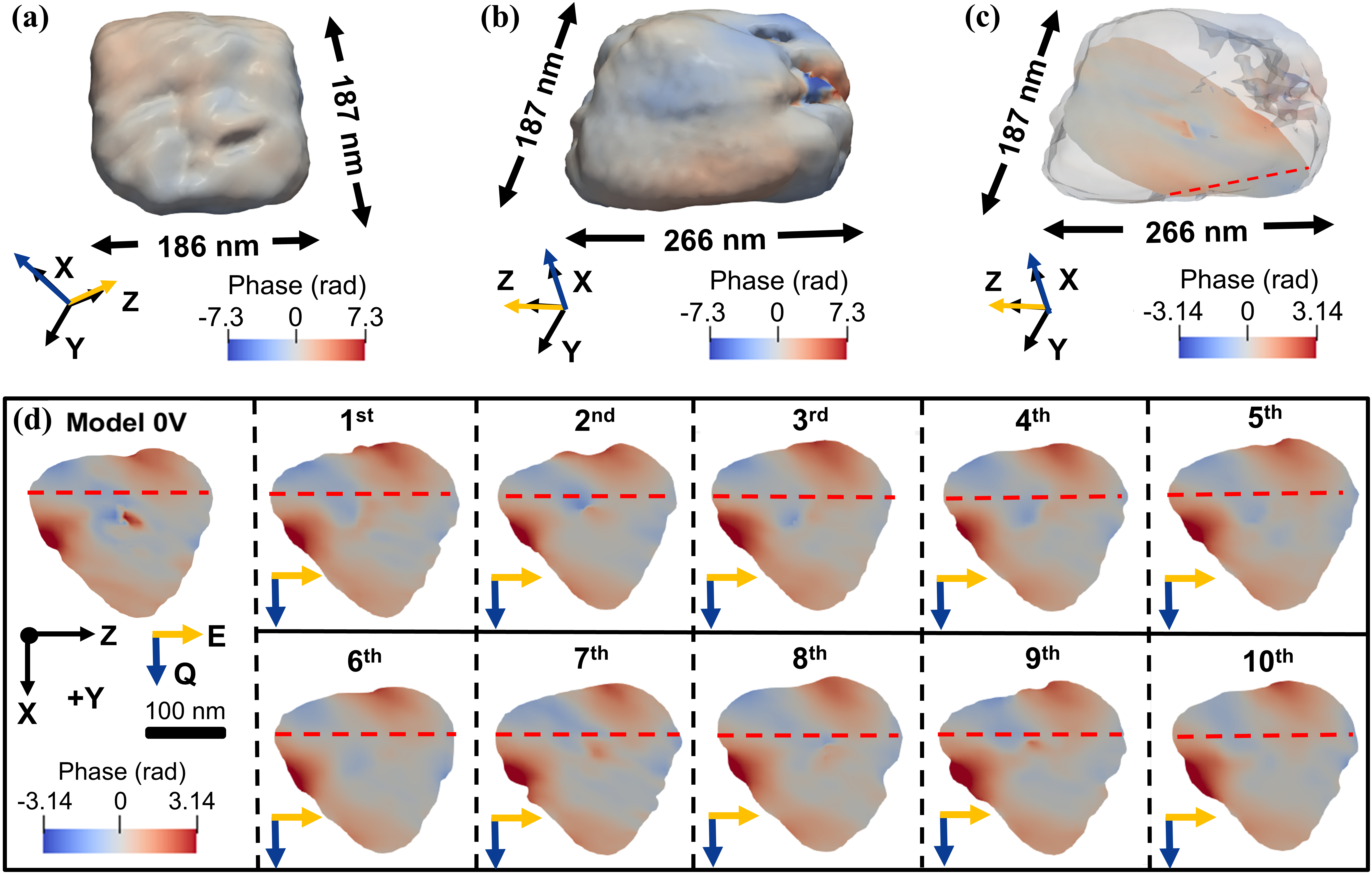
The merged scan labelled ‘0M’ is the sum of the ten 0 V diffraction pattern with consistent PCC values from 0.94 to 0.98. This merged scan was subjected to phase reconstruction as discussed in section III A. Its solution becomes the reference structure input for the PTA. Figure 4 (a) and (b) show the 3D reconstruction of the diffraction pattern of the merged 0 V scan. The sample has a rectangular shape with dimensions of in length and width, and in height. The nanocrystal size varies depending on the SW threshold, ranging from 12% to 15%. A cross-section in the XZ plane is shown in panel (c), where the positive red phase indicates regions of the crystal displaced in the direction of the vector, while the negative blue represents displacement in the opposite direction. The same slice in panel (d), labelled “Model 0V”, further highlights strain patterns at the central region, suggesting the presence of a dislocation loop. This dislocation serves as a fiducial marker when comparing reconstruction slices of the same crystal under different voltages. This slice was selected because it aligns with the applied voltage along the z-axis, where domain wall motion is expected. This allows evaluation of PTA consistency, as the phase along the red dashed line should remain uniform at 0V.
To assess the consistency of our PTA, we analysed the phase reconstruction patterns of 10 separate zero voltage scans. Figure 4 (d) displays the zero voltage phase maps obtained sequentially from the experiment, demonstrating similar patterns. Phase values extracted along a line from these maps, chosen to cross several domains, were used to evaluate domain size consistency across reconstructions.
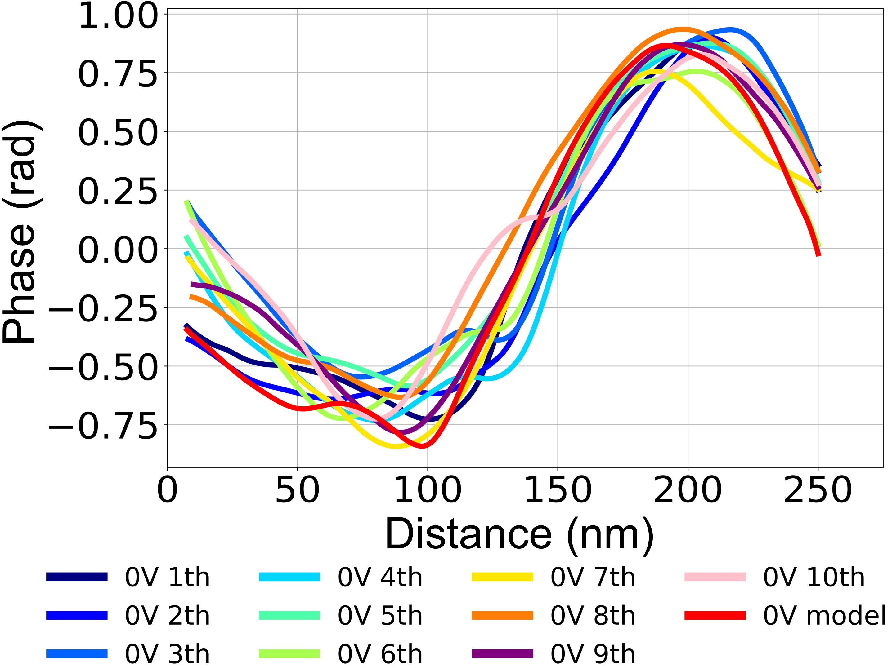
Figure 5 shows a close similarity with the triangular phase profiles seen by Suzana et al. Suzana2023 . Minor variations in slope are observed between 0 and 100 nm, likely due to noise. These deviations are more pronounced at the edges of the nanocrystal. The phase profile in Figure 5, corresponding to the red dashed line in the schematic (Figure 1 (a)), shows maxima and minima that indicate domain boundaries, aligning with the blue lines in Figure 1 (a). The distance between these extrema represents domain thickness, measured at approximately 100 nm. The ratio, derived from phase changes over these domain distances, yields a mean of 1.00052 with a standard deviation of 5.9 × 10⁻⁵, closely matching the reference ‘Model 0V’ value of 1.00056. This strong agreement validates the reliability of our comparison algorithm for zero voltage conditions. When a voltage is applied, domain wall motion is expected to shift these extrema horizontally, while maintaining a consistent linear slope, as will be discussed in the following section.
V Phase Profile
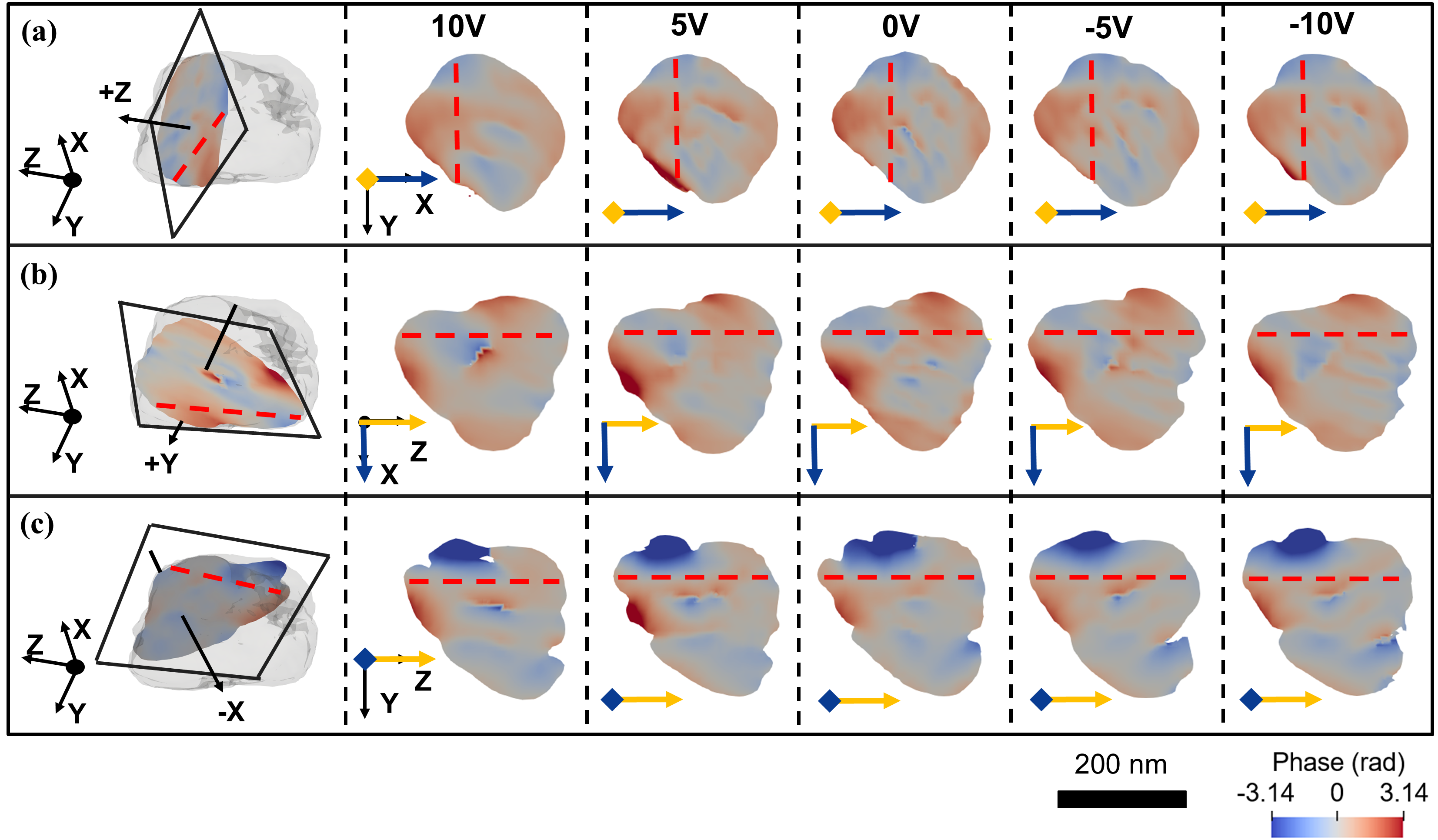
Figure 6 (a-c) displays domain structures within the same BTO nanoparticle under different voltages. The vector points along the [110] direction. The dashed red lines indicate the locations of the extracted phase plots, perpendicular to the vector. These choices are aimed at determining whether the domain expansion is driven by the applied electric field. The reconstructed nanocrystals at each voltage are aligned using the center of mass (COM) method to ensure consistent comparisons across voltages. As mentioned previously, slices were aligned on a common central dislocation loop used as a fiducial marker.
In the X view of the YZ plane, a triangle-shaped wave of in-plane shifts is seen to respond to the E-field. Similarly, the Y view of the XZ plane shows migrated domain stripes due to out-of-plane shifts with increasing E-field. However, the Z view of the XY plane shows no significant response. This suggestion of orientation-dependent domain behaviour is discussed below. The domain migration occurs predominantly along the Z-axis, which is further analysed in the phase plots below.
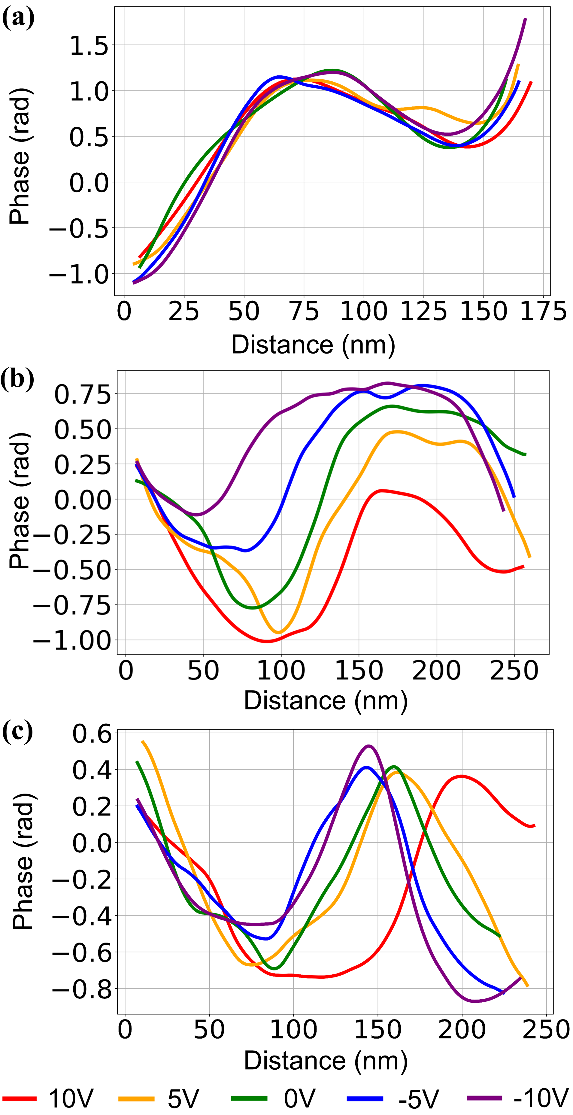
Figure 7 (a) illustrates the phase plot in the plane, where the domains remain stable, with a mean c/a ratio of 1.00081 (from slope, see Appendix A) and a standard deviation of 4.2 × 10⁻⁵.
In contrast, Figure 7 (b) highlights the most pronounced domain size changes and migration in a slice of the XZ plane. Under applied voltages, the domains extend up to 135 nm deep from the particle surface along the z-axis. At 5 V and 10 V, the phase-positive domain contracts by 25 nm and 35 nm, respectively, whereas it expands by 20 nm and 100 nm under 5 V and 10 V. The mean c/a ratio is calculated as 1.00078 with a standard deviation of 6.3 × 10⁻⁵.
Figure 7 (c) also illustrates significant motions of domain walls in a YZ plane slice. At 10 V, the phase-positive domain migrates from 160 nm to 200 nm along the z-direction of the slice, while it shifts back to 145 nm at 5 V and 10 V. Likewise, the phase-negative domain migrates from 85 nm to 145 nm at 10 V and reverses by 10 nm at 5 V and 10 V. Migration effects are less pronounced at 5 V. The mean c/a ratio in this plane is 1.00066, with a standard deviation of 8.3 × 10⁻⁵.
VI Discussion
Our study offers new insights into the response of BTO nanocrystals under applied electric fields, employing BCDI to capture real-time domain behaviour at the nanoscale. With the electric field oriented approximately along the z-axis and the vector positioned around 12 degrees off the x-axis, our results show a direct correlation between electric field strength and domain wall migration. The diffraction patterns in Figure 3 (a) demonstrate a clear dielectric response to the external field, while the phase profiles in Figure 7 reveal substantial domain wall shifts and expansions. Notably, the consistent c/a ratios (ranging from 1.00066 to 1.00081) across all planes confirm the structural stability of the material, even under dynamic conditions.
BCDI real-space reconstructions in Figure 7 (b-c) clearly illustrate pronounced domain expansions and shifts along the z-axis, particularly in the XZ (+Y) and YZ (-X) plane slices. This behaviour can be attributed to the alignment of the vector perpendicular to these planes, and phase lines parallel to the E-field, which maximises the observed effects. Conversely, no significant domain wall motion was detected when phase lines were perpendicular to the E-field, indicating an orientation-dependent response. The most significant domain wall motion occurred perpendicular to the vector, driven by the E-field along the z-axis.
We selected the red dashed lines in the phase plots (Figure 6 b,c and Figure 7 b,c) to capture the regions of most significant phase shifts, which occurred predominantly at the surface of the BTO nanocrystals. This can be attributed to the nearly strain-free nature of the open surfaces, allowing domain walls to move more freely compared with those in the interior, where domains are constrained by strain and more tightly locked. This higher degree of freedom for domain motion at the surface may explain why nano-sized BTO exhibits a higher dielectric constant than bulk materials, a phenomenon first discovered by Wada et al. Wada2003 . In contrast, the strain in bulk materials restricts the motion of domain walls, limiting this mechanism of dielectric response.
While the domain shifts remained largely reversible across various electric field strengths, a notable loss of reversibility was observed at the highest voltage (10 V). As depicted in Figure 3 (a), the diffraction patterns at 0V exhibited permanent changes after applying 10 V. This suggests that 10 V represents a critical threshold, beyond which the influence of the electric field on the crystal structure becomes pronounced, showing plastic deformation. At such extreme voltages, the mechanisms driving domain migration may shift from purely reversible electric field effects to irreversible and might be a structural explanation of dielectric break down. Some other regions with steep slopes (high c/a ratio) in the phase plots further indicate that additional factors, such as intrinsic defects, may contribute to the limited reversibility of domain behaviour.
Our study confirms the side-by-side model of domain wall migration under external E-field and highlights critical thresholds for significant structural changes in BTO nanocrystals. Furthermore, this work provide insight into explain the enhanced dielectric response of nano-sized materials. These findings hold significant implications for future applications in nanoelectronic devices and materials engineering, where controlling domain behaviour and dielectric properties at the nanoscale is crucial.
Acknowledgements
We acknowledge the ESRF for the provision of synchrotron radiation facilities under proposal number HC-5370 utilising beamline ID01. The DOI for the data measured at ESRF is 10.15151/ESRF-ES-1199261421. Work at Brookhaven National Laboratory was supported by the U.S. Department of Energy, Office of Science, Office of Basic Energy Sciences, under Contract No. DESC0012704.
Appendix A
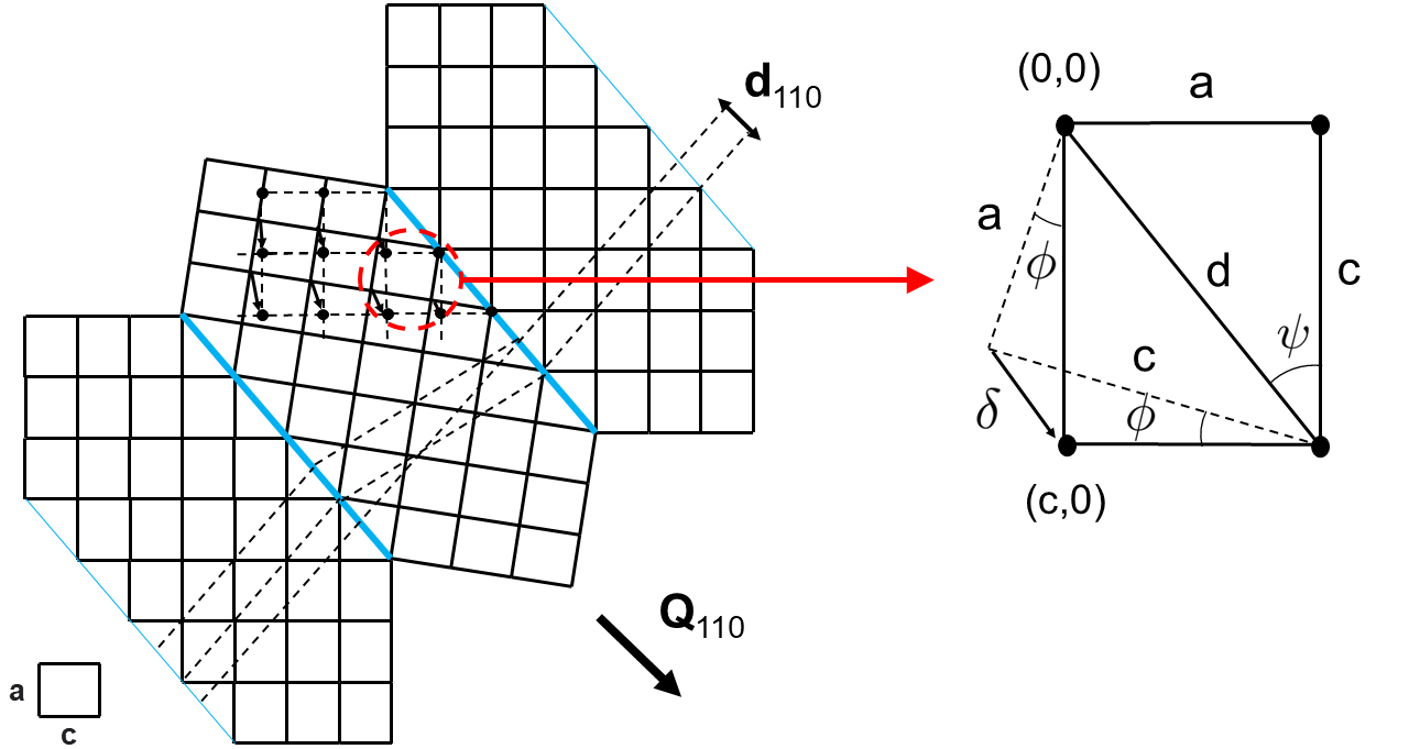
The trigonometric relations can be written as:
| (5) |
The shift is therefore given by:
| (6) |
Starting with the definition of and proceeding with the simplifications using Eq. 7:
| (7) |
| (8) |
Taking the positive root,
| (9) |
The resulting can be used to calculate the displacement over a lateral distance :
| (10) |
The phase introduced by the displacement is:
| (11) |
Rearrange to get c/a ratio:
| (12) |
Where and are the positive and negative slope of the phase; and are the thickness of the domain corresponding to the phase changes.
References
- (1) A. F. Suzana, S. Liu, J. Diao, L. Wu, T. A. Assefa, M. Abeykoon, R. Harder, W. Cha, E. S. Bozin, and I. K. Robinson, Structural Explanation of the Dielectric Enhancement of Barium Titanate Nanoparticles Grown under Hydrothermal Conditions, Advanced Functional Materials 33, 2208012 (2023).
- (2) L. Curecheriu, M. T. Buscaglia, V. Buscaglia, Z. Zhao, L. Mitoseriu, Appl. Phys. Lett. 97, 242909 (2010).
- (3) S. Wada, H. Yasuno, T. Hoshina, S. Nam, H. Kakemoto, T. Tsurumi, Preparation of nm-Sized Barium Titanate Fine Particles and Their Powder Dielectric Properties, Japanese Journal of Applied Physics 42, 6188 (2003).
- (4) W. Zhong, D. Vanderbilt, and K. M. Rabe, Phase Transitions in BaTi from First Principles, Phys. Rev. Lett. 73, 1861–1864 (1994).
- (5) R. Comès, M. Lambert, and A. Guinier, Linear disorder in crystals (case of silicon, quartz, and ferroelectric perovskites), Acta Crystallographica Section A 26, 244–254 (1970).
- (6) K. Mimura, Processing of dielectric nanocube 3D-assemblies and their high electrical properties for next-generation devices, Journal of the Ceramic Society of Japan 124, 848-854 (2016).
- (7) H. Rudel, M. Lane, C. Muhich, and J. Zimmerman, Toward Informed Design of Nanomaterials: A Mechanistic Analysis of Structure-Property-Function Relationships for Faceted Nanoscale Metal Oxides, ACS Nano, (2020).
- (8) J. Diao, X. Shi, T. A. Assefa, L. Wu, A. F. Suzana, D. S. Nunes, D. Batey, S. Cipiccia, C. Rau, R. J. Harder, W. Cha, and I. K. Robinson, Evolution of ferroelastic domain walls during phase transitions in barium titanate nanoparticles, Phys. Rev. Mater. 4, 106001 (2020).
- (9) T. Hoshina, S. Wada, Y. Kuroiwa, and T. Tsurumi, Composite structure and size effect of barium titanate nanoparticles, Applied Physics Letters 93, 192914 (2008).
- (10) T. Hoshina, Size effect of barium titanate: Fine particles and ceramics, J. Ceram. Soc. Jpn. 121, 156 (2013).
- (11) G.K Williamson and W.H Hall, X-ray line broadening from filed aluminium and wolfram, Acta Metallurgica 1, 22-31 (1953).
- (12) G. H. Kwei, S. J. L. Billinge, S. -W. Cheong, and J. G. Saxton, Pair-distribution functions of ferroelectric perovskites: Direct observation of structural ground states, Ferroelectrics 164, 57 (1995).
- (13) M. S. Senn, D. A. Keen, T. C. A. Lucas, J. A. Hriljac, and A. L. Goodwin, Emergence of long-range order in BaTiO3 from local symmetry-breaking distortions, Phys. Rev. Lett. 116, 207602 (2016).
- (14) I. K. Robinson, I. A. Vartanyants, G. J. Williams, M. A. Pfeifer, and J. A. Pitney, Reconstruction of the Shapes of Gold Nanocrystals Using Coherent X-Ray Diffraction, Phys. Rev. Lett. 87, 195505 (2001).
- (15) M. A. Pfeifer, G. J. Williams, I. A. Vartanyants, R. Harder, and I. K. Robinson, Three-dimensional mapping of a deformation field inside a nanocrystal, Nature 442, 63–66 (2006).
- (16) J. Clark, X. Huang, R. Harder, and I. Robinson, High-resolution three-dimensional partially coherent diffraction imaging, Nat. Commun., 3, 993 (2012).
- (17) J. Diao, B. Chen, Q. Luo, W. Lin, X. Liu, J. Shen, and I. Robinson, Nucleation of fractal nanocrystallites upon annealing of Fe-based metallic glass, Journal of Materials Research, 32, 1–8 (Mar. 2017).
- (18) I. Robinson and R. Harder, Coherent Diffraction Imaging of Strains on the Nanoscale, Nature Matls, 8, 291–298 (2009).
- (19) G. J. Williams, M. A. Pfeifer, I. A. Vartanyants, and I. K. Robinson, Three-dimensional imaging of microstructure in Au nanocrystals, Phys. Rev. Lett., 90, 17 (May 2003).
- (20) R. W. Gerchberg, A practical algorithm for the determination of phase from image and diffraction plane pictures, Optik, 35, 237–246 (1972).
- (21) J. R. Fienup, Phase retrieval algorithms: a comparison, Applied Optics 21, 2758-2769 (1982).
- (22) J. R. Fienup, Reconstruction of an object from the modulus of its Fourier transform, Opt. Lett., 3, 27–29 (July 1978).
- (23) J. R. Fienup and C. Wackerman, Phase-retrieval stagnation problems and solutions, Journal of the Optical Society of America A 3, 1897-1907 (1986).
- (24) D. Yang, N. W. Phillips, K. Song, C. Barker, R. J. Harder, W. Cha, W. Liu, and F. Hofmann, In situ Bragg coherent X-ray diffraction imaging of corrosion in a Co-Fe alloy microcrystal, 2022.
- (25) R. Bates, Fourier phase problems are uniquely solvable in more than one dimension. I: underlying theory, Optik (Stuttgart), 61, 247–262 (1982), p. 5.
- (26) D. Sayre, Some implications of a theorem due to Shannon, Acta Crystallographica, 5, 843–843 (1952).
- (27) C. E. Shannon, A mathematical theory of communication, The Bell System Technical Journal, 27, 379–423 (1948).
- (28) Y Kim, and J. K. Jung, and K. S. Ryu, Structural study of nano BaTiO3 powder by Rietveld refinement, Materials Research Bulletin 39, 1045-1053 (2004).
- (29) M. Monteforte, A. K. Estandarte, B. Chen, R. Harder, M. H. Huang, and I. K. Robinson, Novel silica stabilization method for the analysis of fine nanocrystals using coherent X-ray diffraction imaging, J Synchrotron Radiat 23(4), 953-958 (2016).
- (30) M. Guizar-Sicairos, S. T. Thurman, and J. R. Fienup, Efficient Subpixel Image Registration Algorithms, Opt. Lett. 33, 156-158 (2008).
- (31) D. R. Luke, Relaxed averaged alternating reflections for diffraction imaging, Inverse Problems 21, 37 (2005).
- (32) S. Marchesini, H. He, H. N. Chapman, S. P. Hau-Riege, A. Noy, M. R. Howells, U. Weierstall, and J. C. H. Spence, X-ray image reconstruction from a diffraction pattern alone, Physical Review B 68, 140101 (2003).
- (33) C. C. Chen, J. Miao, C. W. Wang, and T. K. Lee, Application of optimization technique to noncrystalline x-ray diffraction microscopy: Guided hybrid input-output method, Physical Review B 76, 064113 (2007).
- (34) A. Ulvestad, Y. Nashed, G. Beutier, et al., Identifying Defects with Guided Algorithms in Bragg Coherent Diffractive Imaging, Scientific Reports 7, 9920 (2017).
- (35) J. Clark, J. Ihli, A. Schenk, et al., Three-dimensional imaging of dislocation propagation during crystal growth and dissolution, Nature Materials 14, 780–784 (2015).
- (36) Richard Henderson and J. Moffat, The difference Fourier technique in protein crystallography: Errors and their treatment, Acta Crystallographica Section B Structural Crystallography and Crystal Chemistry 27, 1414-1420 (1971).
- (37) M. Watari, R. McKendry, M. Vögtli, G. Aeppli, Y. Soh, X. Shapiro-Shi, G. Xiong, X. Huang, R. Harder, and I. Robinson, Differential stress induced by thiol adsorption on facetted nanocrystals, Nature Materials 10, 862-6 (2011).
- (38) S. J. Billinge and I. Levin, The problem with determining atomic structure at the nanoscale, Science 316, 561-565 (2007).