Buried Dirac points in Quantum Spin Hall Insulators: Implications for edge transport and Majorana Kramer Pairs
For heterostructures formed by a quantum spin Hall insulator (QSHI) placed in proximity to a superconductor (SC), no external magnetic field is necessary to drive the system into a phase supporting topological superconductivity with Majorana zero energy states, making them
very attractive for the realization of non-Abelian states and fault-tolerant qubits.
Despite considerable work investigating QSHI edge states, there is still an open question about their resilience to large magnetic fields and the implication of such resilience for the formation of a quasi-1D topological superconducting state.
In this work, we investigate the transport properties of helical edge states in a
QSHI-SC junction formed by a
InAs/GaSb (15nm/5nm) double quantum well and a superconducting tantalum (Ta) constriction.
We observe a robust conductance plateau up to 2 T, signaling resilient edge state transport. Such resilience is consistent with the Dirac point for the edge states being buried in the bulk valence band.
Using a modified Landauer-Büttiker analysis, we find that the conductance is consistent with 98% Andreev reflection probability owing to the high transparency of the InAs/GaSb–Ta interface.
We further theoretically show that a buried Dirac point does not affect the robustness of
the quasi-1D topological superconducting phase,
and favors the hybridization of Majorana Kramer pairs and fermionic modes in the QSHI resulting in extended MKP states, highlighting the subtle role of buried Dirac points in probing MKPs.
Introduction
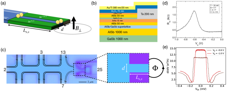
A quantum spin Hall insulator is a 2D topological insulator hosting a pair of time reversal symmetry-protected helical edge states 1, 2, 3, 4. The interplay of quantum Hall edge states and superconductivity has been extensively investigated with the prospect of realizing a topological superconductor 5, 6, 7, 8, 9, 10, 11, 12, 13, 14, 15 wherein exotic non-Abelian anyons called Majorana zero modes (MZM), which can be used to construct topological qubits for topological quantum computing 16, 17, 18, are predicted to exist. However, their unambiguous experimental demonstration remains elusive 19, 20, 21, 22, 23, 24, 25, 26, 27, 28, 29. Recently, it was suggested that Majorana Kramer pairs 30 (MKPs) can be used to create a “Majorana Kramer pairs qubit,” which may be a viable alternative to MZM-based qubits 31. To assess the potential of a qubit based on MKPs, theoretical analysis of realistic models and experimental investigation of prospective devices are needed. MKPs have been predicted in QSHI-SC hetrostructures with a quantum point contact (QPC) where helical edge states hybridize at a QPC, see Fig. 1 (a). When the SC constriction is phase-biased by a flux (where is the superconducting magnetic flux quantum), MKPs can form at the ends of the constriction 32, 33.
In this work, we theoretically and experimentally investigate MKPs in a QSHI with a flux-biased superconducting constriction. We measure a quantized three-terminal conductance of in an InAs/GaSb(15nm/5nm) double quantum well across a superconducting Ta constriction. We then apply an out-of-plane magnetic field and observe little variation in the sub-gap conductance up to T. Analyzing the conductance with a modified Landauer-Büttiker model accounting for Andreev reflection of helical edge states, we find the conductance measured is consistent with nearly perfect Andreev reflection (), owing to the high quality of the device and the helical edge state properties. Performing numerical simulations of edge state transport using the Bernevig-Hughes-Zhang (BHZ) model 4 within the Bogoliubov de-Gennes (BdG) formalism, we find quantitative agreement with measured conductance at zero field. The conductance remains robust in the presence of magnetic fields indicating that in our InAs/GaSb double quantum wells the Dirac point for the edge modes is “buried”, i.e., well below the bulk midgap energy 34, 35. We further investigate the impact of a buried Dirac point on MKPs and find that not only are the MKP’s topological protection preserved, but also that a buried Dirac point may be more advantageous to preserve MKPs under a weak external magnetic field.
Device fabrication
In this study the QSHI is realized in InAs/GaSb double quantum wells. InAs and GaSb have a small effective mass, high mobility, and low Schottky barrier to superconductors like Ta, making them attractive for superconducting heterostructure device design. Molecular beam epitaxy techniques are used to grow a InAs/GaSb (15nm/5nm) double quantum well. This thickness arrangement of the double quantum well corresponds to the inverted regime where a QSHI develops 36. The growth recipe is similar to what has been done before 37 and has been described in Refs. 38 and 39. A cross-sectional cut of the stack and the Ta electrode is shown in Fig. 1 (b). The AlSb layers act as a potential barrier for the InAs/GaSb bilayer. We define the InAs/GaSb mesa using standard photolithography techniques and wet chemical etching 38. Then a Ta electrode is directly deposited in the pattern of an rf-SQUID, as shown in Fig. 1 (c), creating a superconducting point contact (SPC) in the InAs/GaSb mesa. To complete device fabrication, an Al2O3 dielectric layer is grown by atomic layer deposition, before depositing a metal stack of Au/Ti (300nm/20nm). Biasing the top Au/Ti gate allows tunability of the electron density in the bilayer. Helical edge states propagating along the InAs/GaSb mesa encounter the constriction formed by the Ta junction and hybridize, opening up a mass gap in the edge dispersion. In this device, the constriction length is m and the separation of the Ta arms is 600 nm (Fig. 1 (c)). The edge states of InAs/GaSb are predicted to have a spatial penetration into the bulk of about 300 nm 40, which implies the constriction of the device ( nm) should lead to significant scattering between edges.
Experimental Data
In Fig. 1 (d), we show the measured longitudinal resistance as a function of the electrostatic gate voltage at base temperature mK. A peak occurs around V, which we attribute to the presence of the bulk gap in the InAs/GaSb bilayer. The maximum resistance is k, which is roughly 13% of the expected resistance quantum , which may be due to bulk conductivity associated with disorder in the InAs/GaSb bilayer, see Supplementary Material (SM), and equilibration of propagating spin-up and spin-down edge channels 41.
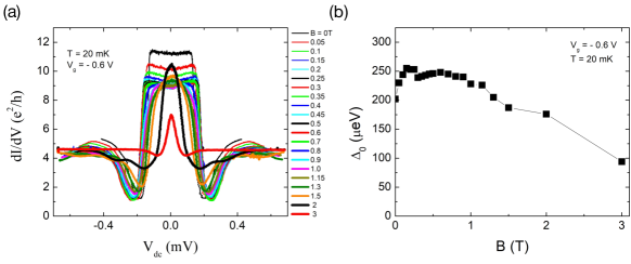
To investigate the edge state regime further, in Fig. 1 (e) we compare three-terminal conductance measurements across the Ta constriction at the gate voltage corresponding to the peak in Rxx ( V) and in the hole-doped regime ( V). Both regimes show a nearly constant conductance before the onset of conductance dips at mV. Figure 2 (a) shows the differential conductance at V for various out-of-plane magnetic fields. It is clear that edge state transport appears to be robust to magnetic fields up to T. Indeed, at 2 T, the zero-bias conductance is still robust despite a Zeeman splitting meV (assuming ) which is almost half of the theoretical bulk gap of InAs/GaSb at .
Dips in the differential conductance at mV are consistent with the superconducting gap of Ta ( eV). This is in contrast with past experiments on superconducting edge states in InAs/GaSb bilayers 40, 39 where the induced gap was noticeably smaller than the parent gap. In Fig. 2 (b) we present the dependence of the gap extracted from the minima of , , as a function of . Firstly, we observe a slight enhancement of both gaps at low fields, similar to past measurements of the gap 39. This may be associated with the strong spin-orbit interaction 42 in the InAs/GaSb bilayer, but the exact microscopic mechanism is unclear. Notably, is nearly constant at low fields and is gradually suppressed by the magnetic field.
Numerical Conductance Simulations
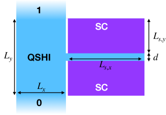
To interpret our measurements, we simulate the electronic transport numerically with a three-terminal setup. Within the bulk gap of a QSHI, nominally we expect a pair of counter-propagating helical edge states to be responsible for charge transport. When one of these edge states encounters a superconducting interface with an excitation energy below the superconducting gap, the process of Andreev reflection occurs where a hole is retroreflected from the superconductor and a pair of electrons co-tunnels into the condensate of Cooper pairs in the superconductor. Perfect Andreev reflection is expected since single electron tunneling into the superconductor and backscattering along the QSHI vacuum edge are forbidden. In our device with a superconducting constriction, however, the geometry of the constriction can strongly affect the probability of Andreev reflection since backscattering and electron tunneling across the constriction edge are allowed. We model this by calculating the scattering matrix coefficients using the python package Kwant 43. First, we treat the superconducting constriction as two parallel superconducting electrodes separated by a small gap (Fig. 1 (a)). We can treat the QSHI-SC system within the BdG formalism as
| (1) |
which satisfies the BdG equation and where the mean-field superconducting gap in the bottom superconducting QPC arm and in the top arm, is the chemical potential, and is the momentum. is the time-reversal operator with complex conjugate operator . The BHZ model describing the QSHI is where is the conventional BHZ model, is the Zeeman spin splitting, describes broken inversion symmetry in the double quantum well 44, , are Pauli matrices in orbital and spin space, respectively. A detailed description of the system is presented in the SM. The dispersion of the BHZ model is shown in Fig. 3 (a) where the linearly crossing bands at are the helical edge states.

To make the connection to our measured conductance in Fig. 2 (a), we calculate the sub-gap conductance of the four-terminal Hall bar shown in the inset of Fig. 3 (a) using a modified Landauer-Büttiker model for helical edge modes. If we consider the possibility of spin-flip processes, then both backscattering of edge states and crossed Andreev reflection may occur in the device, so we include all of these processes in the model. We assume leads 2 and 3 are floating and lead 4 is a grounded superconductor. The Landauer-Büttiker equation for the current in lead is where is the chemical potential of lead , , and with the resistance quantum . Here, . We suppose the currents . We can calculate the resistance
| (2) |
where is the Andreev reflection probability, is the crossed Andreev reflection probability, and is the backscattering probability. The conservation of quasiparticle current is expressed as . Details of this calculation are provided in the SM. At zero magnetic field, we find that assuming a perfect Andreev reflection () and no backscattering and cross Andreev reflection (), the conductance is quantized: , and agrees excellently with experimental observations.
We now present simulations corresponding to finite voltage bias measurements, still at zero field. Details about the simulation are presented in the SM. Using , we show as a function of in Fig. 3 (b) for different constriction widths . When is large, a small mass gap in the constriction suppresses backscattering and leads to a strong Andreev response. As the constriction is narrowed, the Andreev reflection is weakened. This is qualitatively similar to the effect of a potential barrier on Andreev reflection in the BTK model of a normal metal-SC junction. Additionally, we find Andreev reflection associated with the superconducting constriction is robust to Anderson disorder. Figure 3 (c) shows in the presence of Anderson disorder (black line) with a potential amplitude averaged over 55 disorder realizations. In Fig. 3 (c) we compare the experimental conductance at V to the disorder-averaged conductance and find excellent quantitative agreement. We observe only slight deviations near the gap edge, most likely due to non-equilibrium effects and thermal broadening that are not captured in the Landauer-Büttiker description. Importantly, the nearly quantized three-terminal conductance we measured substantiates the existence of helical edge state transport in the device since trivial edge states or bulk carriers lack topological protection, generally leading to a non-quantized conductance that is sensitive to the voltage bias.
A quantized Hall conductance anomalously robust under large magnetic fields has been reported in other InAs/GaSb double quantum wells for in-plane fields as large as 12 T 41. This is in contrast with the general expectation that under a strong B field broken TRS should open a gap at the Dirac point of linearly dispersing edge states, eventually leading to the suppression of edge conductance. A very likely scenario to resolve this discrepancy is one in which the Dirac point is moved down in energy (buried) due to higher-order corrections to the band structure of QSHIs 34, 35. We expect that this to be the case for our devices. Recent work theoretically investigated the impact of a buried Dirac point on Majorana zero modes 45, but study of MKPs in a similar vein is lacking. In the following, we will examine this case.
Majorana Kramer pairs with buried Dirac points
To investigate MKPs with and without a buried Dirac point, we consider a more detailed Hamiltonian for a similar inverted type-II InAs/GaSb bilayer derived from calculations using the Löwdin partitioning technique 35. This effective Hamiltonian is a variation of the BHZ model with additional spin-orbit coupling and momentum terms: (see SM for details). The Hamiltonian allows us to accurately model the two dimensional electron gas in the double quantum well without having to use two different Hamiltonians for the the InAs and GaSb layer and take into account the band-bending effects at the interface between the two layers 46. To compare the properties of MKPs with and without a buried Dirac point as directly as possible, we will consider two Hamiltonians: and where has an exposed Dirac point and has a buried one. includes the term in order to account for structural asymmetries 44 that give rise to a gap opening with the activation of a Zeeman field in the z-direction. In our simulations, we use experimentally relevant parameters nm, nm, and a uniform spatial grid with resolution nm; for more details and the specific parameters of the Löwdin effective model, see SM.
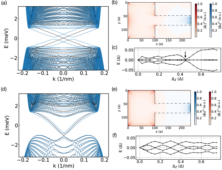
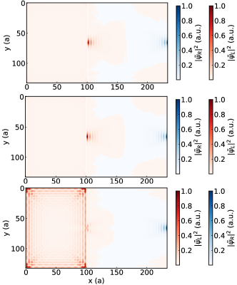
Figure 4 (a) presents the dispersion for with and . To visualize the MKPs, we consider the local density of states of a pair of MKP eigenstates transformed into left- and right-parity states , where are one pair of positive and negative energy MKP eigenstates. This is a useful transformation of both Majorana zero modes and Kramer pairs since the left- and right-parity states are expected to be highly localized with little overlap between them. To be able to visualize using only positive effective weights the spatial profiles of the MKPs, relative to their overlap:
| (3) |
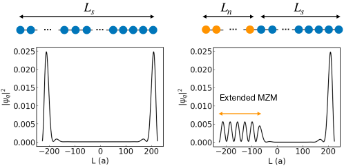
Note that in the thermodynamic limit (), . In Fig. 4 (b) we plot the MKP relative weights with . Compared to Fig. 1 (a), here is extended along the vacuum edge of the QSHI region. This occurs because the tunneling barrier (combination of edge state mass gap and constriction length separating the QPC and QSHI) between the MKP and fermionic modes in the QSHI region is insufficient to pin the left Majorana modes to the constriction. The evolution of MKP energies with Zeeman splitting is presented in Fig. 4 (c). With time-reversal symmetry lifted, the MKPs split from and modulate weakly before evolving near into one pair of Majorana zero modes and a pair of trivial finite energy states.
Before analyzing the viability of MKPs with a buried Dirac point, let’s discuss the impact of the constriction on edge states with an exposed Dirac point compared to a buried one. When top and bottom edge states hybridize in a normal constriction, they open a gap in the dispersion near the Dirac points. When the Dirac point is in the middle of the bulk gap, this can gap out the edge state dispersion if the constriction width is smaller than the penetration of the edge states into the bulk. For edge states with a buried Dirac point, unless exceeds the difference in energy between the Dirac point and the top of the valence band, edge states in the QPC remain gapless regardless of the position of the Fermi energy in the bulk gap. Thus, the key difference arises in the role of the mass gap opening at the Dirac point when the edge states encounter the constriction. Despite this modification to the bands, with a buried Dirac point there still exists two Fermi points with that have superconducting gaps of differing signs inside the phase-biased SC constriction. Then, in principle, pairing of counter-propagating edge states on the top and bottom of the constriction is unaffected by a buried Dirac point, permitting MKPs at the ends of the constriction. Now, in the case of a buried Dirac point where the edge dispersion remains gapless in the constriction, no insulating domain wall exists between the QSHI and SC constriction that pins the MKP. Without a domain wall to pin the MKP, the tunneling between low energy fermionic modes in the QSHI and the MKP can be significant, leading to an extended MKP state. This is similar to what happens to a Majorana zero mode at the end a topological superconductor (TSC) nanowire when it couples strongly to a normal region where the SC gap is removed (see SM). This can also occur with an exposed Dirac point (c.f. Fig. 4 (b)), but it will be ubiquitous with a buried Dirac point.
Figure 4 (d) shows the dispersion of where the Dirac point lies just below the valence band edge for and . In Fig. 4 (e), we present the analog of panel (b) with . The MKP weights are similar to the exposed Dirac point scenario in panel (b), but here the MKP is more localized along the vacuum edge of the QSHI region. In Fig. 4 (f), we notice a qualitative difference in the effect of the Zeeman splitting: oscillations in the MKP energies are regular and persist throughout the range of Zeeman splittings we consider. These oscillations are similar to the oscillations expected in finite-sized systems hosting Majorana zero modes which have been investigated extensively 47, 48, but here they correspond to MKPs rather than a single pair of Majorana zero modes. Importantly, contrary to the case in panel (c) with an exposed Dirac point, in panel (f) no transition occurs to a spinless p-wave state (with a single pair of zero energy states) when the Dirac point is buried. In fact, the MKP weights at finite (see SM) suggest the system still contains weakly hybridized MKPs despite lacking topological protection 49, even for values of where the system is driven into a spinless p-wave phase. This delay in transitioning to a spinless p-wave state can be traced back directly to the buried Dirac point. For Majorana zero modes with buried Dirac points, it was shown that the transition from a trivial phase to a TSC induced by a Zeeman splitting is shifted to larger values of when the chemical potential does not coincide with the Dirac point 45. In our context, the transition from weakly hybridized MKPs to Majorana zero modes is shifted to larger when the chemical potential does not align with the Dirac point. Thus, a buried Dirac point may help preserve the Majorana Kramer pairs under finite magnetic fields.
Summary
To conclude, we fabricated a device based on a InAs/GaSb (15nm/5nm) bilayer with a superconducting Ta constriction. Using an electrostatic gate, we tuned the InAs/GaSb bilayer to a bulk band gap and measured a three-terminal conductance which remained robust up to an external magnetic field of 2 T. Using a modified Landauer-Büttiker analysis accounting for helical edge states and Andreev processes, we found the measured consistent with Andreev reflection probability which is in quantitative agreement with tight binding simulations of the device. The robustness of the conductance to B strongly points to a buried Dirac point. Our simulations show a buried Dirac point in this scheme works to preserve MKPs under broken TRS.
We have shown that a buried Dirac point also reduces the tunneling barrier between the QSHI and the SC constriction, which can cause
any resonant structure associated with the MKPs, such as crossed Andreev reflection 32, 33,
to be washed out. This low tunneling barrier consequentially unpins a MKP (the left side of the constriction in Fig. 4 (b,e)), resulting in a non-local MKP that remains decoupled from the other MKP. Since the coupling of MKPs on either end of the constriction is unaffected, the topological gap is unaffected.
Given that, the MKP can become an extended edge state rather than a localized “defect” and we can apply edge state techniques such as scattering at normal QPCs to probe the MKPs. On the other hand, if we want to pin the MKP as originally proposed, this can be achieved by reducing the separation of the Ta electrodes further to less than 100 nm (see SM), well within the resolution of available lithographic techniques.
References
- Hasan and Kane 2010 M. Z. Hasan and C. L. Kane, Colloquium: Topological insulators, Rev. Mod. Phys. 82, 3045 (2010).
- Qi and Zhang 2011 X.-L. Qi and S.-C. Zhang, Topological insulators and superconductors, Rev. Mod. Phys. 83, 1057 (2011).
- Kane and Mele 2005 C. L. Kane and E. J. Mele, topological order and the quantum spin hall effect, Phys. Rev. Lett. 95, 146802 (2005).
- Bernevig et al. 2006 B. A. Bernevig, T. L. Hughes, and S.-C. Zhang, Quantum spin hall effect and topological phase transition in hgte quantum wells, Science 314, 1757 (2006), https://www.science.org/doi/pdf/10.1126/science.1133734 .
- Fu and Kane 2008 L. Fu and C. L. Kane, Superconducting proximity effect and majorana fermions at the surface of a topological insulator, Phys. Rev. Lett. 100, 096407 (2008).
- Fu and Kane 2009 L. Fu and C. L. Kane, Josephson current and noise at a superconductor/quantum-spin-hall-insulator/superconductor junction, Phys. Rev. B 79, 161408 (2009).
- Tanaka et al. 2009 Y. Tanaka, T. Yokoyama, and N. Nagaosa, Manipulation of the majorana fermion, andreev reflection, and josephson current on topological insulators, Phys. Rev. Lett. 103, 107002 (2009).
- Mong et al. 2014 R. S. K. Mong, D. J. Clarke, J. Alicea, N. H. Lindner, P. Fendley, C. Nayak, Y. Oreg, A. Stern, E. Berg, K. Shtengel, and M. P. A. Fisher, Universal topological quantum computation from a superconductor-abelian quantum hall heterostructure, Phys. Rev. X 4, 011036 (2014).
- San-Jose et al. 2015 P. San-Jose, J. L. Lado, R. Aguado, F. Guinea, and J. Fernández-Rossier, Majorana zero modes in graphene, Phys. Rev. X 5, 041042 (2015).
- Lee et al. 2017 G.-H. Lee, K.-F. Huang, D. K. Efetov, D. S. Wei, S. Hart, T. Taniguchi, K. Watanabe, A. Yacoby, and P. Kim, Inducing superconducting correlation in quantum hall edge states, Nature Physics 13, 693 (2017).
- Zhao et al. 2020 L. Zhao, E. G. Arnault, A. Bondarev, A. Seredinski, T. F. Q. Larson, A. W. Draelos, H. Li, K. Watanabe, T. Taniguchi, F. Amet, H. U. Baranger, and G. Finkelstein, Interference of chiral andreev edge states, Nature Physics 16, 862 (2020).
- Hatefipour et al. 2022 M. Hatefipour, J. J. Cuozzo, J. Kanter, W. M. Strickland, C. R. Allemang, T.-M. Lu, E. Rossi, and J. Shabani, Induced superconducting pairing in integer quantum hall edge states, Nano Letters 22, 6173 (2022), pMID: 35867620.
- Gül et al. 2022 O. Gül, Y. Ronen, S. Y. Lee, H. Shapourian, J. Zauberman, Y. H. Lee, K. Watanabe, T. Taniguchi, A. Vishwanath, A. Yacoby, and P. Kim, Andreev reflection in the fractional quantum hall state, Phys. Rev. X 12, 021057 (2022).
- Cuozzo and Rossi 2024 J. J. Cuozzo and E. Rossi, Su(4) symmetry breaking and induced superconductivity in graphene quantum hall edges, Phys. Rev. B 110, 024518 (2024).
- Hatefipour et al. 2024 M. Hatefipour, J. J. Cuozzo, I. Levy, W. M. Strickland, D. Langone, E. Rossi, and J. Shabani, Andreev reflection of quantum hall states through a quantum point contact, Phys. Rev. B 109, 035430 (2024).
- Kitaev 2001 A. Y. Kitaev, Unpaired majorana fermions in quantum wires, Physics-Uspekhi 44, 131 (2001).
- Nayak et al. 2008 C. Nayak, S. H. Simon, A. Stern, M. Freedman, and S. Das Sarma, Non-Abelian anyons and topological quantum computation, Reviews of Modern Physics 10.1103/RevModPhys.80.1083 (2008), arXiv:0707.1889 .
- Alicea 2012 J. Alicea, New directions in the pursuit of majorana fermions in solid state systems, Reports on Progress in Physics 75, 076501 (2012).
- Lee et al. 2012 E. J. H. Lee, X. Jiang, R. Aguado, G. Katsaros, C. M. Lieber, and S. De Franceschi, Zero-bias anomaly in a nanowire quantum dot coupled to superconductors, Phys. Rev. Lett. 109, 186802 (2012).
- Kells et al. 2012 G. Kells, D. Meidan, and P. W. Brouwer, Near-zero-energy end states in topologically trivial spin-orbit coupled superconducting nanowires with a smooth confinement, Phys. Rev. B 86, 100503 (2012).
- Reeg et al. 2018 C. Reeg, O. Dmytruk, D. Chevallier, D. Loss, and J. Klinovaja, Zero-energy andreev bound states from quantum dots in proximitized rashba nanowires, Phys. Rev. B 98, 245407 (2018).
- Vuik et al. 2019 A. Vuik, B. Nijholt, A. R. Akhmerov, and M. Wimmer, Reproducing topological properties with quasi-Majorana states, SciPost Phys. 7, 061 (2019).
- Liu et al. 2019 C.-X. Liu, J. D. Sau, T. D. Stanescu, and S. Das Sarma, Conductance smearing and anisotropic suppression of induced superconductivity in a majorana nanowire, Phys. Rev. B 99, 024510 (2019).
- Chen et al. 2019 J. Chen, B. D. Woods, P. Yu, M. Hocevar, D. Car, S. R. Plissard, E. P. A. M. Bakkers, T. D. Stanescu, and S. M. Frolov, Ubiquitous non-majorana zero-bias conductance peaks in nanowire devices, Phys. Rev. Lett. 123, 107703 (2019).
- Awoga et al. 2019 O. A. Awoga, J. Cayao, and A. M. Black-Schaffer, Supercurrent detection of topologically trivial zero-energy states in nanowire junctions, Phys. Rev. Lett. 123, 117001 (2019).
- Woods et al. 2019 B. D. Woods, J. Chen, S. M. Frolov, and T. D. Stanescu, Zero-energy pinning of topologically trivial bound states in multiband semiconductor-superconductor nanowires, Phys. Rev. B 100, 125407 (2019).
- Valentini et al. 2021 M. Valentini, F. Peñaranda, A. Hofmann, M. Brauns, R. Hauschild, P. Krogstrup, P. San-Jose, E. Prada, R. Aguado, and G. Katsaros, Nontopological zero-bias peaks in full-shell nanowires induced by flux-tunable andreev states, Science 373, 82 (2021), https://www.science.org/doi/pdf/10.1126/science.abf1513 .
- Hess et al. 2021 R. Hess, H. F. Legg, D. Loss, and J. Klinovaja, Local and nonlocal quantum transport due to andreev bound states in finite rashba nanowires with superconducting and normal sections, Phys. Rev. B 104, 075405 (2021).
- Aghaee et al. 2023 M. Aghaee, A. Akkala, Z. Alam, R. Ali, A. Alcaraz Ramirez, M. Andrzejczuk, A. E. Antipov, P. Aseev, M. Astafev, B. Bauer, J. Becker, S. Boddapati, F. Boekhout, J. Bommer, T. Bosma, L. Bourdet, S. Boutin, P. Caroff, L. Casparis, M. Cassidy, S. Chatoor, A. W. Christensen, N. Clay, W. S. Cole, F. Corsetti, A. Cui, P. Dalampiras, A. Dokania, G. de Lange, M. de Moor, J. C. Estrada Saldaña, S. Fallahi, Z. H. Fathabad, J. Gamble, G. Gardner, D. Govender, F. Griggio, R. Grigoryan, S. Gronin, J. Gukelberger, E. B. Hansen, S. Heedt, J. Herranz Zamorano, S. Ho, U. L. Holgaard, H. Ingerslev, L. Johansson, J. Jones, R. Kallaher, F. Karimi, T. Karzig, E. King, M. E. Kloster, C. Knapp, D. Kocon, J. Koski, P. Kostamo, P. Krogstrup, M. Kumar, T. Laeven, T. Larsen, K. Li, T. Lindemann, J. Love, R. Lutchyn, M. H. Madsen, M. Manfra, S. Markussen, E. Martinez, R. McNeil, E. Memisevic, T. Morgan, A. Mullally, C. Nayak, J. Nielsen, W. H. P. Nielsen, B. Nijholt, A. Nurmohamed, E. O’Farrell, K. Otani, S. Pauka, K. Petersson, L. Petit, D. I. Pikulin, F. Preiss, M. Quintero-Perez, M. Rajpalke, K. Rasmussen, D. Razmadze, O. Reentila, D. Reilly, R. Rouse, I. Sadovskyy, L. Sainiemi, S. Schreppler, V. Sidorkin, A. Singh, S. Singh, S. Sinha, P. Sohr, T. c. v. Stankevič, L. Stek, H. Suominen, J. Suter, V. Svidenko, S. Teicher, M. Temuerhan, N. Thiyagarajah, R. Tholapi, M. Thomas, E. Toomey, S. Upadhyay, I. Urban, S. Vaitiekėnas, K. Van Hoogdalem, D. Van Woerkom, D. V. Viazmitinov, D. Vogel, S. Waddy, J. Watson, J. Weston, G. W. Winkler, C. K. Yang, S. Yau, D. Yi, E. Yucelen, A. Webster, R. Zeisel, and R. Zhao (Microsoft Quantum), Inas-al hybrid devices passing the topological gap protocol, Phys. Rev. B 107, 245423 (2023).
- Teo and Kane 2010 J. C. Y. Teo and C. L. Kane, Topological defects and gapless modes in insulators and superconductors, Phys. Rev. B 82, 115120 (2010).
- Schrade and Fu 2022 C. Schrade and L. Fu, Quantum computing with majorana kramers pairs, Phys. Rev. Lett. 129, 227002 (2022).
- Li et al. 2016 J. Li, W. Pan, B. A. Bernevig, and R. M. Lutchyn, Detection of majorana kramers pairs using a quantum point contact, Phys. Rev. Lett. 117, 046804 (2016).
- Pikulin et al. 2016 D. I. Pikulin, Y. Komijani, and I. Affleck, Luttinger liquid in contact with a kramers pair of majorana bound states, Phys. Rev. B 93, 205430 (2016).
- Li et al. 2018 C.-A. Li, S.-B. Zhang, and S.-Q. Shen, Hidden edge dirac point and robust quantum edge transport in inas/gasb quantum wells, Phys. Rev. B 97, 045420 (2018).
- Skolasinski et al. 2018 R. Skolasinski, D. I. Pikulin, J. Alicea, and M. Wimmer, Robust helical edge transport in quantum spin hall quantum wells, Phys. Rev. B 98, 201404 (2018).
- Yu et al. 2018 W. Yu, V. Clerico, C. H. Fuentevilla, X. Shi, Y. Jiang, D. Saha, W. K. Lou, K. Chang, D. H. Huang, G. Gumbs, D. Smirnov, C. J. Stanton, Z. Jiang, V. Bellani, Y. Meziani, E. Diez, W. Pan, S. D. Hawkins, and J. F. Klem, Anomalously large resistance at the charge neutrality point in a zero-gap inas/gasb bilayer, New Journal of Physics 20, 053062 (2018).
- Yang et al. 1996 M. J. Yang, F. Wang, C. H. Yang, B. R. Bennett, and T. Q. Do, A composite quantum well field-effect transistor, Applied Physics Letters 69, 85 (1996), https://pubs.aip.org/aip/apl/article-pdf/69/1/85/18520026/85_1_online.pdf .
- Yu et al. 2014 W. Yu, Y. Jiang, C. Huan, X. Chen, Z. Jiang, S. D. Hawkins, J. F. Klem, and W. Pan, Superconducting proximity effect in inverted InAs/GaSb quantum well structures with Ta electrodes, Applied Physics Letters 105, 192107 (2014), https://pubs.aip.org/aip/apl/article-pdf/doi/10.1063/1.4901965/13803024/192107_1_online.pdf .
- Shi et al. 2015 X. Shi, W. Yu, Z. Jiang, B. Andrei Bernevig, W. Pan, S. D. Hawkins, and J. F. Klem, Giant supercurrent states in a superconductor-InAs/GaSb-superconductor junction, Journal of Applied Physics 118, 133905 (2015), https://pubs.aip.org/aip/jap/article-pdf/doi/10.1063/1.4932644/15168367/133905_1_online.pdf .
- Pribiag et al. 2015 V. S. Pribiag, A. J. A. Beukman, F. Qu, M. C. Cassidy, C. Charpentier, W. Wegscheider, and L. P. Kouwenhoven, Edge-mode superconductivity in a two-dimensional topological insulator, Nature Nanotechnology 10, 593 (2015).
- Du et al. 2015 L. Du, I. Knez, G. Sullivan, and R.-R. Du, Robust helical edge transport in gated bilayers, Phys. Rev. Lett. 114, 096802 (2015).
- Jeffrey Gardner et al. 2011 H. Jeffrey Gardner, A. Kumar, L. Yu, P. Xiong, M. P. Warusawithana, L. Wang, O. Vafek, and D. G. Schlom, Enhancement of superconductivity by a parallel magnetic field in two-dimensional superconductors, Nature Physics 7, 895 (2011).
- Groth et al. 2014 C. W. Groth, M. Wimmer, A. R. Akhmerov, and X. Waintal, Kwant: A software package for quantum transport, New Journal of Physics 10.1088/1367-2630/16/6/063065 (2014), arXiv:1309.2926 .
- Liu et al. 2008 C. Liu, T. L. Hughes, X.-L. Qi, K. Wang, and S.-C. Zhang, Quantum spin hall effect in inverted type-ii semiconductors, Phys. Rev. Lett. 100, 236601 (2008).
- Schulz et al. 2020 F. Schulz, K. Plekhanov, D. Loss, and J. Klinovaja, Majorana bound states in topological insulators with hidden dirac points, Phys. Rev. Res. 2, 033215 (2020).
- Liu and Allen 1995 Y. Liu and R. E. Allen, Electronic structure of the semimetals bi and sb, Phys. Rev. B 52, 1566 (1995).
- Fleckenstein et al. 2018 C. Fleckenstein, F. Domínguez, N. Traverso Ziani, and B. Trauzettel, Decaying spectral oscillations in a majorana wire with finite coherence length, Phys. Rev. B 97, 155425 (2018).
- Cao et al. 2019 Z. Cao, H. Zhang, H.-F. Lü, W.-X. He, H.-Z. Lu, and X. C. Xie, Decays of majorana or andreev oscillations induced by steplike spin-orbit coupling, Phys. Rev. Lett. 122, 147701 (2019).
- Zhang et al. 2013 F. Zhang, C. L. Kane, and E. J. Mele, Time-reversal-invariant topological superconductivity and majorana kramers pairs, Phys. Rev. Lett. 111, 056402 (2013).
Acknowledgements
J.J.C. acknowledges helpful discussions with Rafal Skolasinski. J.C.C. is supported by a LDRD project.
Work by E.R. and W.P. was funded by the US Department of Energy, Office of Basic Energy Sciences, via Award DE-SC0022245.
Materials growth was supported by the LDRD program at Sandia. Device fabrication was carried out at CINT, a user facility by DOE.
Sandia National Laboratories is a multi-mission laboratory managed and operated by National Technology & Engineering Solutions of Sandia, LLC (NTESS), a wholly owned subsidiary of Honeywell International Inc., for the U.S. Department of Energy’s National Nuclear Security Administration (DOE/NNSA) under contract DE-NA0003525. This written work is authored by an employee of NTESS. The employee, not NTESS, owns the right, title and interest in and to the written work and is responsible for its contents. Any subjective views or opinions that might be expressed in the written work do not necessarily represent the views of the U.S. Government. The publisher acknowledges that the U.S. Government retains a non-exclusive, paid-up, irrevocable, world-wide license to publish or reproduce the published form of this written work or allow others to do so, for U.S. Government purposes. The DOE will provide public access to results of federally sponsored research in accordance with the DOE Public Access Plan.
Author contributions
W.P. conceived the experiment. W.Y., X.S., A.J.M, S.D.H., J.F.K., and W.P. contributed to experimental investigations. J.J.C., W.P. and E.R. analyzed the transport data. J.J.C. and E.R. developed the theoretical model and performed the numerical simulations. J.J.C., W.P. and E.R. wrote the manuscript with inputs from all authors.
Competing interests
The authors declare no competing interests.
Data and materials availability
All data are available from the corresponding authors upon request.
SUPPLEMENTAL MATERIAL
I Additional Experimental Data
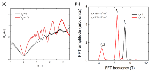
Magnetoresistance () data in the device region without the superconductor is shown in Fig. S1. At both = 0 and -1 V, the Shubnikov-de Haas oscillations are observed (Fig. S1a). Fast Fourier Transform (FFT) analysis of these SdH oscillations is carried out, from which the electron density = 3.851011 cm-2 at = 0V and hole density = 3.151011 cm-2 at = -1V are deduced. Furthermore, their mobilities are obtained. At = 0 V, = 8.1×104 cm2/Vs; at = -1 V, = 9.4104 cm2/Vs. The calculated electron and hole mean free path is 0.83 m and 0.87 m, respectively. These mean free paths are smaller than the device dimension (3 m). So, bulk contribution to is large. This explains why the peak conductance at V is much larger than 2 (expected for pure edge transport).
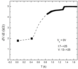
In Fig. S2, we present three-terminal differential resistance dV/dI at = 0 V measured as a function of sample temperature (T). It is constant at high temperatures. The sharp drop at T 1.3 K is due to the onset of the superconducting transition of the Ta electrode. dV/dI continues decreasing as the temperature is lowered.
II BHZ Tight Binding Model
To simulate the conductance across the SPC, we use the following tight binding Bogoliubov-de Gennes Hamiltonian on a square lattice:
| (S1) |
where () is the creation (annihilation) operator for an electron at site in orbital with spin , and , and are Pauli matrices. is the chemical potential, assumed to be uniform throughout the system. The superconducting gap is taken to be in the top superconductor, in the bottom superconductor, and zero otherwise. Due to the bulk and structural inversion asymmetries in the double quantum well, we include the term
| (S2) |
where , and describe the bulk inversion asymmetry and describes the structural inversion asymmetry. The dimensions of the system modeled are shown in Fig. S3.
| 0.5 | 0.05 | 1 | 0.6 | 0.3 | 0.01 | 0.06 | 0.003 | 0.003 | 80 | 140 | 100 | 40 |
III Löwdin effective Tight Binding Model
We model the buried Dirac point in InAs/GaSb using the effective Hamiltonian derived in Ref. 35:
| (S3) |
where, using abbreviated notation for Kronecker products, we have
| (S4) | ||||
| (S5) | ||||
| (S6) | ||||
| (S7) |
and with . The matrices and are Pauli matrices in Nambu, spin, and orbital spaces, respectively, with and .
| Hamiltonian | |||||||||||||||||
|---|---|---|---|---|---|---|---|---|---|---|---|---|---|---|---|---|---|
| 108 | 0.8 | -6.2 | -273.4 | 98.4 | -116.5 | 3.4 | 10.1 | 0 | 6.5 | -8.95 | -18.5 | 0 | -35.8 | -0.16 | 6.73 | 3.0 | |
| 108 | 0.8 | -6.2 | -273.4 | 98.4 | -116.5 | 32.8 | 96.4 | -170.2 | 62.5 | -85.5 | -18.5 | 179.4 | -341.9 | -1.6 | 64.3 | 3.0 |
IV Conductance calculations
In the four-terminal setup presented in the main text, we assume contact 4 is a grounded superconductor. Then we can generalize the LB method to account for Andreev processes 12:
| (S8) |
where is the voltage of the superconducting lead and
| (S9) |
where is the electron transmission from lead to lead , is the transmission of an electron from lead to a hole in lead (i.e. Andreev reflection), and
| (S10) |
is the total number of modes in lead .
We assume the energy of electrons injected from normal contacts is below the superconducting gap so that the current in lead 4 is entirely due to Andreev reflection. Furthermore, we assume helical edge states are the only allowed modes in the system i.e. ignore bulk contributions.
Time-reversal symmetry gives us
| (S11) | ||||
| (S12) |
where , and quasiparticle number conservation gives us
| (S13) |
Then we can derive the conductance matrix for the Hall bar by expressing each current in terms of the voltages of the normal contacts. For contact 1
| (S14) | ||||
| (S15) | ||||
| (S16) |
Similarly
| (S17) | ||||
| (S18) |
Then the conductance can be found by solving the matrix equation
| (S19) |
where
V Additional Simulation Data
