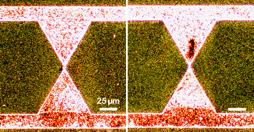
Visual and quantitative analysis of the trapping volume
in dielectrophoresis of nanoparticles
Abstract
Nanoparticle manipulations require a careful analysis of the forces at play. Unfortunately, traditional force measurement techniques based on the particle velocity do not provide a sufficient resolution, while balancing approaches involving counteracting forces are often cumbersome. Here, we demonstrate that a nanoparticle dielectrophoretic response can be quantitatively studied by a straightforward visual delineation of the dielectrophoretic trapping volume. We reveal this volume by detecting the width of the region depleted of gold nanoparticles by the dielectrophoretic force. Comparison of the measured widths for various nanoparticle sizes with numerical simulations obtained by solving the particle–conservation equation shows excellent agreement, thus providing access to the particles physical properties, such as polarizability and size. These findings can be further extended to investigate various types of nano–objects including bio– and molecular aggregates and offer a robust characterization tool that can enhance the control of matter at the nanoscale.
Electrokinetic effects enable the precise and long–range control of the position of numerous micro- and nanoscale species. As such, they have tremendous potential for both fundamental [1, 2, 3, 4] and applied research [5, 6, 7]. For example, dielectrophoresis (DEP) can renovate the field of separation techniques [8, 9]. Indeed, there is a solid body of research that features the successful utilization of the DEP force for transport [10], trapping [11, 12], separation [13, 14, 15], and concentration [16, 17, 18, 19] of different inorganic and biological substances. However, a reliable DEP experiment requires a valid experimental estimate of the DEP force, which is usually not straightforward. There is no possibility to measure the DEP force directly and it is typically estimated indirectly, which is possible only as long as a precise theoretical model for DEP exists; unfortunately this may not always be the case, e.g. for submicron bioparticles [20, 21, 22, 23, 24, 25]. Therefore, developing new force measurement strategies is of fundamental interest for DEP research and its application in nanosciences.
Several approaches have been proposed to measure the DEP force [26]. The most common one relies on estimating the particle velocity from videos recorded on an optical microscope [27, 28, 29, 30]. The DEP force can then be determined by solving the Langevin equation [31, 32]. However, a reliable force estimate obtained this way also requires the correct definition of all the other forces that may act on the particle during DEP. Furthermore, if the particles are unlabeled and in low concentration, this method is unsuitable for nanoscale particulates, simply because their observation in an optical microscope is challenging. Alternatively, the DEP force can be measured by a balancing approach that requires another counteracting force of known magnitude, such that the total force on the target object vanishes. For example, the counteracting force can be optical [33, 34, 35], gravity [36], drag [13, 37, 38], or thermal randomizing caused by the Brownian motion [39]. We recently used the latter with a gradient array of conductive electrodes to measure the DEP polarizability factors for three proteins [39]. Unfortunately, the proposed electrodes cannot be utilized to investigate a negative DEP force and the corresponding protein polarizability because their configuration does not provide clearly defined regions with minimum electric field gradient intensities, where the negative DEP trapping can be detected. Other strategies are also available to measure the DEP force, including measurements of the collection rate [40, 41, 42, 43], cross–over frequency [44, 45, 46], and levitation height [47, 48].
Here, we report a straightforward visual representation and quantitative estimate of a particle DEP response, which relies on revealing the DEP trapping volume. The key advantage of this technique is that it does not require special electrodes design or complicated experimental setups to gain a quantitative description of the particle movement. Rather, it can be applied to any DEP platform to reveal the interplay between different forces acting on the particle during the experiment. Besides, it may be applied to investigate any substance in both negative and positive DEP regimes, thus providing the frequency dependence of the DEP polarizability. Furthermore, it can be used to gain quantitative understanding of the temperature, pH, and conductivity dependencies of the DEP polarizability. All of this can be extremely useful for addressing fundamental challenges in DEP, such as the development and verification of new DEP models for the accurate ab initio simulations of the DEP response of bio–nanoparticles [21, 22, 23, 25].
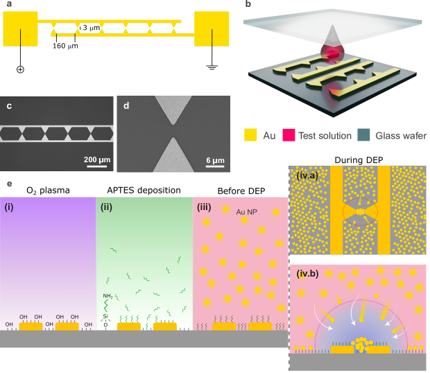
The DEP platform utilized in this work is depicted in Figures 1a–d (see Materials and Methods in the Supporting Information for fabrication details). It consists of periodically repeated sawtooth gold electrode pairs on a glass substrate separated by a fixed gap of 3 m. The lateral distance between sawtooth gaps is 250 m to avoid any coupling between adjacent electrodes. The DEP is readily observed when these electrodes are immersed in an aqueous dispersion of nanoparticles and energized by an external electrical signal. The time-averaged DEP force acting on a nanoparticle in solution is defined as [8, 9]
| (1) |
where R is the particle radius, the dielectric constant of the particle, the medium dielectric constant, the vacuum permittivity, and the amplitude of the electric field. The term in square brackets in Eq. (1) is the real part of the Clausius–Mossotti (CM) or DEP polarizability factor – the most critical and intricate parameter for the accurate description of DEP [20, 21]. It does not only determine the direction of a particle movement in an inhomogeneous electric field but also influences the magnitude of the DEP force [9].
Our hypothesis to experimentally estimate the DEP parameters in Eq. (1) is that two distinct volumes must appear near the electrodes during a DEP trapping experiment, with respectively high and low concentrations of nanoparticles. The volume with a low concentration – also known as the depletion or trapping volume [49, 50, 51, 52] – is where DEP translates nanoparticles towards (positive DEP) or away from (negative DEP) the strongest electric field gradient. This translation occurs because the time-averaged DEP potential energy, , of nanoparticles inside the trapping volume, exceeds the thermal randomizing energy, [1, 53]:
| (2) |
| (3) |
where is Boltzmann’s constant and the absolute temperature.
Figure 1e sketches the measurement procedure of the DEP trapping volume. To test our hypothesis, we use Au nanoparticles of different radii, although the technique is applicable to any substance. The cross–section of the trapping volume is experimentally recorded by analyzing the dark–field scattering from Au nanoparticles immobilized on the DEP device surface. To provide an appropriate contrast between high and low (i.e., depleted by DEP) concentration regions, we also functionalize the device with APTES (Figure 1e, steps (i)–(iii)). In the absence of DEP, APTES ensures a strong binding of nanoparticles to the surface, producing a uniform nanoparticle layer evidenced by a smooth background scattering intensity. This layer slowly builds up everywhere on the surface by the diffusion–limited motion of nanoparticles, Figure 1e(iii). On the other hand, when the electric field is applied to the electrodes and DEP sets in, nanoparticles are rapidly moved by DEP from within the depletion region to the electrode apexes, preventing interaction with APTES. This leads to a local depletion of the number of nanoparticles adsorbed on the surface, which reduces the dark–field scattering intensity from this region, as illustrated in panels (iv.a) and (iv.b) in Figure 1e. The scattering intensity is recorded and analyzed to obtain its spatial profile.
In general, the concentration of Au nanoparticles in DEP experiments evolves as the result of the interplay between nanoparticle drift and subsequent diffusion process caused by their DEP–induced redistribution in space. Assuming an ensemble of non–interacting nanoparticles, this concentration profile is given by the particle–conservation equation [54, 55, 56]:
| (4) |
where is the volume fraction of particles (referred further as the concentration, for brevity) with particle number density and volume , is the velocity of the liquid medium, and is the total flux consisting of the sum of the diffusion, , sedimentation, , and DEP fluxes, :
| (5) |
with
| (6) |
| (7) |
| (8) |
where is the diffusion coefficient for Au nanoparticles, the liquid viscosity, and is the sedimentation force with the medium and the particle densities, and gravitational acceleration [1, 57].
The solution of Eq. (4) provides the spatial–temporal evolution of the nanoparticle concentration, which can be effectively compared with experimental results and used to quantitatively characterize the DEP response of a particle. However, obtaining this solution for specific experimental conditions is not straightforward and requires a careful definition of initial and boundary conditions [55].
In this work, we obtain quantitative information on DEP by comparing the size of the low dark–field intensity measured on the DEP device surface with numerical simulations obtained by solving Eq. (4) assuming stationary conditions, such that the first term on the left–hand side vanishes. This simplification is possible because the experimental conditions are usually long enough to reach equilibrium between the DEP–induced transport and the diffusion of particles. The results obtained by A. Castellanos et al. also suggest that we can neglect the sedimentation flux defined in Eq. (7) because the displacement caused by gravity and buoyancy for particles with a 25–75 nm radius in water is smaller than the displacements induced by DEP and thermal perturbations [57]. Finally, our experimental conditions, including low buffer conductivity (16 S/cm) and an optimized frequency of the applied electric field (3 MHz), suppress the bulk fluid movement upon DEP, and convection, , vanishes. As a result, the solution of Eq. (4) for the nanoparticle concentration on the DEP device surface takes the following form [1, 55]:
| (9) |
where is an arbitrary integration constant. The exponential in Eq. (9) echoes the condition introduced in Eq. (3) and indicates that the boundaries between depleted and undepleted regions are smeared out for an ensemble of nanoparticles due to their random thermal perturbation.
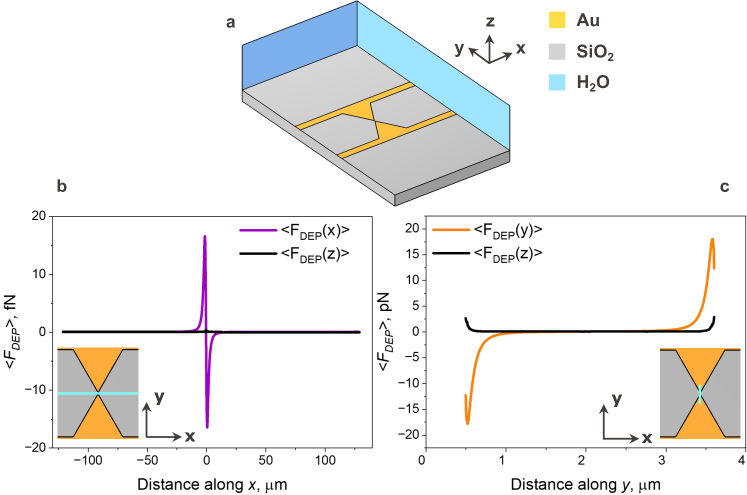
It should also be noted that the argument of the exponential in Eq. (9) is negative because we study the surface concentration of Au nanoparticles, which is assumed to be the inverse of the bulk concentration profile. This approximation is justified for the following reasons. In positive DEP experiments, the bulk particle concentration near electrodes increases progressively with time, reaching the steady–state maximum value in the strongest electric field gradient region (see Figure S1 in the Supporting Information). At the same time, as revealed in our simulations, the perpendicular component of the DEP force, , which is responsible for nanoparticle translation to and adsorption onto the surface, is much weaker compared to the lateral ones, and which induce nanoparticles movement parallel to the surface (see Figure S2 in the Supporting Information). Hence, we can assume that the DEP device surface is depleted in the trapping volume by roughly the same number of nanoparticles as accumulated in the bulk liquid just above the surface.
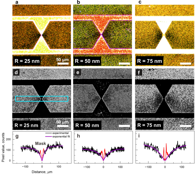
Let us first support the proposed hypothesis and above analysis with experimental results. Figures 2a–c show the dark–field scattering images acquired for Au nanoparticles with different radii after DEP (15 Vp-p and 3 MHz). The regions of high and low dark–field scattering intensities are well visible, with the lowest intensity near the electrode apexes and a progressive intensity increase as one moves away from them. At some distance from the electrode gap, the dark–field intensity reaches a certain magnitude and then remains constant, indicating that one has left the depletion region and entered undepleted space, where the exponential in Eq. (9) becomes negligible. Figure 2 also indicates that this transition is observed farther from the electrode gap for larger nanoparticles, which is also expected from Eq. (9) because the DEP potential energy of nanoparticles has a cubic dependence on their radii. Hence, the obtained scattering profiles can be reliably attributed to the generation of the DEP depletion region.
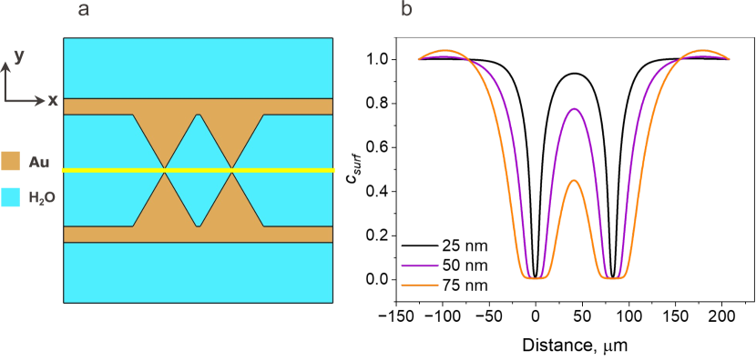
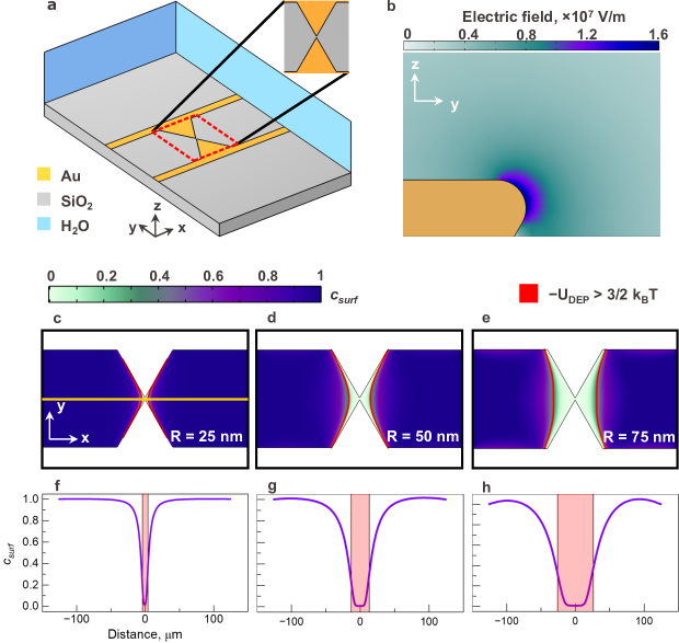
Let us now compare experimental data with simulated concentration profiles. The 3D simulation domain and corresponding electric field intensity distribution near the sawtooth electrode apex are shown in Figure 3a and 3b (see Materials and Methods in the Supporting Information for additional simulation details). This model is based on the effectively fabricated geometry, as shown in Figures 1c,d. The geometrical parameters, including the radii of curvature utilized to simulate the electrode tip apex, were carefully determined using SEM and focused ion beam images [39]. A maximum electric field intensity of V/m was calculated near the electrode apex for an applied peak–to–peak voltage of 15 V.
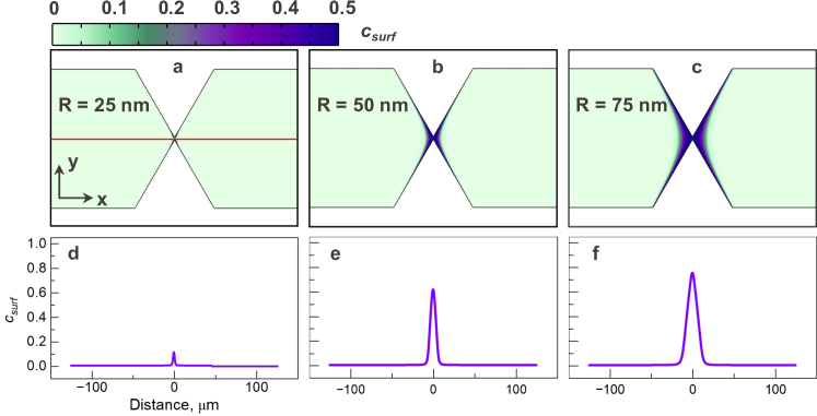
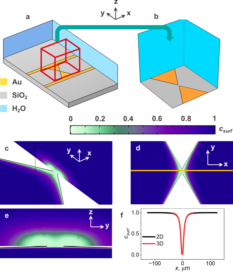
We utilize the electric field components and simulated in 3D to compute in the plane of the DEP device surface, see Eq. (8), and calculate the Au nanoparticle concentration distributions, by solving Eq. (4) in 2D (see Materials and Methods in the Supporting Information for additional simulation details that indicate that the same concentration profiles are observed when Eq. (4) is solved in 3D). The obtained concentration profiles are shown in Figures 3c–h. Figures 3c–e show the spatial variation of the concentration near the electrodes, while Figures 3f–h depict the same concentration profiles along the yellow line in Figure 3c. These figures indicate a significant concentration variation near the electrodes, revealing the shape and size of the depletion regions, which are in a good agreement with the experimental scattering profiles shown in Figure 2a–i. The minimum of surface concentration is observed for all the studied nanoparticles in the middle of the gap between the electrodes. It gradually increases with the distance from the gap, approaching the high concentration limit. Besides, Figures 3c–h indicate that the depletion region is wider for larger Au nanoparticle, which is again in agreement with the scaling of defined by Eq. (2).
| Depletion region size, m | R, nm | ||
|---|---|---|---|
| Au nominal radius, nm | Experimental | Simulated | Calculated by Eq. (S2) |
| 25 | 16.0 4.4 | 9.7 | 30.8 2.9 |
| 50 | 35.6 8.8 | 36.0 | 48.5 7.9 |
| 75 | 61.4 12.4 | 63.7 | 71.1 10.7 |
At this point, we should emphasize the importance of considering nanoparticle diffusion to simulate the depletion region size. This can be observed in Figures 3c–h, where the red contour depicts the spatial extension of the condition in Eq. (3). The width of the depletion region defined by Eq. (3) and calculated along the yellow line in Figure 3c, varies with the nanoparticle radius: 7.6 m, 25.9 m, and respectively 52.4 m for 25 nm, 50 nm, and respectively 75 nm Au nanoparticles. It is noteworthy that the actual width of the surface concentration variation can be significantly larger than that obtained by balancing the thermal energy, especially for small particles sizes (see the concentration value at which the red band crosses the concentration profile for various Au nanoparticle radii in Figure 3f-h). These results indicate that – when investigating the DEP of a nanoparticle ensemble – the trapping volumes must be estimated by applying the laws of statistical physics.
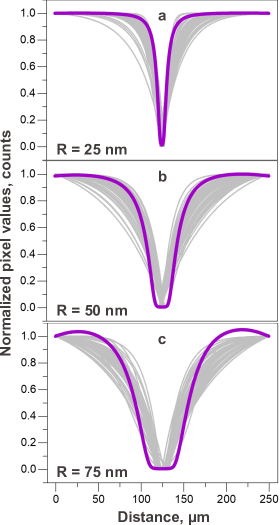
Let us now compare the obtained experimental scattering profiles with the simulated concentration distributions of Au nanoparticles. Figure 4 shows the dark–field scattering intensity fits for approx. 50 various sawtooth microelectrode pairs. The gray curves represent the corresponding concentration profiles for Au nanoparticles with radii of 25 nm (Figure 4a), 50 nm (Figure 4b), and 75 nm (Figure 4c). The purple lines in Figure 4 correspond to the simulated concentration profiles shown in Figure 3f–h. The average experimental sizes of the depletion region after DEP for various nanoparticles are shown in Table 1. These values are in very good agreement with the simulation results.
To demonstrate that the proposed approach can be effectively utilized for the quantitative characterization of the DEP response of different nanoscopic objects, we analyze the obtained concentration profiles and estimate the Au nanoparticle radius (see the Supporting Information for calculation procedure). The calculation results are summarized in the last column of Table 1. The agreement between the experimentally deduced radii and their nominal values is excellent. This approach is very general and can be used to determine any parameter in Eq. (S2), including the DEP polarizability factor.
Let us also note that the accuracy achieved here results from a careful optimization of the experimental conditions. At least two critical factors may lead to significant errors and must be carefully handled for the correct estimation of the depletion region (see the Supporting Information for further discussion). One relates to the first term in brackets in Eq. (4) – the convection – and accounts for mass transfer induced by the bulk fluid movement. In very high conductivity media, the convection magnitude may vastly exceed the DEP force, which complicates the depletion region visualization. The second factor that may obscure the depletion region in experiments is an inappropriate choice of the DEP electrode geometry. Indeed, the electrodes must ensure sufficient space between adjacent DEP traps to prevent the intersection of their depletion regions.
In summary, we have demonstrated that the experimental visualization of the equilibrium between particle diffusion and DEP translation can be utilized to investigate the DEP response of nanoscopic objects. As an example, we chose a colloidal solution of Au nanoparticles with different radii, calculated their trapping volumes from the concentration profiles measured in experiments, and compared the obtained results with numerical simulations. We also utilized these experimental concentration profiles to extract quantitative information on the system under test – here the Au nanoparticle radii. An excellent agreement was found between simulations and experiments, indicating the robustness of the proposed technique, which can be useful to investigate a broad diversity of analytes, for which more sophisticated DEP models are required. These findings shall stimulate experimental efforts to investigate the DEP response of more complex nanoscale particulates and assist the theoretical advancements in this field, rendering DEP a more quantitative and versatile tool for manipulations at the micro– and nanoscales.
Acknowledgements.
The authors thank Christian Santschi and Sergejs Boroviks for fruitful discussions on the experimental and simulation data. This research did not receive any specific funding.References
- Ramos et al. [1998] A. Ramos, H. Morgan, N. G. Green, and A. Castellanos, Journal of Physics D: Applied Physics 31, 2338 (1998).
- Schoch et al. [2008] R. B. Schoch, J. Han, and P. Renaud, Reviews of Modern Physics 80, 839 (2008).
- Squires and Quake [2005] T. M. Squires and S. R. Quake, Reviews of Modern Physics 77, 977 (2005).
- Riccardi and Martin [2023] M. Riccardi and O. J. F. Martin, Chemical Reviews 123, 1680 (2023), publisher: American Chemical Society.
- Yuan et al. [2007] Z. Yuan, A. L. Garcia, G. P. Lopez, and D. N. Petsev, Electrophoresis 28, 595 (2007).
- Llorente et al. [2014] I. Llorente, S. Fajardo, and J. M. Bastidas, Journal of Solid State Electrochemistry 18, 293 (2014).
- Mir et al. [2011] M. Mir, S. Martínez-Rodríguez, O. Castillo-Fernández, A. Homs-Corbera, and J. Samitier, Electrophoresis 32, 811 (2011).
- Pethig [2010] R. Pethig, Biomicrofluidics 4, 022811 (2010), publisher: American Institute of PhysicsAIP.
- Pethig [2017] R. Pethig, Dielectrophoresis: theory, methodology and biological applications (John Wiley & Sons, Hoboken, NJ, 2017) iSSN: 00136654.
- Camacho-Alanis et al. [2012] F. Camacho-Alanis, L. Gan, and A. Ros, Sensors and Actuators, B: Chemical 173, 668 (2012), publisher: Elsevier B.V.
- Hughes and Morgan [1998] M. P. Hughes and H. Morgan, Journal of Physics D: Applied Physics 31, 2205 (1998).
- Hölzel et al. [2005] R. Hölzel, N. Calander, Z. Chiragwandi, M. Willander, and F. F. Bier, Physical Review Letters 95, 18 (2005).
- Liu and Hayes [2021] Y. Liu and M. A. Hayes, Analytical Chemistry (2021), 10.1021/acs.analchem.0c02763.
- Regtmeier et al. [2007] J. Regtmeier, T. T. Duong, R. Eichhorn, D. Anselmetti, and A. Ros, Analytical Chemistry 79, 3925 (2007), publisher: American Chemical Society.
- Yunus et al. [2013] N. A. M. Yunus, H. Nili, and N. G. Green, Electrophoresis 34, 969 (2013).
- Liao and Chou [2012] K. T. Liao and C. F. Chou, Journal of the American Chemical Society 134, 8742 (2012).
- LaLonde et al. [2015] A. LaLonde, M. F. Romero-Creel, M. A. Saucedo-Espinosa, and B. H. Lapizco-Encinas, Biomicrofluidics 9, 064113 (2015).
- D’Amico et al. [2017] L. D’Amico, N. J. Ajami, J. A. Adachi, P. R. Gascoyne, and J. F. Petrosino, Lab on a Chip 17, 1340 (2017).
- Nguyen and Jen [2018] N.-V. Nguyen and C.-P. Jen, Biosensors and Bioelectronics 121, 10 (2018).
- Pethig [2019] R. Pethig, Electrophoresis 40, 2575 (2019).
- Pethig [2022] R. Pethig, Micromachines 13, 261 (2022).
- Hölzel and Pethig [2020] R. Hölzel and R. Pethig, Micromachines 11, 533 (2020).
- Hölzel and Pethig [2021] R. Hölzel and R. Pethig, Electrophoresis 42, 513 (2021).
- Seyedi and Matyushov [2018] S. S. Seyedi and D. V. Matyushov, Journal of Physical Chemistry B 122, 9119 (2018).
- Heyden and Matyushov [2020] M. Heyden and D. V. Matyushov, Journal of Physical Chemistry B 124, 11634 (2020).
- Hoettges [2010] K. F. Hoettges, in Microengineering in Biotechnology, Methods in Molecular Biology, edited by M. P. Hughes and K. F. Hoettges (Humana Press, Totowa, NJ, 2010) pp. 183–198.
- Watarai et al. [1997] H. Watarai, T. Sakamoto, and S. Tsukahara, Langmuir 13, 2417 (1997).
- Huang et al. [1992] Y. Huang, R. Holzel, R. Pethig, and X.-B. Wang, Physics in Medicine & Biology 37, 1499 (1992).
- Kralj et al. [2006] J. G. Kralj, M. T. W. Lis, M. A. Schmidt, and K. F. Jensen, Analytical Chemistry 78, 5019 (2006).
- Ai et al. [2009] Y. Ai, S. W. Joo, Y. Jiang, X. Xuan, and S. Qian, Electrophoresis 30, 2499 (2009).
- Lemons and Gythiel [1997] D. S. Lemons and A. Gythiel, American Journal of Physics 65, 1079 (1997).
- Langevin [1908] P. Langevin, C. R. Acad. Sci. Paris 146, 530 (1908).
- Park et al. [2014] I. S. Park, S. H. Park, D. S. Yoon, S. W. Lee, and B.-M. Kim, Applied Physics Letters 105, 103701 (2014).
- Hong et al. [2010] Y. Hong, J.-W. Pyo, S. H. Baek, S. W. Lee, D. S. Yoon, K. No, and B.-M. Kim, Optics Letters 35, 2493 (2010).
- Jeon et al. [2017] H.-J. Jeon, H. Lee, D. S. Yoon, and B.-M. Kim, Biomedical Engineering Letters 7, 317 (2017).
- Imasato and Yamakawa [2008] H. Imasato and T. Yamakawa, Journal of Electrophoresis 52, 1 (2008).
- Lu et al. [2020] Y.-W. Lu, C. Sun, Y.-C. Kao, C.-L. Hung, and J.-Y. Juang, Nanomaterials 10, 1364 (2020).
- Su et al. [2013] H.-W. Su, J. L. Prieto, and J. Voldman, Lab on a Chip 13, 4109 (2013).
- Zavatski et al. [2023] S. Zavatski, H. Bandarenka, and O. J. F. Martin, Analytical Chemistry 95, 2958 (2023).
- Labeed et al. [2003] F. H. Labeed, H. M. Coley, H. Thomas, and M. P. Hughes, Biophysical Journal 85, 2028 (2003).
- Labeed et al. [2006] F. H. Labeed, H. M. Coley, and M. P. Hughes, Biochimica et Biophysica Acta (BBA) - General Subjects 1760, 922 (2006).
- Markx et al. [1994] G. H. Markx, Y. Huang, X.-F. Zhou, and R. Pethig, Microbiology 140, 585 (1994).
- Hübner et al. [2003] Y. Hübner, K. F. Hoettges, and M. P. Hughes, Journal of Environmental Monitoring 5, 861 (2003).
- Hughes et al. [1998] M. P. Hughes, H. Morgan, F. J. Rixon, J. P. H. Burt, and R. Pethig, Biochimica et Biophysica Acta (BBA) - General Subjects 1425, 119 (1998).
- Green et al. [1997] N. G. Green, H. Morgan, and J. J. Milner, Journal of Biochemical and Biophysical Methods 35, 89 (1997).
- Schnelle et al. [1996] T. Schnelle, T. Müller, S. Fiedler, S. G. Shirley, K. Ludwig, A. Herrmann, G. Fuhr, B. Wagner, and U. Zimmermann, Naturwissenschaften 83, 172 (1996).
- Jones and Bliss [2008] T. B. Jones and G. W. Bliss, Journal of Applied Physics 48, 1412 (2008).
- Kaler and Jones [1990] K. V. Kaler and T. B. Jones, Biophysical Journal 57, 173 (1990).
- Bakewell and Morgan [2006] D. Bakewell and H. Morgan, IEEE Transactions on NanoBioscience 5, 1 (2006).
- Cummings and Singh [2003] E. B. Cummings and A. K. Singh, Analytical Chemistry 75, 4724 (2003).
- Cummings [2003] E. Cummings, IEEE Engineering in Medicine and Biology Magazine 22, 75 (2003).
- Ding et al. [2016] J. Ding, R. M. Lawrence, P. V. Jones, B. G. Hogue, and M. A. Hayes, Analyst 141, 1997 (2016).
- Washizu et al. [1994] M. Washizu, S. Suzuki, O. Kurosawa, T. Nishizaka, and T. Shinohara, IEEE Transactions on Industry Applications 30, 835 (1994).
- Kittel [2004] C. Kittel, Elementary statistical physics, Dover books on physics (Dover Publ, Mineola, NY, 2004).
- Bakewell [2011] D. J. Bakewell, Journal of Physics D: Applied Physics 44, 085501 (2011).
- Loucaides et al. [2011] N. G. Loucaides, A. Ramos, and G. E. Georghiou, Journal of Electrostatics 69, 111 (2011).
- Castellanos et al. [2003] A. Castellanos, A. Ramos, A. González, N. G. Green, and H. Morgan, Journal of Physics D: Applied Physics 36, 2584 (2003).
SUPPORTING INFORMATION
Materials and Methods
Chemicals. (3-Aminopropyl)triethoxysilane (APTES, 99 ), acetone, 2-propanol (IPA, 99.5 ), ethanol (99 ), toluene (anhydrous, 99.8 ), 50 nm, 100 nm, and 150 nm diameter gold nanoparticles (NPs, stabilized suspension in citrate buffer) were purchased from Sigma-Aldrich. 0.22 m syringe filters with polytetrafluorethylen (PTFE) membrane were obtained from Whatman Anotop. 9 mm diameter imaging spacers were acquired from Grace Bio-Labs SecureSeal.
Dielectrophoretic device fabrication. Standard microelectronics techniques were employed for the dielectrophoretic device fabrication [S1, S2], and the detailed procedure is described elsewhere [S3]. Briefly, a 100 mm borosilicate wafer was cleaned in piranha solution and treated in high-frequency oxygen plasma. Standard photolithography procedures, including negative photoresist spin-coating, exposure, and development, were utilized to produce sawtooth microelectrode patterns on a borosilicate wafer. Next, the electron beam evaporation technique was used to deposit 5 nm Ti and 100 nm Au electrode material. Finally, the lift-off step and wafer dicing were conducted to produce 31 x 25 mm2 DEP chips.
Numerical simulations. The finite-elements simulations for the developed DEP device were performed using the AC/DC and Mathematics (classical partial differential equations, stabilized convection-diffusion equation) modules of COMSOL Multiphysics 6.1. The electric field intensity distribution was calculated near sawtooth metal electrodes based on the simulation of the potential distribution by solving the Laplace equation: . The electric field thus was obtained as . Simulations were conducted for a unit cell of one gold sawtooth electrode pair attached to the 20 m wide gold rectangle. The thickness of electrodes and the gap size between sawtooth pairs were 100 nm and 3 m, respectively. Electrodes were located on 250.4 × 585.43 × 30 m3 (width × depth × height) SiO2 substrate and immersed in the water medium of the same width and depth but with 120 m height. One of the electrodes from the pair was grounded, while the boundary condition for the second was , where V, which corresponds to the experimental value of the electric field. The frequency of the electric field was 3 MHz. Periodic boundaries were applied in direction, and electric insulation conditions were for the remaining boundaries. The field was simulated in a water background, assuming a dielectric permittivity = 78 and an electrical conductivity of 16 S/cm. Gold with = 456 kS/cm and = 6.9 was used for the electrode material. The minimum mesh size used for the discretization was 5 nm near the electrode apex. The Au NPs concentration distribution was calculated in 2D in the plane of the DEP device surface by solving the modified particle-conservation equation (see Eq. (4) in the main text) to account for the particle steric effect [S4]. This modification is important to improve the convergence of the simulation results and obtain realistic particle concentrations. No flux boundary conditions were applied anywhere except the left and right boundaries of the simulation domain, for which Dirichlet boundary conditions were introduced, such that the particle volume fraction was kept constant, . The initial volume fraction of Au nanoparticles in a simulation domain was also . The minimum mesh size used for the discretization in this case was 5.6 nm in the gap between electrodes. The particle transport was simulated in a water background, assuming the same physical properties as at the electric field simulation step. The solution was obtained for a stationary condition such that the first term in Eq. (4) was set to zero. The following parameters were taken for solving Eq. (4) in COMSOL: 25 nm, 50 nm, 75 nm, with Pas, K, and obtained by 3D COMSOL simulations.
APTES functionalization of DEP device surface. All DEP chips fabricated in this work were functionalized by APTES via a gas-phase deposition process. First, a DEP chip was thoroughly washed in acetone, IPA, and deionized water by placing it in an ultrasonic bath, followed by drying with N2. Next, the chip was treated in a high-frequency oxygen plasma (Tepla 300) at 1000 W for 5 min with 400 ml/min O2 flow. After that, the chip was rewashed with ethanol, deionized water, and dried with N2. Immediately after cleaning and surface activation, the DEP chip was placed inside a glass beaker together with 1 mL of 99 APTES, which was isolated in an opened vial to ensure efficient evaporation and prevent direct APTES contact with the chip. Subsequently, the glass beaker was tightly closed and placed in the oven (WTB Binder 7200) for 2 h at 70 °C. After the deposition, the chip was washed with a copious amount of toluene, ethanol, and water to remove unbound APTES residues and dried with N2. Finally, the APTES-modified DEP chip was placed in a clean glass Petri dish and annealed at 120 °C for 2 h to strengthen the chemical bonds between molecules and the surface.
Characterization. The reproducibility and morphology of the fabricated DEP device were characterized by field-emission SEM (Zeiss MERLIN) managed at 1 kV. The depletion region visualization was performed by an optical microscope (Leica DM8000) operated in a dark-field mode. Optical microscope (Nikon Optiphot 150) equipped by CCD camera (Chameleon 3 Color Camera, CM3-U3-50S5C-CS) and managed in dark-field mode with a 50 air objective (Nikon, NA = 0.55) was utilized to record all videos.
DEP experiments and postprocessing. All DEP experiments were performed for a colloidal solution of 25 nm, 50 nm, and 75 nm radius Au NPs redispersed in deionized water after double centrifugation for 30 min each at 1100g, 400g, and 300g, respectively. First, the device was energized by the function generator (GW Instek AFG-2125) by applying 15 V peak-to-peak AC voltage at the frequency of 3 MHz for various duration. Next, a drop of freshly prepared Au NPs aqueous solution (14 L) was placed on top of the DEP device covered with an imaging spacer (Grace Bio-Labs SecureSeal) beforehand. A microscope coverslip was then placed on top of the spacer, avoiding a tight sealing to leave the possibility of removing unbound NPs after DEP, which was done by washing the device with copious amount of deionized water and drying with nitrogen. To record dark-field images of the DEP device after the experiment, the same optical microscope (Leica DM8000) was utilized. All acquired images were subsequently adjusted by image processing software (ImageJ) to enhance contrast and subtract the saturated optical signal and then analyzed to extract depletion region sizes.
Quantitative analysis of Au nanoparticle concentrations. We use Eq. (9) in the main text for analyzing the obtained concentration profiles and estimate the Au nanoparticle radius since the agreement between experiments and simulations is excellent. It is convenient to take the ratio of two surface concentrations, and to eliminate the need in defining the integration constant, A, and absolute concentration values:
| (10) |
where is the saturated high-value surface concentration obtained along the yellow line at = 120 m from the electrode gap (see Figure 3c in the main text), is the concentration obtained along the same yellow line but in the depletion region, such that , and . Therefore, we can rewrite Eq. (S1) as:
| (11) |
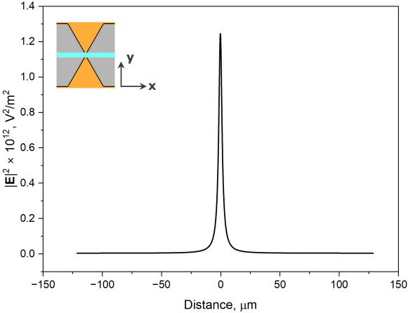
It is seen from Eq. (S2) that the nanoparticle radius can be found from the difference of the electric field amplitude squared estimated at the corresponding surface coordinates x and y. We calculate the Au nanoparticle radii by taking the numerically simulated electric field values (see Figure S5) and assuming perfectly polarizable Au spheres , T = 300 K, and .
Optimization of the experimental conditions
It is known that applying an electric field to a microfluidic system generates a series of effects on the fluid itself, including electrothermal (ET) flow, electroosmosis and natural convection, which can induce particle movement via the Stokes drag force [S5]. While this drag and other forces such as gravity and buoyancy could influence the measurement and have been discussed in the literature in great detail [S5, S6–S10], we focus here only on the two electrokinetic effects clearly observed in our experiments – DEP and ET effects – and how to keep them under control.
The ET effect also exists in highly inhomogeneous electric fields and induces two forces acting on a liquid: Coulomb and dielectric forces [S6, S11–S13]. The dominance of one or the other depends on the frequency range and determines the fluid flow direction, since both forces act in opposite directions. Hence, the fluid movement is minimal at the frequency where the transition between these two forces occurs. Besides, the fluid flow velocity determines the magnitude of the drag force for particles. In very high conductivity media, its magnitude may vastly exceed the DEP force, causing particles to follow the direction of the fluid flow. Such a particle behavior would refute our hypothesis that convection can be disregarded in Eq. (4) of the main text and we must ensure that the ET effect is suppressed in our DEP experiments.
The simplest way to suppress fluid flow is to reduce the liquid conductivity and its nonuniform heating to the lowest possible value. In this work, all DEP experiments were performed in water with a low conductivity of 16 S/cm. Nevertheless, when we applied a sinusoidal signal with the amplitude of = 15 V and frequency of 500 kHz, we still observed rapid particle movement that is uncommon for DEP (see Video S1): particles circulated above the electrodes rather than being stably trapped in the gap between them. Detecting the depletion region in these conditions was impossible (Figure S6). Assuming that the ET effect is responsible for this particle movement, we gradually increased the electric field frequency up to 5 MHz, reaching the transition frequency between Coulomb and dielectric forces, where the fluid movement vanishes and DEP dominates (see Video S2). In this series of experiments, the optimum frequency of 3 MHz was determined, which is in agreement with the ET theory [S5, S6].
The second important factor that must be considered is the DEP electrode geometry. Indeed, along with generating a strong electric field to build well-discriminated depletion regions, the electrodes must also ensure sufficient space between adjacent DEP traps to prevent overlapping depletion regions. The effect of this intersection can be readily observed in the simulations of our DEP device when the distance between the gaps of two neighboring sawtooth electrode pairs is reduced from 250.4 m to 83.5 m (see Figure S7). In this case, the concentration profiles near each electrode pairs merge, which blurs their boundaries. Therefore, one must carefully optimize the electrodes geometry and experimental conditions such that there is a spacing of at least two times the depletion region.
References
[S1] Madou, M. J. Manufacturing Techniques for Microfabrication and Nanotechnology; CRC press, 2011; Vol.2.
[S2] Abasahl, B.; Santschi, C.; Raziman, T. V.; Martin, O. J. F. Nanotechnology 2021, 32, No. 475202.
[S3] Zavatski, S.; Bandarenka, H.; Martin, O. J. F. Anal. Chem. 2023, 95, 2958–2966.
[S4] Loucaides, N. G.; Ramos, A.; Georghiou, G. E. Journal of Electrostatics 2011, 69 (2), 111–118.
[S5] Castellanos, A.; Ramos, A.; Gonzalez, A.; Green, N. G.; Morgan, H.; Journal of Physics D 2003, 36 (20), 2584.
[S6] Ramos, A.; Morgan, H.; Green, N. G.; Castellanos, A. Journal of Physics D: Applied Physics 1998, 31 (18), 2338–2353.
[S7] Green, N. G.; Morgan, H.; Milner, J. J. Journal of Biochemical and Biophysical Methods 1997, 35 (2), 89–102.
[S8] Green, N. G.; Ramos, A.; Morgan, H. Journal of Physics D: Applied Physics 2000, 33 (6), 632–641.
[S9] Green, N. G.; Morgan, H. Journal of Physical Chemistry B 1999, 103 (1), 41–50.
[S10] Green, N. G.; Ramos, A.; González, A.; Castellanos, A.; Morgan, H. Journal of Physics D: Applied Physics 2000, 33 (2).
[S11] Green, N. G.; Ramos, A.; González, A.; Castellanos, A.; Morgan, H. Journal of Electrostatics 2001, 53 (2), 71–87.
[S12] Salari, A.; Navi, M.; Lijnse, T.; Dalton, C. Micromachines 2019, 10 (11), 1–27.
[S13] Sun, H.; Ren, Y.; Hou, L.; Tao, Y.; Liu, W.; Jiang, T.; Jiang, H. Analytical Chemistry 2019, 91 (9), 5729–5738.
SUPPORTING FIGURES
