Inadequacy of equivalent circuits in nonlinear systems with inherent memory
Abstract
Basic multimode impedance analysis grounded in the availability of nonequilibrium charge carriers and their retarded path towards equilibrium is used to access the inadequacy of equivalent circuits in nonlinear systems with inherent memory. On the basic grounds of coexisting generation and trapping sites and their relaxation times, we show how seeming complexity of frequency-dependent impedance that matches a vast universe of experimental evidences can be reduced to simple combinations of basic microscopic ingredients. The emergence of counterintuitive features such as a negative capacitances or unexpected inductances becomes a metaphoric construction with poor physical meaning, pointing to the limitations and ambiguities of the symbolic nature of “equivalent” circuits. Our approach further provides a microscopic perspective that exposes the linkage of an apparent flux with an apparent inductance dismissing any magnetic essence.
Be it intentional or not, the nonlinear response of conductive systems or the nonlinear operation of electronic devices are widely present and appear in redox reactions at the surface of metamaterials Priyadarshani et al. (2021), leaking currents in solar cells Guerrero et al. (2016), memristive effects in the conduction of semiconductor oxides de Paiva et al. (2022), electrochemical processes within energy storage components Luo et al. (2022), memory functionalities of nanoscopic transistors Miller et al. (2021), among many other systems. In frequency domain, these nonlinear effects are characterized by combining cyclic voltammetry and impedance spectroscopy (IS) Wang et al. (2021) with the purpose to understand their driving mechanisms while quantifying the ruling parameters. When the transport response deviates from linearity, a set of challenges emerges Kowal et al. (2009) such as the impedance dependence on the pulse amplitude Fasmin and Srinivasan (2017) and higher mode generation Kiel et al. (2008); Pershin et al. (2021). Both are linked to the microscopic carrier dynamics, which is an often overlooked connection. Another challenge is the effort to translate the nonlinear response in terms of combinations of “equivalent” linear circuit elements and subsequently trying to ascribe physical meaning to them. Inconsistencies may appear in the interpretation of IS results Mei et al. (2018) forcing some behaviors to be put in perspective such as seemingly inductive effects Guerrero et al. (2016); Klotz (2019); Bou et al. (2020); Abdulrahim et al. (2021); Priyadarshani et al. (2021); Gonzales et al. (2022); Thapa and Gao (2022), the so called negative capacitance Jonscher (1986); Ershov et al. (1998); Mora-Seró et al. (2006); Ebadi et al. (2019); Joshi et al. (2020), and even some apparent capacitive responses perhaps unrelated to electric displacement Irvine et al. (1990); Liu et al. (2005); Das et al. (2008); Li et al. (2013); Nowroozi and Clemens (2018); Vadhva et al. (2021).
Here, we demonstrate how naturally emerging dynamics in nanoscopic nonlinear systems with inherent memory leads to the inadequacy of equivalent circuit representations and how seemingly unphysical responses emerge from the mapping of these dynamical systems onto steady state classical passive circuit elements. To meet these challenges, we take advantage of the multimodal characterization of nonlinear systems Fasmin and Srinivasan (2017) in combination with a microscopic perspective of systems driven out of equilibrium. We show how the interplay between competing intrinsic timescales and symmetry of generation functions of coexisting of independent transport channels impose the need to perform multimodal characterization beyond the fundamental system response. Although a multimode analysis could pose experimental challenges due to eventual noise interference for small signals, there is no alternative if the purpose is a full characterization of intrinsic properties that drastically affect the system response or the device operation.
The generation or trapping of nonequilibrium carriers affects the conductance of nanoscopic devices and can originate from various (independent) nonequilibrium generation/trapping mechanisms e.g., electrons trapped in deep or shallow defects de Paiva et al. (2022), the diffusion of ionic species, the contributions of different ionic species adsorbed on a surface Messerschmitt et al. (2015). Within the relaxation time approximation, the carrier concentration fluctuation, , towards equilibrium can be written as
| (1) |
with being the relaxation time. The generation and trapping rates are described by the function , being respectively positive or negative. It contains microscopic information on the nature of these processes such as thermal activation, quantum tunneling, etc., along with the dependence on external parameters, e.g. electric field and temperature. Note that Eq. 1 is not new but is often treated as a weak perturbation in steady state approximations. The approximation fails for nanoscopic devices driven within the time range of a relaxation time of any given charging or trapping mechanism. It is worth noting that, independently on the initial conditions, a stable solution can be reached for Eq. 1 after a transient forming process, by applying and waiting “enough” de Paiva et al. (2022), that could be challenging under very slow dynamics. Going explicitly beyond the steady state approximation and taking the polarity dependence of the generation function into account has severe consequences in the mapping of state dynamics, shedding light on the flaws of using equivalent circuits for this purpose.
The memory resistance emerging from the state dynamics in Eq. 1 can be emulated using the Drude like conductance Silva et al. (2022), where the nonequilibrium carriers, , contribute as
| (2) |
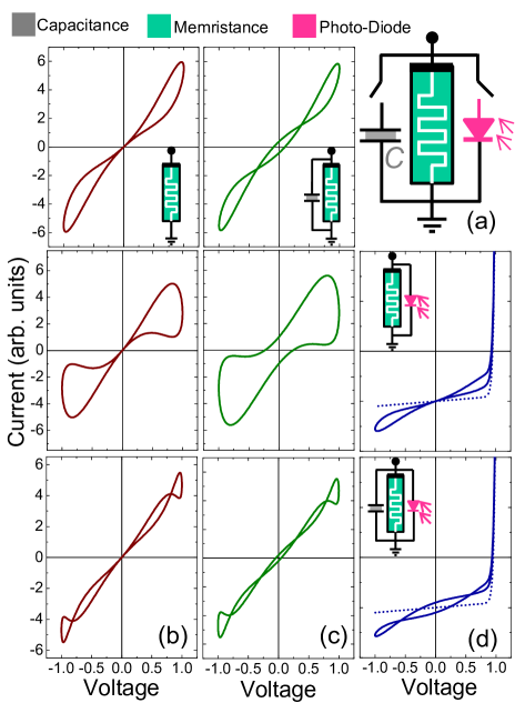
according to their mobility, , with and being the distance between contacts, while is the unperturbed conductance. In order to extend the picture, a capacitive coupling, be it intentional or parasitic, can be explicitly considered using a capacitance, , as illustrated in Figure 1 (a). In our model this capacitance will not be linked to any resistive switching mechanism Messerschmitt et al. (2015).
Driven by a time-periodic voltage, , the generation or trapping provokes a rich variety of effects in the current voltage plane Lopez-Richard et al. (2023) as illustrated in Figure 1 (b) where memory responses can be identified leaving out any capacitive coupling, . If a capacitive coupling is available it can be emulated by adding the term, , to Eq. 2. Its contribution can be traced down to openings in the current-voltage loops at , as shown in column Figure 1 (c). The coexistence of independent generation or trapping mechanisms enters the forthcoming discussion and its effects have been exemplified at the bottom of columns (b) and (c) in Figure 1. An analogous approach can be applied to the emulation of photo-diodes as presented in the Supplementary Material. Also, in the case of a photo-diode, the retarded dynamics with the contribution of a leaking channel has been illustrated in Figure 1 (d). The memory effect contrasts with the unperturbed photo-diode response and the hysteresis opens at , for .
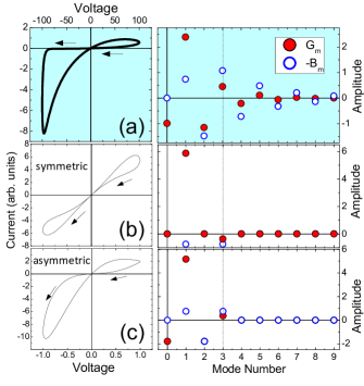
Examples of stable cycles have been displayed for a single charging mechanism in Figures 2. Panel (a) is consistent with a polarity dependent memristive response using, for the generation function of Eq. 1, the model reported in Ref. 28. The corresponding Fourier coefficients for this current-voltage response have been displayed in the right side of the panel. The fact that the response contains higher Fourier modes Kiel et al. (2008); Fasmin and Srinivasan (2017), than those present in the driving voltage input, is unavoidable in nonlinear dynamical systems as described in the Methods Section. The Fourier coefficients in Figure 2 depend on the applied voltage amplitude and a rich combination of signs can be identified that we shall further explore. Thus, in order to characterize nonlinearities, memory emergence effects, and avoid losing microscopic information, it is paramount to look beyond the first order mode.
For small relative signal amplitudes, as those used in IS, the generation/trapping rate can be decomposed up to second order on the applied voltage, . A system is called inversion symmetric if the transformation does not change its response. For such systems and the second order contribution becomes relevant. In the second order approximation, all the microscopic information resides within and . Their sign, relative strength, along with the voltage polarity (relevant for the term) define whether , for a trapping or, for the generation character of the sites of nonequilibrium carriers. Furthermore, Eqs. 1 and 2 can be analytically solved under this approximation resulting, for just a single mechanism, in
| (3) | ||||
Here, and are frequency independent parameters that contain not just intrinsic microscopic information and may change sign according to the trapping or detrapping nature of the given component, but also depend on the applied voltage amplitude. The multimode expansion for small amplitudes, in Eq. 3, stops at third order and has been exemplified in Figures 2 (b) and (c) by setting : one with inversion symmetry () and another one with polarity dependent response (), respectively. The first results in a Type II memristive response (symmetric and noncrossing at ) and the latter, in a Type I (asymmetric with a crossing at ).
Besides the trivial capacitive term, when in Eq. 3, the presence of dephasing proportional to , along all the modes can be interpreted as signatures of apparent reactive contributions. This points to the natural emergence of a dependence of the conductance on the apparent flux, , that has been a disputed missing connection for unambiguous definitions of memristors Chua (1971). Then, as reported in Ref. 32, no real inductive effects are needed to explain such a link that emerges in our case from the simple and ubiquitous nonequilibrium dynamics.
The first line of Eq. 3 consists of a order contribution to the current that arises from odd components to the generation function, available just in the absence of inversion symmetry, along with the capacitive term proportional to the geometric capacitance, , that contributes to the fundamental mode, . The second and third line also contribute to the fundamental mode resulting in an admittance for , as defined in the Methods Section, given by
| (4) | ||||
The corresponding admittance of and is, respectively
| (5) |
and
| (6) |
One may note the resistive contribution of the first line of Eq. 4 with an effective resistance and the trivial capacitive addition in the third if . In turn, given that , , , and are frequency independent parameters, there is a common pattern in the functional dependence on of the second line of Eq, 4 and also in Eqs. 5 and 6. We can thus draw an analogy between these cases and the admittance of a series element,
| (7) |
with . Yet, the equivalency is just apparent, since there is clearly no inductive effect assumed in order to obtain the results of Eq, 4, 5, nor 6. There is also clearly no point to ascribe this kind of admittance to an element, as represented in Figure 3 (a) as often done, given the lack of displacement currents when . The approach, intended to parameterize admittance components analogous to Eq. 7 with equivalent circuits, has resulted in puzzling frequency tuning of the equivalent capacitance Jonscher (1986); Ershov et al. (1998); Mora-Seró et al. (2006); Ebadi et al. (2019); Joshi et al. (2020); Irvine et al. (1990); Liu et al. (2005); Das et al. (2008); Li et al. (2013); Nowroozi and Clemens (2018); Vadhva et al. (2021). The flaw emerges when trying to emulate the natural -like frequency dependence of the admittance, as those presented in Eqs. 4-7, with the expected frequency dependence of an element, , that artificially forces an additional frequency dependence of both and and, sometimes, unexpected signs for them.
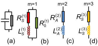
We recommend replacing the “equivalent” designation of auxiliary circuits with the label apparent in the case of nonlinear responses. The use of apparent circuits, as compact, symbolic, and intuitive representations of the system response can be useful and we have provided them for (setting ) in panels (b), (c), and (d) of Figure 3, according to the functional dependence on frequency of the admittance obtained by the microscopic approach. Here, , , , , , and . However, ascribing a physical meaning to these circuit components beyond the parametric correlation just written can be fruitless. Note that it is expected for them to naturally change sign according to the sort of the generation function components ( or ). Although being independent of frequency and holding all the microscopic information, these effective parameters depend on the input amplitude and thus cannot be interpreted as intrinsic properties decoupled from the external drive.
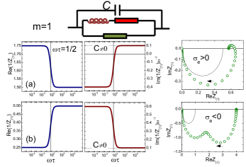
We will keep using the symbolic value of these apparent circuits but we will not refer to these circuits elements as real and proceed to analyze the main features expected of the impedance per mode focusing on Eqs. 4, 5, and 6. The frequency response will be depicted using Bode plots for a resistive like, , and a reactive like component, , complemented with the corresponding Nyquist’s maps. We should note that it is common to find the expression, , identified as an “efective capacitance”, , due to the trivial relation expected for a capacitive impedance, where . We will not use this identification in order to avoid a potential confusion with a real capacitance, , that may be present in the circuit. For and a single mechanism, according to Eq. 4,
| (8) |
and
| (9) |
Both components depend on frequency and this emerges from the charging or trapping retardation of nonequilibrium carriers contributing to the conductance. However this kind of functional dependence has been the source of erroneous interpretations, mainly when the reactive component is incorrectly ascribed to a dielectric modulation of a capacitance within the system, which is not the case. The resulting impedance analysis for is depicted in Figures 4 (a) and (b) for generation and trapping sites, respectively. The step-like behavior in the logarithmic frequency scale appears at (half step height) that matches the condition for maximum hysteresis area reported in Ref. 28 for Type II memristive responses. The size of the step, in turn, depends on the carrier mobility, the even component of the generation/trapping efficiency, , the relaxation time, and voltage amplitude, contained within . Given the dependence of on , the steps in the left panels scale as , while in the middle as . More importantly, the reactive components in Eq. 9 can be positive or negative according to the sign of and even change sign if leading to the deceptive labels of negative capacitance or inductive contributions with nonmagnetic origin. This can also be identified in the corresponding Nyquist’s maps, where arrows point to the frequency growth direction. These are very common figures found in metamaterials with memory traces. They have been labeled in the literature as traces of negative or positive capacitance Jonscher (1986); Ershov et al. (1998); Mora-Seró et al. (2006); Li et al. (2013); Ebadi et al. (2019) because of the resemblance to the semicircular maps, or instead as inductive-like responses Joshi et al. (2020); Priyadarshani et al. (2021); Gonzales et al. (2022), for analogous reasons.
If the capacitive coupling, whether intentional or not, is different from zero, the effect of the reactive part always vanishes in the limit of very high frequencies down or up to the capacitive leftover, , similar to a variety of experimental evidences as those reported for instance in Refs. 18; 19; 21. The corresponding Nyquist’s plots exhibit also the interference of this capacitive effect, that has been singled out by plotting the impedance in the absence of nonequilibrium carriers, , as a continuous curve.
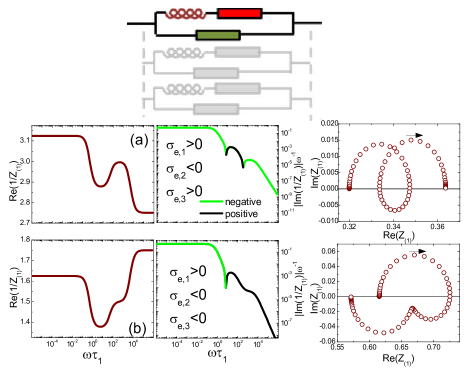
A single generation or trapping mechanism already provides useful insights. However, often more processes are simultaneously happening such as concomitant ionic and electronic transport. The contribution of additional independent channels to the admittance is additive and the analysis can be readily extended to that case as described in the Methods Section. This has been exemplified in Figure 5 for considering three concomitant channels with contrasting relaxation time scales, combining generation and trapping mechanisms (for simplicity we left in this case). We have introduced logarithmic vertical axes in the middle panels of Figure 5 since unlike the sequential steps in the left panels that scale as , the steps in the middle panels scale as as discussed previously. Note, that we report the absolute value, , in panels (a) and (b), where the function sign has been identified with contrasting lines. The non-monotonic trends of both resistive and reactive components and the sign of the latter emerge from the same nonequilibrium dynamics following the character of according to the sequence of the relaxation times, . Once again, these behaviors have been interpreted incorrectly as traces of negative capacitance or inductive effects. These patterns can be recognized, for instance, in the experiments reported in Refs 17; 33; 34; 2; 15. Also the shape of the corresponding Nyquist’s maps changes drastically according to the time-scale sequencing of the contributing mechanisms. The combination of channels with identical generation or trapping nature has been illustrated in the Supplementary Material.
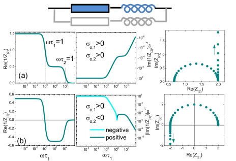
Note that the contributions from Eq. 3 proportional to the odd component of the generation rate, , (embedded in ), and all the information related to eventual inversion asymmetries and polarity would have been overlooked by just analyzing the fundamental mode, . Thus, in order to obtain a full picture of all contributing elements to the transport response, the impedance analysis must look beyond . The effects of adding independent channels has been illustrated in Figures 6 (a) and (b) for . Again, a step-like behavior appears as the frequency is spanned across the marks, , for for charging mechanisms with the same character, corresponding to the example in panel (a). Yet, changes in sign in panel (b) occur for alternating sign during the sequential tuning of charging mechanisms with frequency. The resistive and reactive part of the impedance can be either positive or negative according to the nature of . For all the above cases the admittance for coexisting channels still collapses as . The spectra for a single channel and can be found in the Supplementary Material. In this approximation, according to Eqs. 4 and 6, the information contained in the impedance of the mode could appear redundant to the one for . However, one must point that while the fundamental mode, , contains the interference of both and , the third order mode is fully independent on them, holding just the microscopic information enclosed within , and this can be useful if discernible. The corresponding impedance maps for have been condensed in the Supplementary Material.
In summary, avoiding a multimode perspective when studying nonlinear transport responses may hinder a complete understanding of the causes and nature of the emergence of memory traces. It is thus recommended to try to match multimode impedance analyses with theoretical models starting with the simplest possible microscopic approach and gradually add complexity when necessary. As demonstrated here, conventional approaches can already provide relevant clues for seemingly complex and unrelated behaviors. This also highlights the importance of building apparent circuit representations starting from a microscopic perspective and not the other way around, recognizing the limitations in the interpretation associated to the apparent circuit components. Thus, the emergence of counterintuitive features such as a negative capacitances or unexpected inductances (in the absence of any magnetic ingredients or eventual displacement currents) becomes just a representation metaphor and not a consequence of anomalous physical behaviors. Clearly, real capacitive effects, that lead to displacement currents, or inductive features, magnetic in nature, cannot be ruled out when characterizing transport properties. However, as we tried to prove here, the mere availability of nonequilibrium charges and their retarded path towards equilibrium are already sufficient ingredients to provide a very rich impedance response that matches a vast range of experimental evidences.
Methods The transport characteristics that emerges in nonlinear dynamic systems under alternating input, , at steady state, can only be reconstructed by a specific combination of higher order harmonics, as
| (10) |
This multimode response allows defining an admittance, or inversed impedance, per mode, independent on time,
| (11) |
where can be interpreted as being the -mode conductance and , the -mode susceptance. Such definitions emerge in compliance with the traditional way the spectral information is tackled in the impedance analysis for the fundamental (and only) mode, , in linear responses.
When independent generation and/or trapping mechanisms contribute simultaneously, Eq. 1 transforms to
| (12) |
with for small relative signals. Here, the index labels each independent transport channel, transforming the total current in Eq. 2 as
| (13) |
The corresponding admittance per mode are thus given in this case by
| (14) | ||||
| (15) |
and
| (16) |
Here and .
Acknowledgments This study was financed in part by the Conselho Nacional de Desenvolvimento Científico e Tecnológico - Brazil (CNPq) Projs. 301033/2019-6 and 131951/2021-1, and the Fulbright Program of the United States Department of State’s Bureau of Educational and Cultural Affairs.
References
- Priyadarshani et al. (2021) D. Priyadarshani, D. Choudhury, M. E. Joy, A. Kottantharayil, and M. Neergat, The Journal of Physical Chemistry C 125, 27736 (2021).
- Guerrero et al. (2016) A. Guerrero, G. Garcia-Belmonte, I. Mora-Sero, J. Bisquert, Y. S. Kang, T. J. Jacobsson, J.-P. Correa-Baena, and A. Hagfeldt, The Journal of Physical Chemistry C 120, 8023 (2016).
- de Paiva et al. (2022) A. B. de Paiva, R. S. Wengenroth Silva, M. P. F. de Godoy, L. M. Bolaños Vargas, M. L. Peres, D. A. W. Soares, and V. Lopez-Richard, The Journal of Chemical Physics 157, 014704 (2022).
- Luo et al. (2022) Y. Luo, Y. Zhao, J. Ma, Y. Huang, S. Han, M. Zhou, and H. Lin, The Journal of Physical Chemistry C 126, 18229 (2022).
- Miller et al. (2021) K. Miller, F. Hartmann, B. Leikert, S. Kuhn, J. Gabel, M. Sing, R. Claessen, and S. Höfling, Applied Physics Letters 118, 153502 (2021).
- Wang et al. (2021) S. Wang, J. Zhang, O. Gharbi, V. Vivier, M. Gao, and M. E. Orazem, Nature Reviews Methods Primers 1, 41 (2021).
- Kowal et al. (2009) J. Kowal, D. Hente, and D. U. Sauer, IEEE Transactions on Instrumentation and Measurement 58, 2343 (2009).
- Fasmin and Srinivasan (2017) F. Fasmin and R. Srinivasan, Journal of The Electrochemical Society 164, H443 (2017).
- Kiel et al. (2008) M. Kiel, O. Bohlen, and D. Sauer, Electrochimica Acta 53, 7367 (2008), 7th International Symposium on Electrochemical Impedance Spectroscopy.
- Pershin et al. (2021) Y. V. Pershin, C.-C. Chien, and M. Di Ventra, Journal of Physics D: Applied Physics 54, 245302 (2021).
- Mei et al. (2018) B.-A. Mei, O. Munteshari, J. Lau, B. Dunn, and L. Pilon, The Journal of Physical Chemistry C 122, 194 (2018).
- Klotz (2019) D. Klotz, Electrochemistry Communications 98, 58 (2019).
- Bou et al. (2020) A. Bou, A. Pockett, D. Raptis, T. Watson, M. J. Carnie, and J. Bisquert, The Journal of Physical Chemistry Letters 11, 8654 (2020).
- Abdulrahim et al. (2021) S. M. Abdulrahim, Z. Ahmad, M. Q. Mehmood, S. Paek, J. Bhadra, N. J. Al-Thani, M. K. Nazeeruddin, A. Belaidi, and M. Amani, Journal of Electroanalytical Chemistry 902, 115800 (2021).
- Gonzales et al. (2022) C. Gonzales, A. Guerrero, and J. Bisquert, The Journal of Physical Chemistry C 126, 13560 (2022).
- Thapa and Gao (2022) A. Thapa and H. Gao, Journal of The Electrochemical Society 169, 110535 (2022).
- Jonscher (1986) A. K. Jonscher, J. Chem. Soc., Faraday Trans. 2 82, 75 (1986).
- Ershov et al. (1998) M. Ershov, H. Liu, L. Li, M. Buchanan, Z. Wasilewski, and A. Jonscher, IEEE Transactions on Electron Devices 45, 2196 (1998).
- Mora-Seró et al. (2006) I. Mora-Seró, J. Bisquert, F. Fabregat-Santiago, G. Garcia-Belmonte, G. Zoppi, K. Durose, Y. Proskuryakov, I. Oja, A. Belaidi, T. Dittrich, R. Tena-Zaera, A. Katty, C. Lévy-Clément, V. Barrioz, and S. J. C. Irvine, Nano Letters 6, 640 (2006).
- Ebadi et al. (2019) F. Ebadi, N. Taghavinia, R. Mohammadpour, A. Hagfeldt, and W. Tress, Nature Communications 10, 1574 (2019).
- Joshi et al. (2020) S. M. Joshi, N. Xia, Y. Berta, Y. Ding, R. A. Gerhardt, E. Woods, and M. Tian, MRS Communications 10, 278 (2020).
- Irvine et al. (1990) J. T. S. Irvine, D. C. Sinclair, and A. R. West, Advanced Materials 2, 132 (1990).
- Liu et al. (2005) J. Liu, C.-g. Duan, W. N. Mei, R. W. Smith, and J. R. Hardy, Journal of Applied Physics 98, 093703 (2005).
- Das et al. (2008) N. Das, S. Tsui, Y. Y. Xue, Y. Q. Wang, and C. W. Chu, Phys. Rev. B 78, 235418 (2008).
- Li et al. (2013) Y. Li, Y. P. Zhong, J. J. Zhang, X. H. Xu, Q. Wang, L. Xu, H. J. Sun, and X. S. Miao, Applied Physics Letters 103, 043501 (2013).
- Nowroozi and Clemens (2018) M. A. Nowroozi and O. Clemens, ACS Applied Energy Materials 1, 6626 (2018).
- Vadhva et al. (2021) P. Vadhva, J. Hu, M. J. Johnson, R. Stocker, M. Braglia, D. J. L. Brett, and A. J. E. Rettie, ChemElectroChem 8, 1930 (2021).
- Lopez-Richard et al. (2023) V. Lopez-Richard, R. S. W. Silva, O. Lipan, and F. Hartmann, Journal of Applied Physics 133, accepted (2023).
- Messerschmitt et al. (2015) F. Messerschmitt, M. Kubicek, and J. L. M. Rupp, Advanced Functional Materials 25, 5117 (2015).
- Silva et al. (2022) R. S. W. Silva, F. Hartmann, and V. Lopez-Richard, IEEE Transactions on Electron Devices 69, 5351 (2022).
- Chua (1971) L. Chua, IEEE Transactions on circuit theory 18, 507 (1971).
- Strukov et al. (2008) D. B. Strukov, G. S. Snider, D. R. Stewart, and R. S. Williams, Nature 453, 80 (2008).
- Almora et al. (2015) O. Almora, I. Zarazua, E. Mas-Marza, I. Mora-Sero, J. Bisquert, and G. Garcia-Belmonte, The Journal of Physical Chemistry Letters 6, 1645 (2015).
- Pivac et al. (2017) I. Pivac, B. Šimić, and F. Barbir, Journal of Power Sources 365, 240 (2017).
SUPPLEMENTARY MATERIAL
The model can be extended for the simulation of the effects of leaking or shunting transport channels in photo-diodes (or solar cells). In this case the current can be tuned by the non nonequilibrium dynamics as
| (17) |
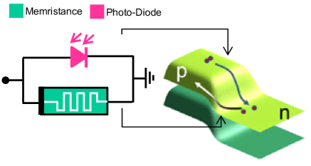
where and are the illumination and saturation currents, respectively. An additional capacitive coupling between contacts can be emulated by adding the term, to Eq. 17. The transport channels are represented in Figure 7 including a leaking path for nonequilibrium carriers that corresponds to the third term on the right hand side of Eq. 17. It exhibits a memristive nature.
In the case of the current described by Eq. (3) of the manuscript, the admittance per mode, up to third order approximation, is given by the expressions
| (18) | ||||
| (19) |
and
| (20) |
The index labels each generation or trapping mechanism available.
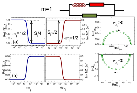
The frequency response is characterized using Bode plots for and , along with the corresponding Nyquist’s maps. For and a single mechanism, according to Eq. 18, and . The results, for , and just are shown in Figures 8 (a) and (b) for detrapping and trapping sites, respectively. The step-like behavior in the logarithmic frequency scale appears at (half step height) that exactly matches the condition for maximum hysteresis area reported in Ref. 28 for Type II (noncrossing and symmetric) memristive responses. The size of the step, indicated in Figure 8 (a) depends on the carrier mobility, the even component of the generation/trapping efficiency, , the relaxation time, and voltage amplitude, contained within .
The conductive state undergoes a transition from a low to a high resistive condition as the frequency grows for detrapping sites, in Figure 8 (a) and vice versa in the case of trapping sites, depicted in Figure 8. This can also be identified in the corresponding Nyquist’s maps, where arrows point to the frequency growth direction. Under these conditions the maps become semicircles with radius , where , spanning either positive reactance values, for , or negative ones, if . These are common figures found in metamaterials and have been labeled in the literature as traces of negative or positive capacitance because of the resemblance to the semicircular maps, or instead as inductive-like responses for analogous reasons.
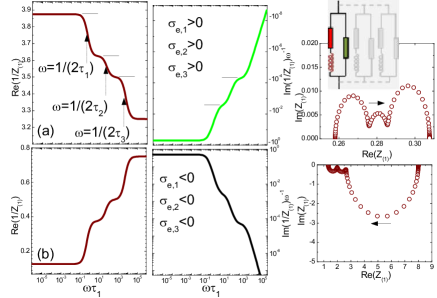
The case of coexisting charging mechanisms has been exemplified in Figure 9 for considering three concomitant channels with contrasting relaxation time scales, (and ). Panels (a) and (b) correspond to channels with identical detrapping or trapping nature, respectively. The reactive contribution of these channels is sequentially filtered out as the frequency grows beyond the marks for . Note that we have introduced logarithmic vertical axes in the middle panels of Figure 9 since unlike the sequential steps in the left panels that scale as , the steps in the middle panels scale as . For instance, as marked in Figure 9 (a), the sequence of plateaus for correspond to (for ), , , and finally when . While jumps from (for ) to and then to before collapsing to zero as . As exemplified in panel (b), dynamics with very large relaxation times may drastically distort the impedance map. These distortions appear at extremely slow frequencies and may be difficult to experimentally measure.
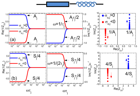
The impedance spectra for and have been represented in Figures 10 (a) and (b), following Eqs. 19 and 20 for one channel. The real and imaginary parts of the admittance tend to zero (collapse) for both modes as , and the transition (in the logarithmic frequency scale) occurs at for . This condition coincides with the optimal memristive Type I (self-crossing) response as discussed in Ref. 30. For , both the resistive and reactive part of the impedance can be either positive or negative according to the nature of . The relative height and positions of the steps are indicated within these panels.