Present address: ]Institute of Physics, University of Amsterdam, 1012WX Amsterdam, Netherlands
Bulk and surface electronic structure of Bi4Te3 from calculations and photoemission experiments
Abstract
We present a combined theoretical and experimental study of the electronic structure of stoichiometric Bi4Te3, a natural superlattice of alternating Bi2Te3 quintuple layers and Bi bilayers. In contrast to the related semiconducting compounds Bi2Te3 and Bi1Te1, density functional theory predicts Bi4Te3 to be a semimetal. In this work, we compute the quasiparticle electronic structure of Bi4Te3 in the framework of the approximation within many-body perturbation theory. The quasiparticle corrections are found to modify the dispersion of the valence and conduction bands in the vicinity of the Fermi energy, leading to the opening of a small indirect band gap. Based on the analysis of the eigenstates, Bi4Te3 is classified as a dual topological insulator with bulk topological invariants (1;111) and magnetic mirror Chern number . The bulk results are used to build a Wannier-functions based tight-binding Hamiltonian that is further applied to study the electronic properties of the (111) surface. The comparison with our angle-resolved photoemission measurements shows excellent agreement between the computed and measured surface states and indicates the dual topological nature of Bi4Te3.
I Introduction
The field of topological matter, both as a fundamental concept and as a search for materials for practical applications, is a very rapidly developing field [1, 2, 3]. Being based on the physics of spin-orbit coupling (SOC), topological insulators (TIs) show electronic properties fundamentally distinct from conventional insulators. Their surfaces are characterized by the existence of metallic surface states which are protected by time-reversal and spatial symmetries [4, 5, 6, 7]. Moreover, electrons in such states are spin polarized, and their spin angular moment orientation and propagation momentum are locked to each other. This property opens promising possibilities for the generation and control of dissipationless spin currents that might be exploited in practical applications in spintronics, quantum computation, and thermoelectronics.
Bi-Te alloys present a wide group of materials with intriguing and technologically important properties. These compounds have been known and intensively studied for a long time due to their thermoelectric properties. In addition, recently, a growing interest in these alloys has arisen after the discovery of non-trivial topological insulating properties that make them very promising candidates for future generation of electronic devices for spintronics and quantum computation [1].
Bi2Te3 is the first theoretically predicted and experimentally confirmed [8, 9, 1] prototype TI with surface states forming a single non-degenerate Dirac cone. It has been shown to be a strong TI (STI) with invariant (1;000) whose surface states are protected by time-reversal symmetry on all surfaces. It has been further shown that Bi2Te3 belongs to the family of topological crystalline insulators (TCI) with , where the presence of mirror symmetry leads to protection of the metallic surface states lying in the planes perpendicular to the mirror planes. Thus, Bi2Te3 was characterized as the first material predicted to be both a STI and a TCI. Since it exhibits this double topological nature, it was termed a dual TI [10]. With such a combination, one can potentially exploit the fact that controlled symmetry breaking would destroy certain surface states while keeping others intact.
In the quest for materials with targeted topological properties, an interesting direction of investigation is to combine layers of known topological compounds to form heterostructures [11]. For instance, an interface built by a bilayer (BL) of Bi(111) on a Bi2Te3 substrate has been studied as a prototype system that indeed combines properties of the two-dimensional (2D) and three-dimensional (3D) TIs such that topologically protected 1D edge and 2D surface states coexist at the surface [12].
In this context, it becomes interesting to study compounds that would combine the Bi bilayers (Bi2) and Bi2Te3 quintuple layers to create new stoichiometric bulk Bi-Te alloys. Bi1Te1, one such combination, was recently synthesized, characterized, and shown to be a dual 3D TI in which a weak TI phase and TCI phase appear simultaneously [13].
Bi4Te3 is another well-known natural superlattice of Bi2 and Bi2Te3 (see Fig. 1) whose topological properties are not yet thoroughly understood. In contrast to Bi2Te3 and Bi1Te1, this compound is considered to be a topological semimetal according to the Topological Materials Database [14]. Bi4Te3 has been seen to undergo a number of pressure-induced structural transformations to metallic phases that lead to distinct superconducting states [15]. Saito et al. [16] describe the Bi4Te3 bulk crystal taking SOC into account as a zero bandgap semimetal with a Dirac cone at the point. In all mentioned works, the theoretical analysis of the band structure was performed using density functional theory (DFT). By contrast, we go beyond DFT in this study and provide an analysis of the bulk and surface electronic structure of Bi4Te3 by employing the state-of-the-art quasiparticle approach based on many-body perturbation theory (MBPT). This technique was applied earlier to study the electronic properties of other topological materials, and the importance of quasiparticle effects has been established for these materials [17, 18, 19, 20, 21, 22, 23, 24, 25, 26]. The results for the constituents of Bi4Te3 (i.e., Bi2Te3 [24] and Bi [27]) also proved that the method significantly improves the results provided by DFT. In particular, in Ref. [27], we showed with the example of Bi, the difficulties in accurately describing the electronic structure of semimetals or very narrow bandgap semiconductors, and we highlighted the importance of using methods beyond DFT to study these kinds of materials accurately. Since Bi4Te3 contains layers of Bi, it is not surprising that one needs to resort to the method to predict the fine details of its electronic structure. In our approach, we perform calculations for the bulk, and in order to compute the surface electronic band structure, we further parameterize a tight-binding (TB) Hamiltonian with the help of Wannier functions [28]. The TB Hamiltonian is obtained by following the method described in Ref. [26], and thus it is calculated fully ab initio without the need for adjustable parameters. The calculation of bulk and surface states as well as surface resonances with this method allows us to provide a direct comparison between the computed spectra and results from the angle-resolved photoemission (ARPES) studies.
The structure of this work is as follows. We start with the description of the crystal structure of Bi4Te3 in Section II. Then we provide details of the theoretical (Sec. III) and experimental (Sec. IV) setups. In Section V.1, we characterize the bulk electronic structure and compare it with previous works. Then, in Section V.2, we present the surface band structure and analyze the dual topological nature of Bi4Te3, including its topological index. In Section VI, we perform a comparative analysis of the theoretical and experimental results. Finally, we conclude in Section VII.
II Crystal structure
The lattice structure of bulk Bi4Te3 is built as a stack of quintuple layers (QLs) of Bi2Te3 intercalated with Bi bilayers with a periodic crystal structure that can be expressed as [(Bi2)(Bi3Te3)]3. Both conventional and primitive unit cells are shown in Fig. 1. The primitive cell reflects the rhombohedral crystal symmetry (space group R-3m) and consists of 7 atoms (with 2 Te and 2 Bi non-equivalent atoms).
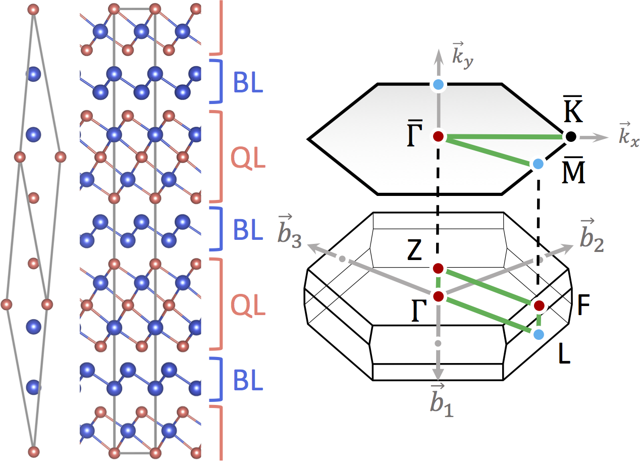
We employ the experimental lattice parameters of [29]. The primitive cell is determined by Å and , or using the conversion to the conventional (hexagonal) cell Å and Å. An optimization of the crystal structure (for details, see the Supplemental Material [30]) has revealed the lattice constants to be very close to the experimental ones: Å and . The optimized structure has a slightly (0.1 Å) smaller interlayer distance, which, keeping in mind the van der Waals type of bonding, has only a little influence on the electronic band structure (see Fig. 1 of the Supplemental Material [30]). Hence, in the following, the results are obtained with the experimental lattice parameters given above.
III Computational details
The electronic quasiparticle band structure is computed using the approximation of the MBPT. The calculations are performed employing the code spex [31], which implements the technique in the full-potential linearized augmented plane-wave (FLAPW) framework. The starting point for the calculations is provided through an interface to the FLAPW DFT code fleur [32]. The generalized gradient approximation (GGA) in the PBE parametrization [33] is chosen for the exchange-correlation potential. The core electrons are treated fully relativistically by solving the Dirac equation with the spherically averaged effective potential around each nucleus. For the valence electrons, space is partitioned into muffin-tin (MT) spheres and an interstitial region; in the former we use an angular momentum cutoff of and in the latter a plane-wave cutoff of 3.6 Bohr-1. The MT radii are set to 2.8 Bohr for all atoms. An 888 -point grid was used to sample the Brillouin zone.
The quasiparticle corrections are computed with the inclusion of SOC, which is known to have an important impact on the electronic properties of topological materials such as Bi2Te3 [22]. SOC is already included in the groundstate Kohn-Sham (KS) calculations, the KS eigenfunctions are thus single-particle spinor wavefunctions. We employ the second-variation technique [34], in which the SOC Hamiltonian is setup and diagonalized in the basis of KS states that have been precomputed without SOC. Specifically for this basis, we use the 400 KS states of lowest energy, which, in combination with other computational parameters, results in KS eigenenergies to be converged within 2 meV.
spex makes use of the auxiliary mixed product basis for representing matrix elements of the non-local operators. Based on our earlier experience [20] as well as performed convergence tests, we use the following parameters for the calculation. The mixed product basis is constructed by setting the maximal angular momentum for the muffin-tin spheres to and Bohr-1 for the interstitial part. For an accurate representation of the unoccupied states in the FLAPW method, additional basis function (so-called local orbitals) are included, two functions in each angular momentum channel with . A total number of about 1000 states (giving rise to about 880 empty states) corresponding to a maximal cutoff energy of eV are included for computing the screened Coulomb potential and the correlation self-energy. The Brillouin zone (BZ) integration is performed on an Monkhorst-Pack -point mesh. The contour deformation technique is used for the frequency convolution integration with 29 non-equidistant frequency points up to an (imaginary) energy of 272 eV along the imaginary axis. The self-energy is evaluated on a uniform grid with an increment of 0.54 eV along the real axis. Between the grid points, we employ spline interpolation. In this way, the self-energy is given as a continuous function along the real frequency axis, which allows us to solve the quasiparticle equation, which is nonlinear in frequency, without resorting to a linearization of the self-energy. The computational setup has been checked to provide the quasiparticle energies converged to within 15 meV. It should be mentioned that a 666 -point grid would be sufficient to reach reasonable energy convergence. However, such a grid turned out to be too coarse for an accurate Wannier interpolated band structure.
The Wannier-function based TB Hamiltonian is used further as an input to compute the surface projected electronic band structure employing the WannierTools [35] program package. In this work, we are interested in a narrow region of bands lying close to the Fermi level. These bands have a predominant character, which motivates us to set -type “initial-guess” Wannier functions for each inequivalent atom and perform the maximal localization procedure via an interface with the Wannier90 library [36].
IV Experimental details
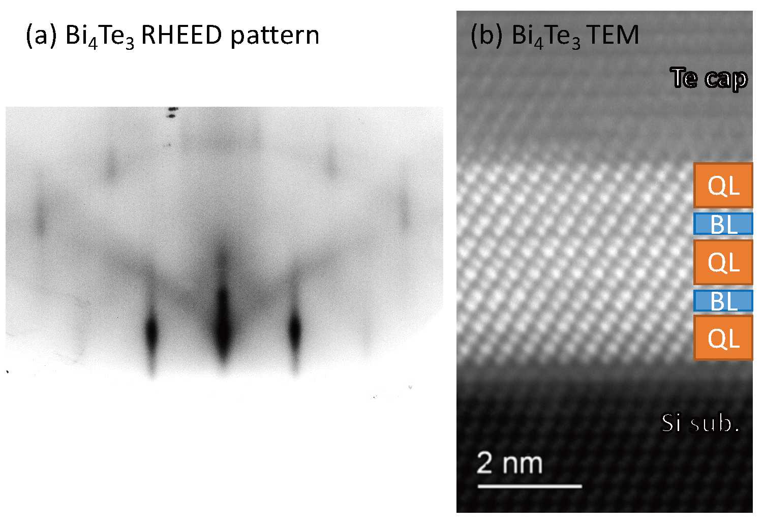
The samples were fabricated by the following procedure. First a clean Si(111)- surface was prepared on an -type substrate by a cycle of resistive heat treatments. Then, Bi was deposited on the structure at 250∘C under Te-rich conditions. Such a procedure is reported to result in a high-quality Bi2Te3(111) film formation [37]. Then, the grown films were annealed at 310∘C for 2 hours in ultra-high vacuum. During this process, Te was desorbed from the sample, and thus the sample became a Bi4Te3(111) film with the QL termination as confirmed by the transmission electron microscopy (TEM) observations. Figure 2 shows the reflection high-energy electron diffraction (RHEED) pattern (a) and the TEM image of a typical sample. The in-plane lattice constant was determined as 4.45 0.05 Å and the films were determined as two-unit-cells thick with an additional QL at the interface between the film and the substrate (or the wetting layer). Details of the sample preparation and structure characterization will be published elsewhere [38]. The ARPES measurements were performed in situ after the sample preparation with a commercial hemispherical photoelectron spectrometer equipped with angle and energy multidetections (MBS A1) at UVSOR BL-7U of UVSOR-III with eV photons [39]. The sample was cooled down to 16 K for the measurements.
V Results
V.1 Bulk band structure
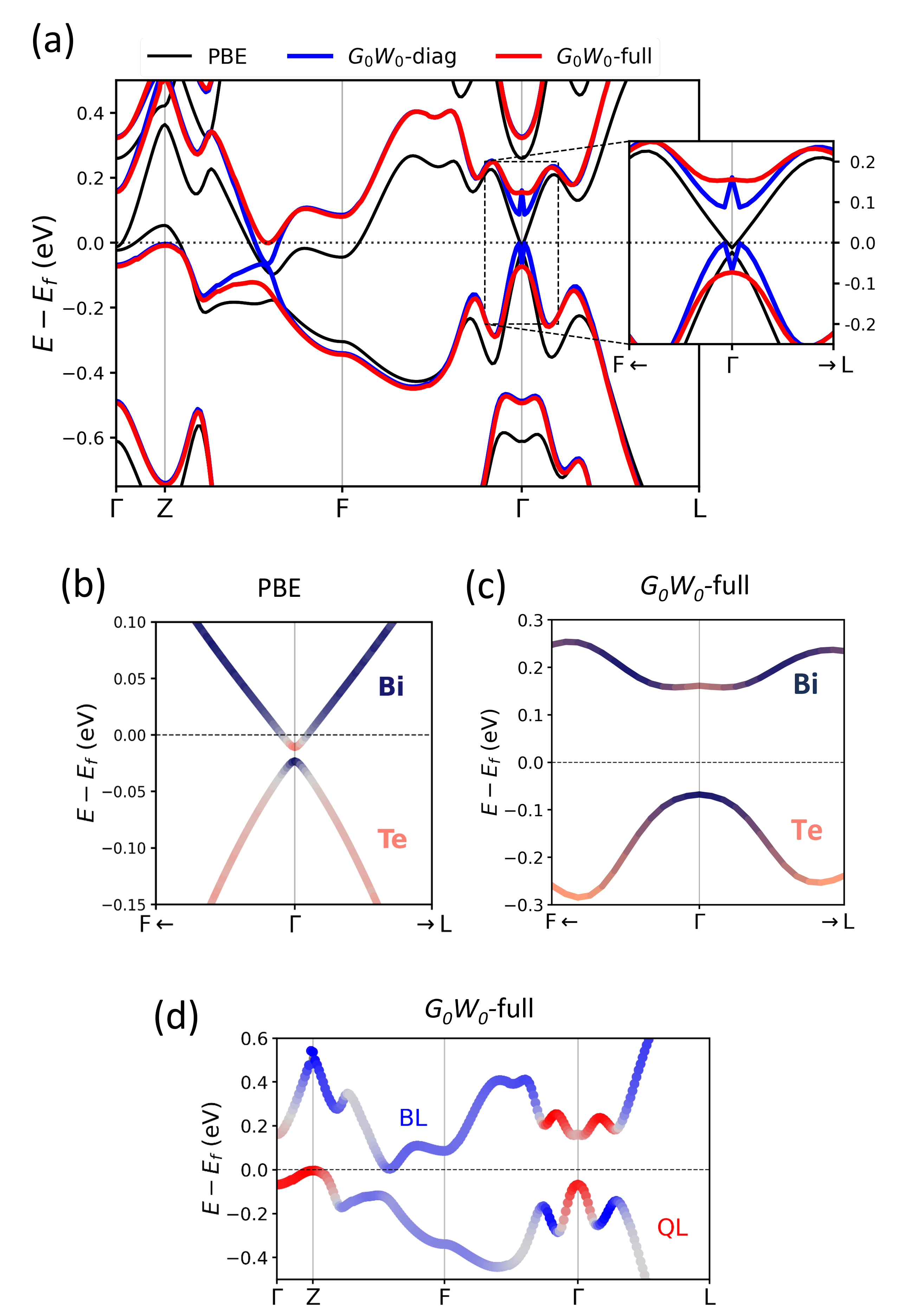
The electronic band structure of Bi4Te3 is presented in Fig. 3. The PBE band structure indicates that Bi4Te3 is a semimetal with a wide electron pocket along the Z–F -point path and a small hole pocket around the Z point. The valence (VB) and conduction (CB) bands are closely approaching each other at , where a band inversion takes place [see Fig. 3(b)]. In contrast to our results, the band structure presented in the Topological Materials Database [14] seems to exhibit a crossing of the VB and CB along the –Z in the vicinity of the Fermi level. On the other hand, our DFT band structure is in good agreement with the one of Ref. [16]. Our calculation yields an energy gap of 10 meV between the VB and CB at the point, and the CB minimum at this point is located slightly below the Fermi energy. The value of the gap turns out to be quite sensitive to the computational parameters. As it is shown in the Supplemental Material [30], the magnitude of the gap depends on the choice of the local orbital basis functions employed in the FLAPW method.
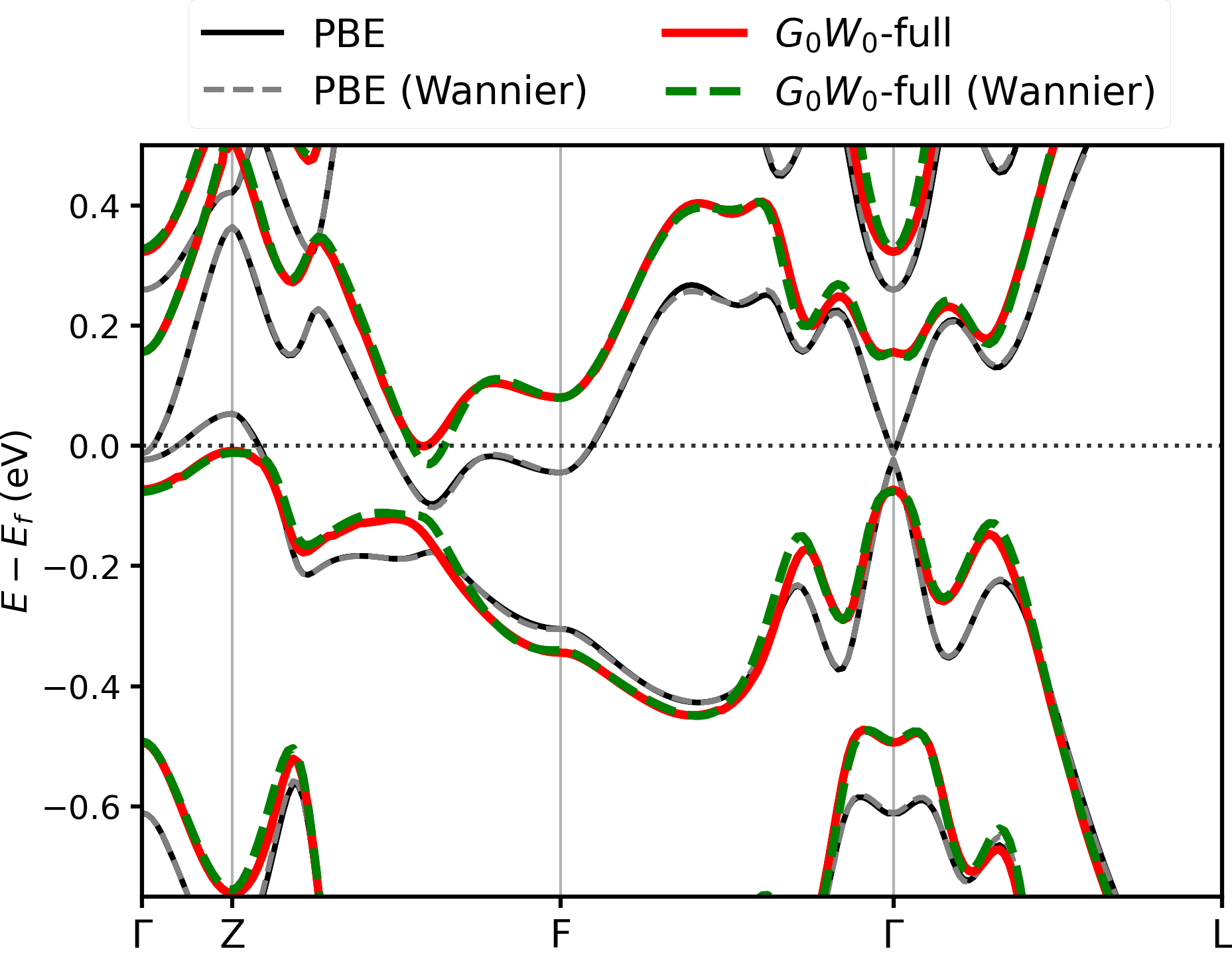
Adding the quasiparticle corrections following the standard approach by taking into account only the diagonal matrix elements of the self-energy (blue lines, labeled “diag” in Fig. 3) modifies the described behavior of the KS bands significantly. The quasiparticle band structure is computed on a fine mesh along the BZ path explicitly. (For comparison, we present the band structure obtained with the Wannier interpolation [36] in Fig. 4.) The gap between the VB and CB at strongly increases and reaches a value of 0.2 eV. Overall, the CB is shifted up in energy in the entire BZ except in a tiny area around the middle of the Z–F line where a narrow electron pocket remains. In contrast, the VB does not show a uniform energy shift. It is shifted below the Fermi level along –Z. In this way, the hole pocket predicted by PBE disappears. At the same time, the VB is shifted up closer to the Fermi level around the middle of the Z–F path where it almost touches the CB.
Looking closer at the behavior of the VB and CB at [inset of panel (a) of Fig. 3], one notices a characteristic anomaly: both bands show sharp narrow spikes in the energy dispersion. This unphysical anomaly has been observed earlier in the band structure of the closely related topological material Bi2Te3 [20]. The anomaly is caused by the neglect of off-diagonal elements of the self-energy matrix, which play an important role in these materials due to strong hybridization effects caused by the SOC operator. The relativistic mass enhancement and the SOC are responsible for the band inversion of the VB and CB in the vicinity of . The band inversion manifests itself in a mixture of electronic states of different orbital nature as can be seen from the atom-projected band structure shown in Figs. 3(b) and (c). In the vicinity of the BZ center, the VB is predominantly formed by the states of Te (light pink), whereas the CB consists of states of Bi (dark blue). But in a small region around , the VB and CB orbital characters are reversed. Due to the different band dispersions in around , the reversal of orbital character takes place in a different region of reciprocal space, much smaller in PBE [panel (b)] than in [panel (c)]. Thus, for a proper description, the off-diagonal self-energy matrix elements need to be taken into account, because only then can the quasiparticle wavefunctions be different from the KS eigenfunctions. Neglecting this state mixing in by treating only diagonal elements of the self-energy (-diag) leads to the unphysical behavior of the quasiparticle bands around shown as the blue lines in Fig. 3(a). As is evidenced from the red lines instead (labeled “full”), the inclusion of the off-diagonal matrix elements of the self-energy immediately recovers a physically meaningful dispersion of the bands close to . Another important modification that is induced by the treatment of the off-diagonal components is along the Z–F path. Instead of an effective attraction like in the case of -diag, the VB and CB repel each other such that the electron pocket (and thus, the semimetallic character) disappears and a fundamental indirect bandgap of 10 meV opens between the valence band maximum at Z and conduction band minimum along Z-F. Comparison of the red and blue curves in panel (a) thus highlights the importance of taking into account the hybridization caused by many-body self-energy effects to describe the electronic properties of topological materials reliably.
Since Bi4Te3 consists of alternating BLs and QLs, it is also interesting to look at the corresponding state projections. In the -full approach [20], the quasiparticle states are represented as linear combinations of KS states, which allows us to analyze the orbital character of the quasiparticle states beyond DFT [as done in Fig. 3(c) to visualize the band inversion]. As one can see in Fig. 3(d), the absolute VB maximum as well as the local maximum at are formed by QL states, whereas the rest of the VB is mostly formed by BL states. The CB in the vicinity of is also formed predominantly of QL states, but there is a noticeable contribution of BL states directly at .
Before we proceed with the analysis of the surface band structure based on the TB Hamiltonian, we comment on the performance of the Wannier interpolation. For this purpose, the PBE and -full interpolated band structures are compared in Fig. 4 with corresponding results obtained from explicit calculations on a fine mesh along a high-symmetry -path. In both cases, the interpolated curves are very close to the explicit ones. However, in the -full case, there is a small deviation along the Z–F, where the interpolated CB forms a tiny electron pocket, whereas the explicitly calculated CB does not. We note that the Fermi energy is calculated with the 888 -point set. Any band dispersion feature that falls between the points, like the electron pocket in the Wannier-interpolated band structure, is not taken into account in the determination of the Fermi energy.
V.2 Surface band structure
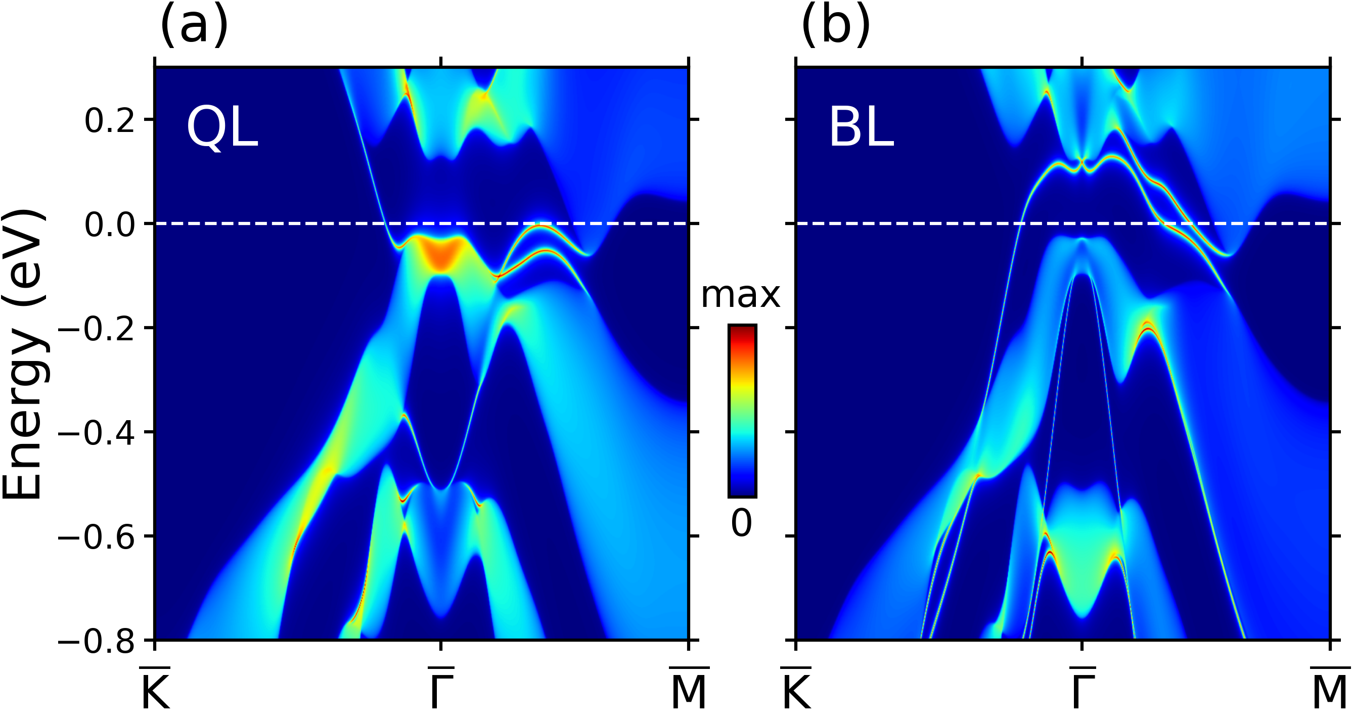
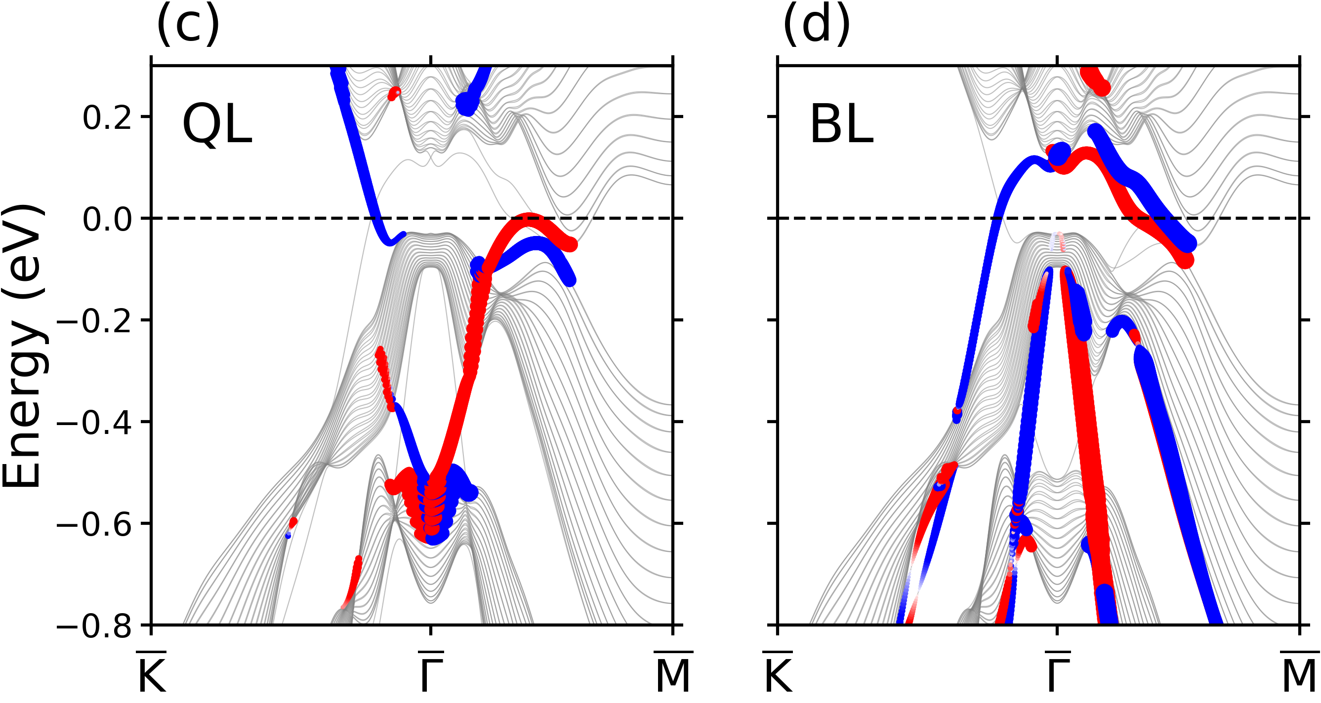
Due to a relatively weak coupling between the QLs and BLs, the (111) plane in the rhombohedral lattice [(001) plane in the hexagonal definition] is the surface with the lowest surface energy. The (111) cleavage plane induces either a QL or a BL surface termination. The TB parametrization of the -full band structure with the help of the Wannier functions has shown to be a very powerful tool to study surface states of topological materials [26]. Following this technique, in Fig. 5(a-b) we present electronic band structures for a semi-infinite film obtained with the iterative Green’s function method [40] as implemented in WannierTools [35]. The color code reflects the localization rate of the states at the topmost surface layer such that the bright narrow bands are the emerging surface states in each termination. Results are shown along the surface BZ path shown in Fig. 1, for both QL and BL terminations. Figs. 5 (c-d) present instead the -TB electronic surface structure for a finite slab [18 (QL+BL) layers]. As one can see from comparison of the semi-infinite and finite spectra, the 18 double-layer slab is sufficient to reproduce all details of the semi-infinite surface structure. This is in agreement with the conclusion of Ref. 41 that only a few layers are necessary to converge to the bulk behavior. The surface states with predominant localization on the lowest QL (c) and the topmost BL (d) in the slab are highlighted with circles whose size and color correspond to the magnitude and in-plane orientation (red for positive and blue for negative) of the spin-polarization perpendicular to the surface momentum.
The surface state dispersion patterns are remarkably distinct in both terminations. In the QL case, the surface states are dispersing upwards in energy when going away from the BZ center, whereas in the BL terminations the surface states have a downward dispersion. This behavior is in close resemblance to the behavior of the analogous studies in Bi1Te1 [13]. The surface states cross the Fermi level in both terminations, which already suggests a non-trivial topological nature of the material. Indeed, there is a single surface state crossing the Fermi level along the – path in both terminations. It is different along – where both states are located below the Fermi level in the QL termination, and crossing the Fermi level in the BL termination. It is important to point that only one surface state in the pair is connecting the VB and CB bulk bands and thus can be considered topologically non-trivial. Moreover, the topologically non-trivial band in the QL termination is approaching very closely to the Fermi level at its maximum along –. Disregarding that the bulk material still has a small density of states at the Fermi energy, Bi4Te3 reveals topological features distinctive for a strong topological material. Since the material crystal symmetry contains an inversion center, the topological invariants are readily calculated from the valence-state parities at the time-reversal-invariant momenta (TRIM) [4]. The parity invariants for each bulk TRIM () are shown in Fig. 1 where the colors of the red (blue) dots correspond to signs of the valence-state parity eigenvalue products = (). Based on the parity invariants, we obtain which characterizes Bi4Te3 as a strong topological material similar to Sb or Bi1-xSbx [42]. According to its , one expects an odd number of surface states crossing the Fermi level and the presence of an electron pocket surrounding , which is perfectly supported by our simulations. Our electronic band structure differs from the one presented in the Topological Materials Database of Ref. 14. As a consequence and in contrast to our findings, one would deduce from the data of Ref. 14, which would characterize Bi4Te3 as a weak topological material. Therefore, experimental studies are required to back up either of the theoretical predictions.
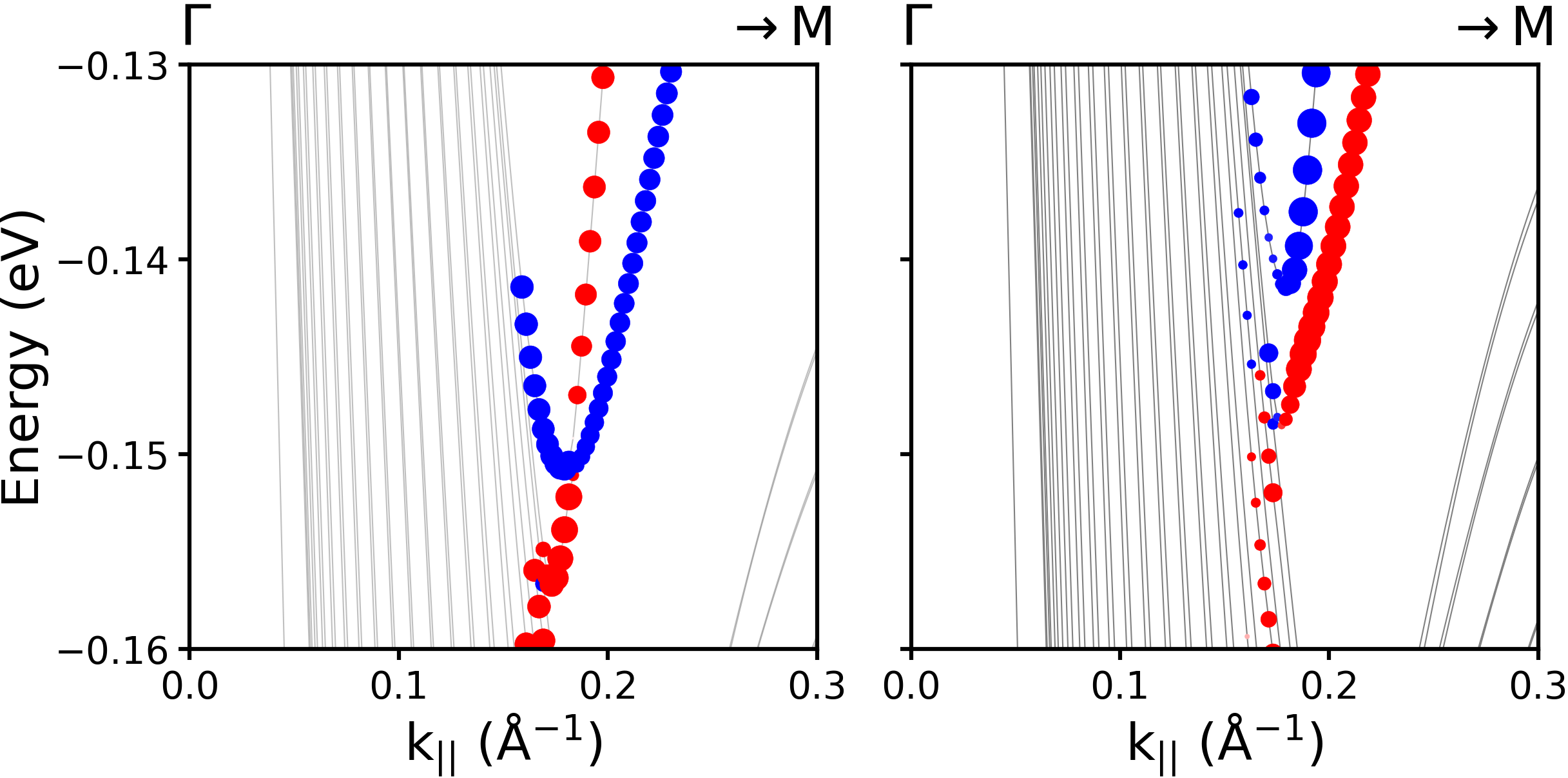
In addition to the mentioned behavior of the surface states, there are three important features that are revealed in Fig. 5. First, there is a crossing between a pair of surface states in the QL termination along –. The crossing is located at an energy of about eV in the close vicinity of the bulk state continuum. This feature has motivated us to study another topological invariant that characterizes the behavior of the surface states in the presence of mirror symmetry, the magnetic mirror Chern number [42, 5, 10]. The result confirms the existence of a single surface state which connects the valence and conduction bands and can potentially lead to a crossing of the two surface bands. The physical picture is similar to the analogous situation in Bi1-xSbx [42], where the same value of has been shown to be a marker of the band crossing. The mirror Chern number can have a non-zero value only if the crystal possesses a mirror plane. Therefore, as a check, we have slightly strained the crystal along the hexagonal axis and thus destroyed the mirror plane. In Fig. 6 we compare the behavior of the surface states in the vicinity of the discussed crossing point in the symmetric and deformed Bi4Te3 crystals. For demonstration purposes, we have computed the PBE surface band structures for 18 (QL+BL) layers slab. As it is seen from the left panel of Fig. 6, the crossing takes place at Å-1 in the crystal with the mirror plane. In the deformed crystal (right panel), the states are shifted with respect to each other such that no crossing occurs. An equivalent crossing has been observed in the surface states of Bi1Te1 along the same path and approximately at the same momentum [13].
The second feature to be discussed is a Dirac-cone like crossing located in the BL termination at at an energy of about 0.1 eV above the Fermi energy, slightly below the bulk conduction band minimum. The existence of this Dirac point for the BL termination can also be understood by looking at the system of one bilayer of Bi deposited on Bi2Te3 [12]. As in Bi/Bi2Te3, there seems to be a charge transfer from the BL to the QL. This shifts the Dirac cone above the Fermi level. There is one important consequence now in terms of the band crossing along -: Since the mirror Chern number is positive, the lowest of the two spin-split surface states connects the valence band to the conduction band [42]. When the Dirac point is below the Fermi level [QL case in Fig. 5(c)], there is a band crossing of the two surface states. When instead the Dirac cone is above the Fermi level [BL case in panel (d)], no crossing appears.
A third Dirac-cone feature comes from the Dirac cone of Bi2Te3. This can be seen as a Dirac cone crossing at below the Fermi level ( eV) for the QL termination. The Dirac cone seems to be resonant with the bulk continuum [Fig. 5(a)], and reveals itself better in Fig. 5(c) for the finite slab as a strongly spin-polarized feature.
VI Surface electronic structure by ARPES
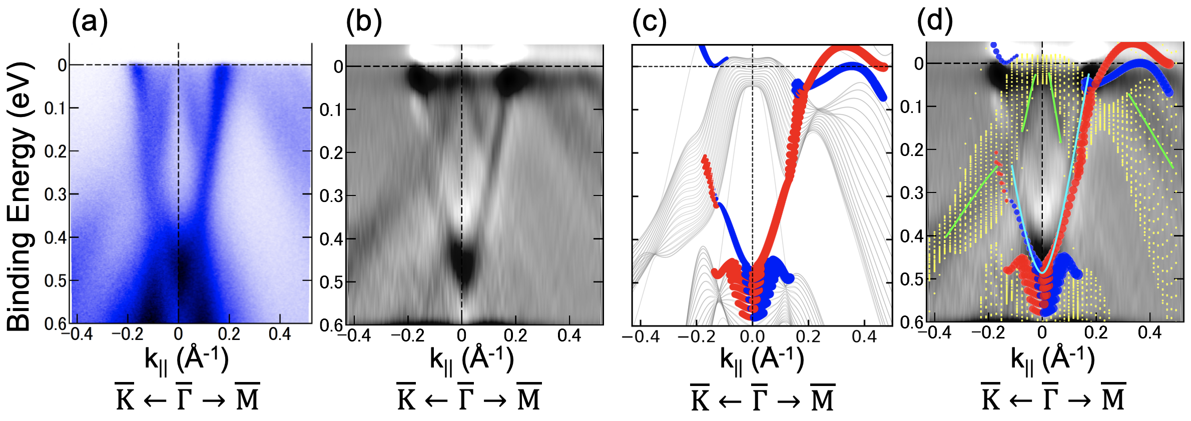
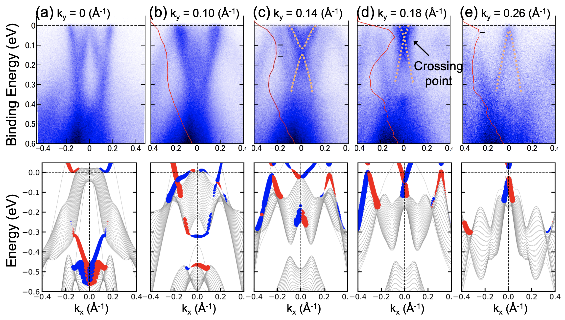
Figures 7(a) and (b) present the experimental spectrum of the QL terminated (111) surface of a thin-film of Bi4Te3 as measured by ARPES for two directions. For comparison with the experiment, theoretical bands have been shifted 50 meV upwards in Fig. 7(c). An overlay of the two electronic structures in Fig. 7(d) shows the very good agreement between the experimental and theoretical spectra. The comparison makes it possible to distinguish the features from the bulk-like states (yellow dots) and from the surface states (red and blue circles). Thus, the experimental bands marked with green lines in Fig. 7(d) correspond to bulk states. The sharp parabolic shape line (turquoise) is the surface state equivalent to the one that can be observed in Bi2Te3 [12] and Bi1Te1 [13]. Note that although this band disperses sharply all the way up to the Fermi level for the – direction, its intensity is weak along the – direction at 0.1-0.2 eV due to the strong hybridization with the bulk states. The experimental spectrum reveals also an additional band along – with a binding energy of meV. As indicated in the theoretical spectrum, this is the second surface state that crosses the parabolic-like surface state as it was discussed in Sec. V.2. This crossing is an important marker of the topological crystalline nature of Bi4Te3. To confirm that the crossing does take place, the ARPES spectra have been recorded along the non-symmetry lines along (parallel to –) for different values of as is sketched in Fig. 8 with red dashed lines. These spectra are shown and compared to the corresponding theoretical band structures in Fig. 9. As it follows from Figs. 9(c),(d), and (e), the Dirac cone crossing likely occurs around Å-1.
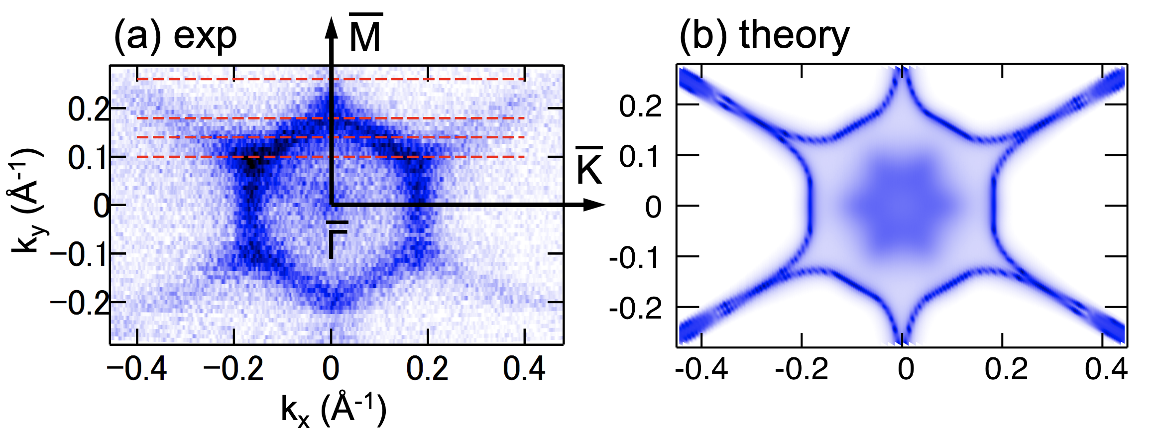
The Fermi surface of the thin-film Bi4Te3 shown in Fig. 8 has a hexagonal shape surrounding the point with straight branches going outwards at each corner. A similar shape is obtained in the -TB simulations. Sharp lines correspond to the crossing of the iso-energy surface with the surface states. The form of the Fermi surface is as expected from the classification [see, e.g., Fig. 6(a) of Ref. 42].
VII Summary
We have performed a combined theoretical and experimental study of the electronic structure of Bi4Te3. As its closely related compounds Bi2Te3 and Bi1Te1, Bi4Te3 is a dual topological material: a strong topological insulator with invariant equal to (1;111), and a topological crystalline insulator with mirror Chern number . The semimetallic groundstate predicted in DFT changes into a small indirect band gap semiconductor upon inclusion of the quasiparticle corrections in the framework of the approximation of many-body perturbation theory.
We discussed how inclusion of off-diagonal matrix elements of the electronic self-energy is important for capturing the fine details of the hybridization of states due to the strong spin-orbit coupling. This hybridization between many-body states is responsible for the gap opening in Bi4Te3.
Theoretical analysis of Bi4Te3 films reveals topologically non-trivial surface states. The presence and dispersion of these states are consistent with ARPES measurements of a QL terminated Bi4Te3 thin film. Both theory and experiment evidence a Dirac crossing between the surface states in the valence region. This crossing is attributed to the presence of a mirror symmetry and corresponding non-trivial value of the mirror Chern number.
Acknowledgements.
We gratefully acknowledge the computing time granted through JARA-HPC on the supercomputer JURECA at Forschungszentrum Jülich. M.T. acknowledges the kind hospitality of the Peter Grünberg Institut and Institute for Advanced Simulation, Forschungszentrum Jülich at the beginning of this project. Taisuke Sasaki and Kazuhiro Hono are acknowledged for their help in the TEM observation, and Kazuki Sumida, Kiyohisa Tanaka and Shin-ichiro Ideta are acknowledged for their help in the ARPES measurements. This work was supported by Grants-In-Aid from the JSPS KAKENHI (Grant No. 18H03877), the Murata Science Foundation (Grant No. H30084), the Asahi Glass Foundation, the Iketani Science and Technology Foundation (Grant No. 0321083-A), and a Tokyo Tech Challenging Research Award. The ARPES measurements were performed under UVSOR Proposals No. 19-569, and No. 19-858, and No. 20-777. D.N. and S.B. are supported by the European Centre of Excellence MaX “Materials design at the Exascale” (Grant No. 824143) funded by the EU. S.B. is grateful for financial support from the Deutsche Forschungsgemeinschaft (DFG) through the Collaborative Research Center SFB 1238 (Project C01).References
- Hasan and Kane [2010] M. Z. Hasan and C. L. Kane, Reviews of Modern Physics 82, 3045 (2010).
- Moore [2010] J. E. Moore, Nature 464, 194 (2010).
- Qi and Zhang [2011] X.-L. Qi and S.-C. Zhang, Reviews of Modern Physics 83, 1057 (2011).
- Fu and Kane [2007] L. Fu and C. L. Kane, Physical Review B 76, 045302 (2007).
- Fu [2011] L. Fu, Physical Review Letters 106, 106802 (2011).
- Hughes et al. [2011] T. L. Hughes, E. Prodan, and B. A. Bernevig, Physical Review B 83, 245132 (2011).
- Schindler et al. [2018] F. Schindler, A. M. Cook, M. G. Vergniory, Z. Wang, S. S. P. Parkin, B. A. Bernevig, and T. Neupert, Science Advances 4, eaat0346 (2018).
- Zhang et al. [2009] H. Zhang, C.-X. Liu, X.-L. Qi, X. Dai, Z. Fang, and S.-C. Zhang, Nature Physics 5, 438 (2009).
- Chen et al. [2009] Y. L. Chen, J. G. Analytis, J.-H. Chu, Z. K. Liu, S.-K. Mo, X. L. Qi, H. J. Zhang, D. H. Lu, X. Dai, Z. Fang, S. C. Zhang, I. R. Fisher, Z. Hussain, and Z.-X. Shen, Science 325, 178 (2009).
- Rauch et al. [2014] T. Rauch, M. Flieger, J. Henk, I. Mertig, and A. Ernst, Physical Review Letters 112, 016802 (2014).
- Belopolski et al. [2017] I. Belopolski, S.-Y. Xu, N. Koirala, C. Liu, G. Bian, V. N. Strocov, G. Chang, M. Neupane, N. Alidoust, D. Sanchez, H. Zheng, M. Brahlek, V. Rogalev, T. Kim, N. C. Plumb, C. Chen, F. Bertran, P. L. Fèvre, A. Taleb-Ibrahimi, M.-C. Asensio, M. Shi, H. Lin, M. Hoesch, S. Oh, and M. Z. Hasan, Science Advances 3, e1501692 (2017), https://www.science.org/doi/pdf/10.1126/sciadv.1501692 .
- Hirahara et al. [2011] T. Hirahara, G. Bihlmayer, Y. Sakamoto, M. Yamada, H. Miyazaki, S.-i. Kimura, S. Blügel, and S. Hasegawa, Physical Review Letters 107, 166801 (2011).
- Eschbach et al. [2017] M. Eschbach, M. Lanius, C. Niu, E. Młyńczak, P. Gospodarič, J. Kellner, P. Schüffelgen, M. Gehlmann, S. Döring, E. Neumann, M. Luysberg, G. Mussler, L. Plucinski, M. Morgenstern, D. Grützmacher, G. Bihlmayer, S. Blügel, and C. M. Schneider, Nature Communications 8, 14976 (2017).
- [14] https://www.topologicalquantumchemistry.com.
- Jeffries et al. [2011] J. R. Jeffries, A. L. Lima Sharma, P. A. Sharma, C. D. Spataru, S. K. McCall, J. D. Sugar, S. T. Weir, and Y. K. Vohra, Physical Review B 84, 092505 (2011).
- Saito et al. [2017] Y. Saito, P. Fons, K. Makino, K. V. Mitrofanov, F. Uesugi, M. Takeguchi, A. V. Kolobov, and J. Tominaga, Nanoscale 9, 15115 (2017).
- Kioupakis et al. [2010] E. Kioupakis, M. L. Tiago, and S. G. Louie, Phys. Rev. B 82, 245203 (2010).
- Yazyev et al. [2012] O. V. Yazyev, E. Kioupakis, J. E. Moore, and S. G. Louie, Phys. Rev. B 85, 161101(R) (2012).
- Nechaev et al. [2013] I. A. Nechaev, R. C. Hatch, M. Bianchi, D. Guan, C. Friedrich, I. Aguilera, J. L. Mi, B. B. Iversen, S. Blügel, P. Hofmann, and E. V. Chulkov, Phys. Rev. B 87, 121111(R) (2013).
- Aguilera et al. [2013a] I. Aguilera, C. Friedrich, G. Bihlmayer, and S. Blügel, Phys. Rev. B 88, 045206 (2013a).
- Nechaev and Chulkov [2013] I. A. Nechaev and E. V. Chulkov, Phys. Rev. B 88, 165135 (2013).
- Aguilera et al. [2013b] I. Aguilera, C. Friedrich, and S. Blügel, Physical Review B 88, 165136 (2013b).
- Rusinov et al. [2013] I. P. Rusinov, I. A. Nechaev, and E. V. Chulkov, JETP Letters 98, 397 (2013).
- Michiardi et al. [2014] M. Michiardi, I. Aguilera, M. Bianchi, V. E. de Carvalho, L. O. Ladeira, N. G. Teixeira, E. A. Soares, C. Friedrich, S. Blügel, and P. Hofmann, Physical Review B 90, 075105 (2014).
- Nechaev et al. [2015] I. A. Nechaev, I. Aguilera, V. De Renzi, A. di Bona, A. Lodi Rizzini, A. M. Mio, G. Nicotra, A. Politano, S. Scalese, Z. S. Aliev, M. B. Babanly, C. Friedrich, S. Blügel, and E. V. Chulkov, Phys. Rev. B 91, 245123 (2015).
- Aguilera et al. [2019] I. Aguilera, C. Friedrich, and S. Blügel, Physical Review B 100, 155147 (2019).
- Aguilera et al. [2015] I. Aguilera, C. Friedrich, and S. Blügel, Phys. Rev. B 91, 125129 (2015).
- Mostofi et al. [2008] A. A. Mostofi, J. R. Yates, Y.-S. Lee, I. Souza, D. Vanderbilt, and N. Marzari, Comput. Phys. Commun. 178, 685 (2008).
- Yamana et al. [1979] K. Yamana, K. Kihara, and T. Matsumoto, Acta Crystallographica Section B: Structural Crystallography and Crystal Chemistry 35, 147 (1979).
- [30] See Supplemental Material for further computational details.
- Friedrich et al. [2010] C. Friedrich, S. Blügel, and A. Schindlmayr, Physical Review B 81, 125102 (2010).
- [32] http://www.flapw.de.
- Perdew et al. [1996] J. P. Perdew, K. Burke, and M. Ernzerhof, Physical Review Letters 77, 3865 (1996).
- Li et al. [1990] C. Li, A. J. Freeman, H. J. F. Jansen, and C. L. Fu, Physical Review B 42, 5433 (1990).
- Wu et al. [2018] Q. Wu, S. Zhang, H.-F. Song, M. Troyer, and A. A. Soluyanov, Computer Physics Communications 224, 405 (2018).
- Pizzi et al. [2020] G. Pizzi, V. Vitale, R. Arita, S. Blügel, F. Freimuth, G. Géranton, M. Gibertini, D. Gresch, C. Johnson, T. Koretsune, J. Ibañez Azpiroz, H. Lee, J.-M. Lihm, D. Marchand, A. Marrazzo, Y. Mokrousov, J. I. Mustafa, Y. Nohara, Y. Nomura, L. Paulatto, S. Poncé, T. Ponweiser, J. Qiao, F. Thöle, S. S. Tsirkin, M. Wierzbowska, N. Marzari, D. Vanderbilt, I. Souza, A. A. Mostofi, and J. R. Yates, Journal of Physics: Condensed Matter 32, 165902 (2020).
- Wang et al. [2011] G. Wang, X.-G. Zhu, Y.-Y. Sun, Y.-Y. Li, T. Zhang, J. Wen, X. Chen, K. He, L.-L. Wang, X.-C. Ma, J.-F. Jia, S. B. Zhang, and Q.-K. Xue, Advanced Materials 23, 2929 (2011).
- Kusaka et al. [2021] S. Kusaka, T. Sasaki, K. Sumida, S. Ichinokura, S.-i. Ideta, K. Tanaka, K. Hono, and T. Hirahara, (2021), to be published.
- Kimura et al. [2010] S.-I. Kimura, T. Ito, M. Sakai, E. Nakamura, N. Kondo, T. Horigome, K. Hayashi, M. Hosaka, M. Katoh, T. Goto, T. Ejima, and K. Soda, Review of Scientific Instruments 81, 053104 (2010).
- Sancho et al. [1984] M. P. L. Sancho, J. M. L. Sancho, and J. Rubio, J. Phys. F: Met. Phys. 14, 1205 (1984).
- Chagas et al. [2020] T. Chagas, G. A. S. Ribeiro, P. H. R. Gonçalves, L. Calil, W. S. Silva, Â. Malachias, M. S. C. Mazzoni, and R. Magalhães-Paniago, Electronic Structure 2, 015002 (2020).
- Teo et al. [2008] J. C. Y. Teo, L. Fu, and C. L. Kane, Physical Review B 78, 045426 (2008).