Second-harmonic generation in germanium-on-insulator from visible to telecom wavelengths
Abstract
The second-order process underpins many important nonlinear optical applications in the field of classical and quantum optics. Generally, the process manifests itself only in a non-centrosymmetric dielectric medium via an anharmonic electron oscillation when driven by an intense optical field. Due to inversion symmetry, group-IV semiconductors like silicon (Si) and germanium (Ge) are traditionally not considered as ideal candidates for second-order nonlinear optics applications. Here, we report the experimental observation of the second-harmonic generation (SHG) in a Ge-on-insulator (GOI) sample under femtosecond optical pumping. Specially, we report the first-time measurement of the SHG signal from a GOI sample in the telecom S-band by pumping at nm.
I Introduction
The first observation of second-harmonic generation (SHG) by Franken et al. in 1961 Franken has always been considered as the foundation for the field of nonlinear optics. Nowadays, SHG has been widely applied in many important scientific applications such as ultra-short pulse measurements Kane ; Nomura and optical microscopy in biology Campagnola ; Chen1 . More recently, the attention on SHG has been significantly increasing in the realm of modern quantum optics using entangled photon pairs Brendel ; Dousse ; LiuJ , which can be generated by the reversed-SHG process, known as spontaneous parametric down-conversion (SPDC) Arnaut ; Walther ; Guo .
Unfortunately, such second-order nonlinear processes enabled by a finite susceptibility are normally prohibited in foundry compatible semiconductor materials like silicon (Si) and germanium (Ge) due to their centrosymmetric unit cell. Numerous schemes have been proposed to enhance the second-order nonlinearity in Si photonics. Examples include strain engineering of Si Jacobsen ; Cazzanelli , resonant excitation of crystalline Si nanoparticles Makarov , and application of an electric field to Si waveguides Timurdogan . In contrast, for Ge, there is only a theoretical prediction of the mid-infrared (MIR) SHG in a strained Ge waveguide Leonardis . Since Ge is already on the list of materials in the Si photonics foundry and has recently gained prominence for on-chip lasers Rong ; Petykiewicz ; Bao ; Qi ; Joo ; Kim and MIR waveguides Soref ; Kang . It is desirable to enable and enhance second-order nonlinear optical processes in Ge to widen the functionality of this important material.
In this Article, we demonstrate the experimental observation of SHG in visible and telecom S-band wavelengths from a germanium-on-insulator (GOI) sample. A tunable femtosecond pulsed laser was used to pump the sample from near-infrared (NIR) to MIR spectral ranges up to nm. Typical quadratic power dependence of the SHG signal was confirmed both in visible ( nm) and S-band ( nm) wavelengths. By systematically tuning the pump wavelength, we also observe that the SHG wavelength is always double the photon energies of the pump photons, further confirming the validity of our SHG signals. We believe that the underlying physics of this SHG in Ge could be explained by the surface effect induced by symmetry breaking at the material interface Hollering ; Heinz ; Chen . This result shows the potential to produce entangled photon pairs using SPDC in Ge that holds the promise to the realization of monolithic quantum photonic-integrated circuits (PICs). More importantly, our first experimental report on generating telecom photons via a nonlinear optical process will pave the way for NIR and MIR nonlinear optics applications in Si photonics.
II NONLINEAR OPTICAL CHARACTERIZATION
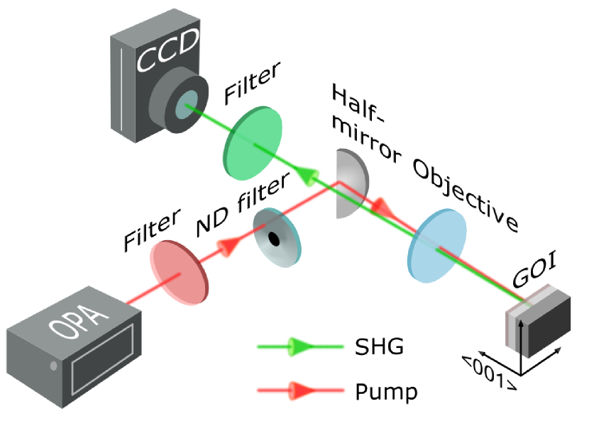
Our SHG experiments were performed in a home-built microscope spectroscopy setup, which is schematically depicted in Fig.1. Here, we used a femtosecond pulse optical parametric amplifier (OPA) with a repetition rate of 100 kHz as a tunable excitation pump. The OPA generated a tunable femtosecond laser pulses with wavelengths between to nm. Using the collinear nature of the OPA output, we carefully aligned and optimized the to nm pumps (red beam in Fig.1) by using its visible beam at nm as the reference optical path. To spectrally block the unwanted OPA idlers lower than the primary pump, optical filters were placed in front of the OPA output. A variable neutral density (ND) filter was used to attenuate the intense pump in the path. Then the attenuated optical beam was directed to an objective lens via a silver-coated half-mirror. We selected a reflective objective with a magnification and numerical aperture (NA) to focus the pump on the GOI sample. It allowed for both the optimal transmission of the pump from NIR to MIR and the collection of the SHG signal ranging from visible to telecom wavelengths. To measure the SHG spectra with a spectral resolution of nm, we used two separate D array detectors for visible and NIR spectrum measurement integrated on a spectrograph.
For this experimental study, we prepared a GOI sample, in which a Ge wafer is bonded to an oxidized Si substrate. The GOI was created using a direct wafer bonding technique Nam ; Nam2 ; Burt . The thickness of the GOI and the buried oxide layers were determined to be nm and nm, respectively, by using ellipsometry (not shown here).
III SECOND-HARMONIC GENERATION IN THE VISIBLE WAVELENGTHS
To demonstrate the mediated SHG in Ge samples, we first performed the real-time spectral measurement on the GOI using the setup shown in Fig.1. The OPA pump wavelength was initially set at nm, and its power onto the sample was adjusted to mW. Here, the photon energy of the excitation beam ( eV) is higher than the direct and indirect bandgap energies of Ge similar to the choice of the excitation pump used by Hollering et al Hollering . With the exposure time set to s for the visible CCD detector, a distinct SHG peak (green dots) centered at nm can be clearly observed on the spectrum in Fig.2. Next, we switched the OPA wavelength to and nm while maintaining the same power as the previous measurement. The SHG signals shifted correspondingly to (red dots) and nm (blue dots). The Gaussian fittings of the measured SHG were also plotted. Note that we carefully chose the measurement window to be centered at nm with a spectral width of nm for these measurements. A -nm short-pass filter was placed in front of the CCD to block the intense pump laser and its idler. To confirm that this signal at around nm is the SHG response in Ge, we carefully repeated the same test on a bare Si substrate, which did not show any signal with the same measurement parameters. It is worth noting that the same SHG response was observed in both bulk Ge and epitaxially grown Ge on Si, proving that the SHG is not exclusive to the GOI sample.
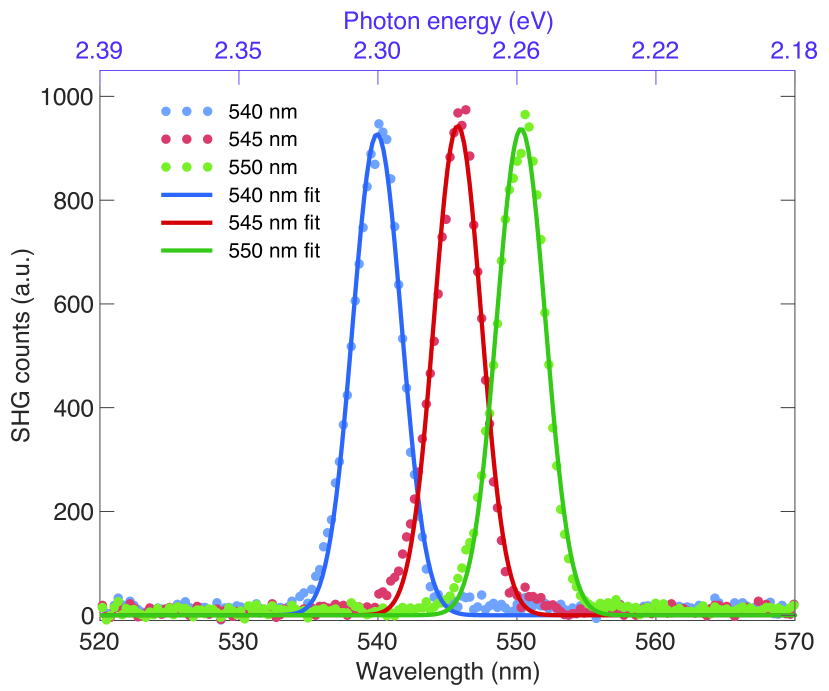
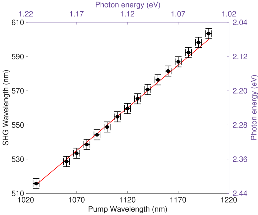
Figure 3 illustrates the measured SHG wavelength as a function of the pump wavelength. For this experiment, we linearly swept the OPA wavelength from to nm at a fixed power of mW, and captured the corresponding SHG spectra with a s exposure time. Then, we numerically extracted the SHG peak position by fitting the signal with a Gaussian profile. The top x-axis and right y-axis in purple in Fig.3 are the equivalent axes in photon energy. The error bars of nm were evaluated based on the spectrograph gratings and specifications of the OPA. There is a good agreement between the extracted data and the theoretical line in red, confirming the validity of the SHG.
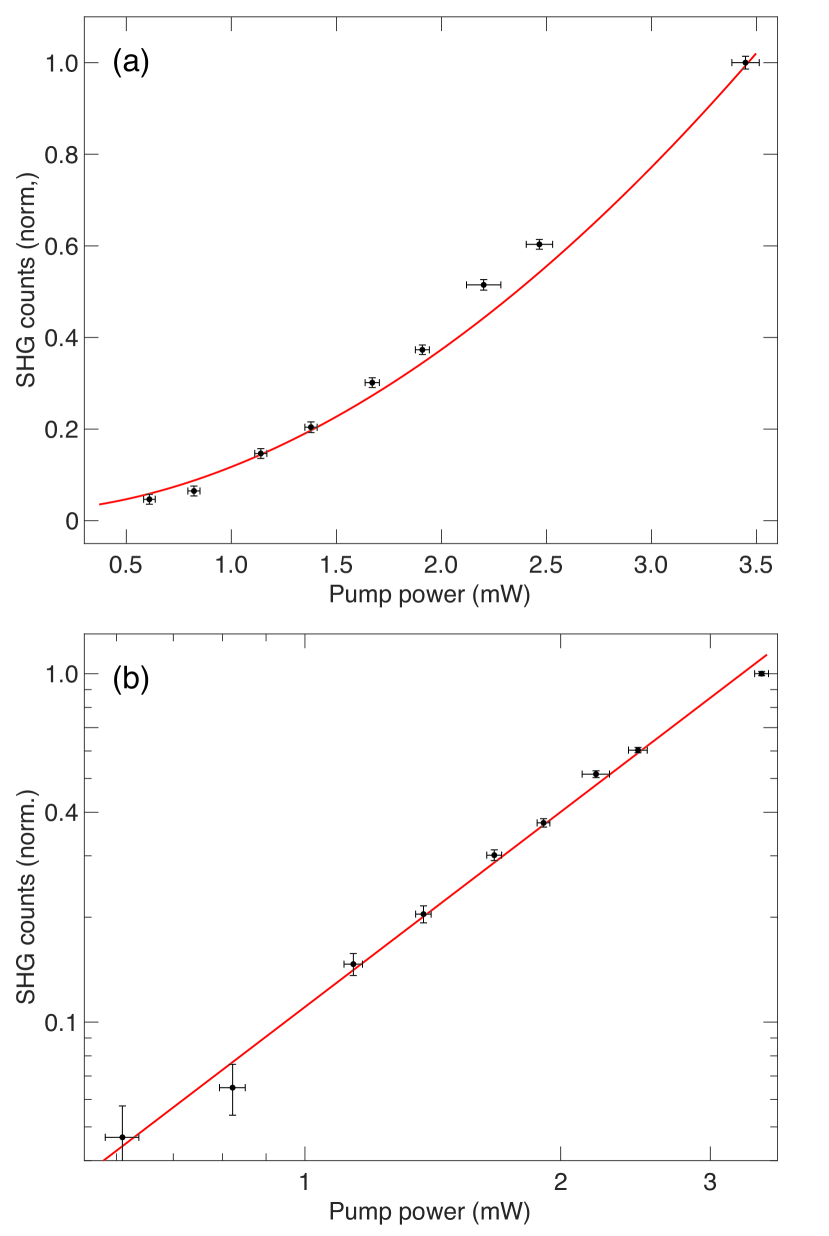
In Fig.4(a), we demonstrated the well-known signature of SHG in which the signal intensity follows a quadratic relationship with the excitation pump power Boyd . Here, by fixing the pump wavelength at nm, we linearly increased the pump power from to mW. The measured SHG signal (black dots) in the normalized counts exhibited a clear quadratic power dependence in Fig.4(a). The uncertainties (black error bars) in the pump power were determined by the standard deviation (SD) of a times repeated measurements at each pump power, and the errors in the SHG counts were estimated based on the calculated SD of the background signal noise with the same experimental settings. A second-order polynomial fitting with a confidence interval is displayed as the red curve. We also show the power law as a double logarithmic plot in Fig.4(b) Chen ; Timurdogan . These results demonstrate that the SHG measured in the GOI is in excellent agreement with the theory, with an estimated exponent of (red line).
IV SECOND-HARMONIC GENERATION IN THE TELECOM S-BAND
The GOI at room temperature typically displays a high intrinsic material absorptions between the visible to NIR with a cut-off wavelength around nm Stillman ; Gosciniak . For the SHG signal in the visible range enabled by the NIR pump (see Figs.2-4), the effect of the material absorption is inevitable. Hence, we decided to move the excitation pump into the MIR at a wavelength of nm, where the material absorption can be negligible for both pump and SHG. Since the pump photons have a much smaller energy than the bandgap energy of Ge, the electrons are only excited into virtual levels within the bandgap.
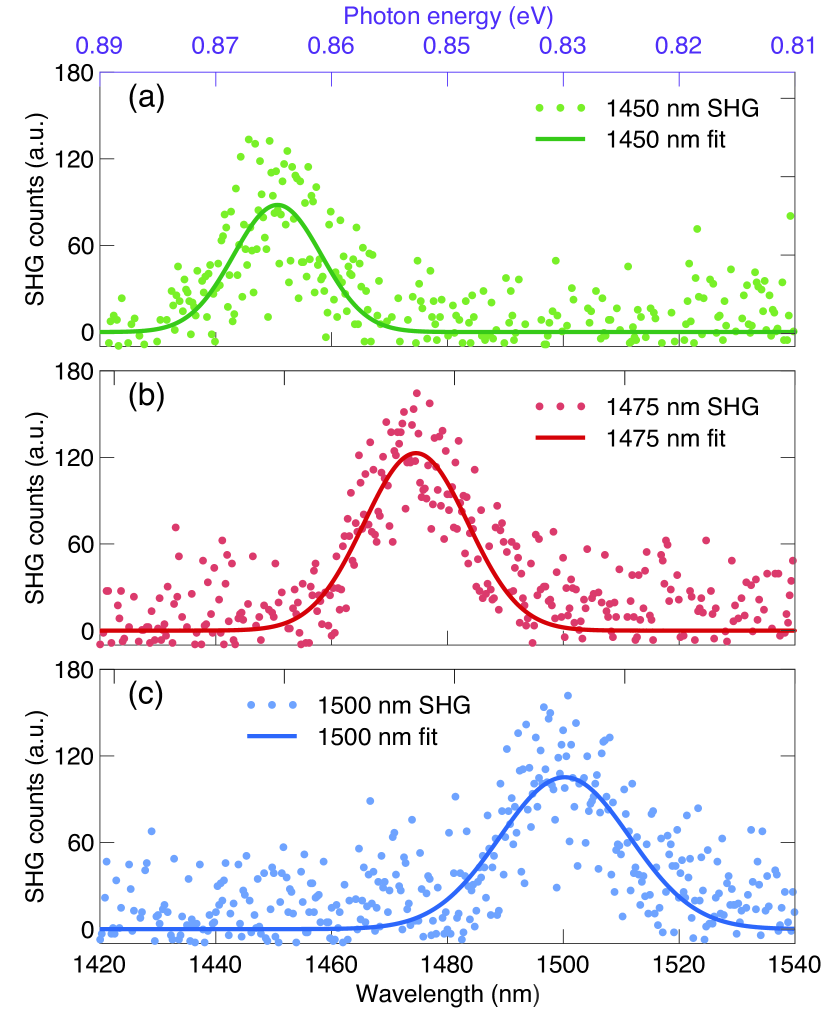
The optical setup for the MIR pumping is nearly the same as for the NIR pumping described in Fig.1. A -nm long-pass filter was placed at the OPA output to only transmit the desired pump photons at nm. First, with a -nm pump at mW and a CCD exposure time set at s, the SHG spectrum at nm was measured as the green dots shown in Fig.5(a). Subsequently, we increased the pump wavelength in a -nm increment, and plotted the corresponding SHG spectra at and nm in Figs.5(b) and (c), respectively. The SHG spectra at the telecom wavelength are spectrally noisier than that in the visible wavelength shown in Fig.2. This is accredited to the lower detection efficiency and higher dark currents of the InGaAs detector compared to the Si detector. We carefully confirmed the reproducibility of the SHG signals at the telecom S-band by repeating the same measurement at different areas on the GOI sample. To the best of our knowledge, this is the first experimental demonstration of the SHG signal in the technologically important telecom wavelength in Ge.
V Conclusion
To conclude, we reported the first experimental observation of the tunable SHG in a GOI sample ranging from visible to telecom wavelengths. We confirmed the validity of the SHG signals by studying the SHG wavelengths tuned by the pump wavelengths and also by presenting the characteristic quadratic power dependence. Whilst our current experimental setup has enabled the proof-of-principle SHG in Ge, there are a number of improvements that are left for future work. For example, we could improve the current setup to enable the SHG mapping on the Ge sample which potentially could provide more insights. We believe that our work paves the way toward developing nonlinear Si photonic devices operating in the telecom wavelengths.
Acknowledgements.
The research of the project was in part supported by Ministry of Education, Singapore, under grant AcRF TIER (RG /). The research of the project was also supported by Ministry of Education, Singapore, under grant AcRF TIER (MOE-T-- (S)). This work is also supported by National Research Foundation of Singapore through the Competitive Research Program (NRF-CRP--). This work is also supported by National Research Foundation of Singapore through the NRF-ANR Joint Grant (NRF-NRF-ANR TIGER). This work is also supported by the iGrant of Singapore A*STAR AME IRG (Ac). The authors would like to acknowledge and thank the Nanyang NanoFabrication Centre (NFC).Data Availability Statement
The data that support the findings of this study are available from the corresponding author upon reasonable request.
References
- (1) P. A. Franken, A. E. Hill, C. W. Peters, G. Weinreich, “Generation of Optical Harmonics,” Phys. Rev. Lett. 7, 118-119 (1961).
- (2) D. J. Kane, R. Trebino, “Characterization of arbitrary femtosecond pulses using frequency-resolved optical gating,” IEEE J. Quantum Electron. 29, 571-579 (1993).
- (3) Y. Nomura, H. Shirai, T. Fuji, “Frequency-resolved optical gating capable of carrier-envelope phase determination”, Nat. Commun. 4, 1-11 (2013).
- (4) P. J. Campagnola, A. C. Millard, M. Terasaki, P. E. Hoppe, C. J. Malone, W. A. Mohler “Three-dimensional high-resolution second-harmonic generation imaging of endogenous structural proteins in biological tissues,” Biophys. J. 82, 493-508 (2002).
- (5) X. Chen, O. Nadiarynkh, S. Plotnikov, P. J. Campagnola, “Second harmonic generation microscopy for quantitative analysis of collagen fibrillar structure,” Nat. Protoc. 7, 654-669 (2012).
- (6) J. Brendel, N. Gisin, W. Tittel, H. Zbinden, “Pulsed energy-time entangled twin-photon source for quantum communication,” Phys. Rev. Lett. 82, 2594 (1999).
- (7) A. Dousse, J. Suffczyński, A. Beveratos, O. Krebs, A. Lemaître, I. Sagnes, J. Bloch, P. Voisin, P. Senellart “Ultrabright source of entangled photon pairs,” Nature 466, 217–220 (2010).
- (8) J. Liu, R. Su, Y. Wei, B. Yao, S. Silva, Y. Yu, J. Smith, K. Srinivasan, A. Rastelli, J. Li, X. Wang. “A solid-state source of strongly entangled photon pairs with high brightness and indistinguishability,” Nat. Nanotechnol. 14, 586-93 (2019).
- (9) H. Arnaut, G. Barbosa, “Orbital and intrinsic angular momentum of single photons and entangled pairs of photons generated by parametric down-conversion,” Phys. Rev. Lett. 85, 286 (2000).
- (10) P. Walther, K. J. Resch, T. Rudolph, E. Schenck, H. Weinfurter, V. Vedral, M. Aspelmeyer, A. Zeilinger, “Experimental one-way quantum computing,” Nature 434, 169-176 (2005).
- (11) X. Guo, C. -L. Zou, C. Schuck, H. Jung, R. Cheng, H. X. Tang, “Parametric down-conversion photon-pair source on a nanophotonic chip,” Light Sci. Appl. 6, e16249-e16249 (2017).
- (12) R. S. Jacobsen, K. N. Andersen, P. I. Borel, J. Fage-Pedersen, L. H. Frandsen, O. Hansen, M. Kristensen, A. V. Lavrinenko, G. Moulin, H. Ou, C. Peucheret, B. Zsigri, A. Bjarklev, “Strained silicon as a new electro-optic material,” Nature 441, 199-202 (2006).
- (13) M. Cazzanelli, F. Bianco, E. Borga, G. Pucker, M. Ghulinyan, E. Degoli, E. Luppi, V. Véniard, S. Ossicini, D. Modotto, S. Wabnitz, R. Pierobon, L. Pavesi, “Second-harmonic generation in silicon waveguides strained by silicon nitride,” Nat. Mater. 11, 148-154 (2012).
- (14) S. V. Makarov, M. I. Petrov, U. Zywietz, V. Milichko, D. Zuev, N. Lopanitsyna, A. Kuksin, I. Mukhin, G. Zograf, E. Ubyivovk, “Efficient second-harmonic generation in nanocrystalline silicon nanoparticles,” Nano Lett. 17, 3047-3053 (2017).
- (15) E. Timurdogan, C. V. Poulton, M. J. Byrd, M. R. Watts, “Electric field-induced second-order nonlinear optical effects in silicon waveguides,” Nat. Photon. 11, 200-206 (2017).
- (16) F. De Leonardis, B. Troia, R. A. Soref, V. M. N. Passaro, “Investigation of mid-infrared second harmonic generation in strained germanium waveguides,” Opt. Express 24, 11126 (2016).
- (17) H. Rong, A. Liu, R. Jones, O. Cohen, D. Hak, R. Nicolaescu, A. Fang, M. Paniccia, “An all-silicon Raman laser,” Nature 433, 292-294 (2005).
- (18) J. Petykiewicz, D. Nam, D. Sukhdeo, S. Gupta, S. Buckley, A. Piggott, J. Vučković, K. Saraswat, “Direct bandgap light emission from strained Ge nanowire coupled with high-Q optical cavities,” Nano Lett. 16, 2168-2173 (2016).
- (19) S. Bao, D. Kim, C. Onwukaeme, S. Gupta, K. Saraswat, K. Lee, Y. Kim, D. Min, Y. Jung, H. Qiu, H. Wang, E. A. Fitzgerald, C. Tan, D. Nam, “Low-threshold optically pumped lasing in highly strained Ge nanowires,” Nat. Commun. 8, 1845 (2017) .
- (20) Z. Qi, H. Sun, M. Luo, Y. Jung, D. Nam, “Strained germanium nanowire optoelectronic devices for photonic-integrated circuits,” J. Condens. Matter Phys. 30, 334004 (2018).
- (21) H. Joo, Y. Kim, D. Burt, Y. Jung, L. Zhang, M. Chen, S. Parluhutan, D. Kang, C. Lee, S. Assali, O. Moutanabbir, Y. Cho, C. Tan, D. Nam,␣“1D photonic crystal direct bandgap GeSn-on-insulator laser,” Appl. Phys. Lett. 119, 201101 (2021).
- (22) Y. Kim, S. Assali, D. Burt, Y. Jung, H. Joo, M. Chen, D. Kang, Z. Ikonic, O. Moutanabbir and D. Nam, “Enhanced GeSn microdisk lasers directly released on Si,” Adv. Opt. Mater. 9, 2101213 (2021).
- (23) R. Soref, “Mid-infrared photonics in silicon and germanium,” Nat. Photon. 4, 495-497 (2010).
- (24) J. Kang, M. Takenaka, S. Takagi, “Novel Ge waveguide platform on Ge-on-insulator wafer for mid-infrared photonic integrated circuits,” Opt. Express 24, 11855-64 (2016).
- (25) C. K. Chen, A. R. B. De Castro, Y. R. Shen, “Surface-Enhanced Second-Harmonic Generation,” Phys. Rev. Lett. 46, 145-148 (1981).
- (26) T. F. Heinz, M. T. Loy, W. A. Thompson, “Study of Si() Surfaces by Optical Second-Harmonic Generation: Reconstruction and Surface Phase Transformation,” Phys. Rev. Lett. 54, 63-66 (1985).
- (27) R. W. J. Hollering, A. J. Hoeven, J. M. Lenssinck, “Optical second-harmonic generation study of Si and Ge deposition on Si(001),” J. Vac. Sci. Technol. 8, 3194-3197 (1990).
- (28) D. Nam, J. -H. Kang, M. L. Brongersma, K. C. Saraswat, “Observation of improved minority carrier lifetimes in high-quality Ge-on-insulator using time-resolved photoluminescence,” Opt. Lett. 39, 6205-6208 (2014).
- (29) D. Nam, D. Sukhdeo, S. Gupta, J. Kang, M. Brongersma, K. Saraswat, “Study of carrier statistics in uniaxially strained Ge for a low-threshold Ge laser,” IEEE J. Sel. Top. Quantum Electron. 20, 16-22 (2014).
- (30) D. Burt, H. Joo, Y. Jung, Y. Kim, M. Chen, Y. Huang, D. Nam,␣“Strain-relaxed GeSn-on-insulator (GeSnOI) microdisks,” Opt. Express 28, 28959-28967 (2021).
- (31) R. W. Boyd, “Nonlinear optics,” Academic press. 2020.
- (32) J. Gosciniak, M. Rasras, “High-bandwidth and high-responsivity waveguide-integrated plasmonic germanium photodetector,” J. Opt. Soc. Am. B 36, 2481 (2019).
- (33) G. E. Stillman, V. M. Robbins, N. Tabatabaie, “III-V compound semiconductor devices: Optical detectors,” IEEE Trans 31, 1643-1655 (1984).