Coexistence of Multiple Stacking Charge Density Waves in Kagome Superconductor
Abstract
The recently discovered Kagome family (A = K, Rb, Cs) exhibits rich physical phenomena, including non-trivial topological electronic structure, giant anomalous Hall effect, charge density waves (CDW) and superconductivity. Notably, CDW in is evidenced to intertwine with its superconductivity and topology, but its nature remains elusive. Here, we combine x-ray scattering experiments and density-functional theory calculations to investigate the CDWs in and demonstrate the coexistence of 2 2 2 and 2 2 4 CDW stacking phases. Competition between these CDW phases is revealed by tracking the temperature evolution of CDW intensities, which also manifests in different transition temperatures during warming- and cooling measurements. We also identify a meta-stable quenched state of after fast-cooling process. Our study demonstrates the coexistence of competing CDW stackings in , offering new insights in understanding the novel properties of this system.
Materials with kagome nets are promising candidates for quantum spin liquid S.Yan2011science ; 2016RevModPhys ; 2017RevModPhys and can support a variety of electronic orders like charge bond order, charge density wave (CDW) and unconventional superconductivityGuo.H.M.2009prb ; 2009prb.sc ; 2013prb.competing.Orders . Recently, a new class of kagome materials (A = K, Rb, Cs) has entered the scene and triggered a surge of research. These materials are found to be topological metals and show giant anomalous Hall conductivityprm2019Brenden ; Brenden.prl ; AHE.KVS ; AHE.CVS . More intriguingly, superconductivity transitions below 3 K were reported in Brenden.prl ; prm2021sc.KVS ; cpl2021RVS.sc . Above the superconducting transition temperature, a CDW phase transition ranging from 78 K to 103 K was also reported prm2019Brenden ; Brenden.prl ; cpl2021RVS.sc ; jiangyx . As in most unconventional superconductors, such as cuprates YBCO2012SCI ; YBCO2012natphy and pnictides BNCA2019PRL , the CDW in seems to compete with its superconductivity song2021CVS.thickness ; Qi2021pressure ; uniaxial2021prb ; RVS.pressure ; KVS.pressure . In addition, CDW in kagome lattice has been proposed to be a chiral flux phase, which breaks the time-reversal symmetry (TRS) without spin polarization and may be related to the anomalous Hall effect zhiweiWang.prb ; jiangyx ; AHE.CVS ; AHE.KVS ; yu2021flux ; xilinFeng2021 . This TRS breaking has been found to persist into the superconductivity state, indicating an intimate relation between charge order and unconventional superconductivity miuSR.nat . Additionally, the nematic susceptibility is observed to be enhanced below CDW transition temperature by elastoresistance measurements nematic.CDW.nat . Overall, these results indicate that the CDW in is intertwined with its superconductivity and topology in an intriguing way.
Of the family, has the highest superconducting transition temperature 2.5 K Brenden.prl . It also undergoes a CDW transition at 94 K with both in-plane and out-of-plane components, whose underlying mechanism remains elusive Brenden.prl ; H.X.Li.IXS.prx ; sdh2021Brenden . More strikingly, the superconducting phase diagram of shows a double-dome while the CDW phase is diminished by applying pressure or doping, indicating an unusual competition between CDW and superconductivity F.H.Yu.pressure.nc ; XuChen.pressure.cpl ; ChenKY.pressure.PRL ; doping.2sc . Regarding the in-plane CDW, while the inverse star of David (ISD) deformation is energetically favored according to first principles calculations and as confirmed by the observation of the Shubnikov-de Haas oscillation H.X.Tan.prl.calcu ; xilinFeng2021 ; sdH.prl.CVS , the star of David (SD) deformation is supported by nuclear quadrupole resonance measurements J.luo2021NMR . As for the out-of-plane component, in addition to the proposed 2 2 2 (2c) and 1 4 modulations H.X.Li.IXS.prx ; zhiweiWang.prb ; zuoweiLiang.prx ; jiangyx ; shumiya.prb.STM ; zhao.nat , non-resonant x-ray diffraction measurements on observed a unique 2 2 4 (4c) CDW phase appearing below 94 K sdh2021Brenden , which has not been reported in or . It is argued that there is only 4c CDW phase in sdh2021Brenden , which needs further experimental confirmation.
The 2c and/or 4c CDW phases may originate from different inter-layer stackings. The stacking degree of freedom in layered materials has been shown to be a powerful knob for manipulating physical properties. For example, in bilayer graphene, flat bands and superconductivity are induced by twisting two layers of non-superconducting graphene by a “magic angle” cao2018nat . In transition metal dichalcogenides, CDW stacking is considered to be important in determining the metal-insulator transition CDWstacking2000TaS2 ; TaS22016natcom . Therefore, it is important to investigate in detail the CDW phase(s) in , in order to understand the role it plays in various electronic properties in this material.
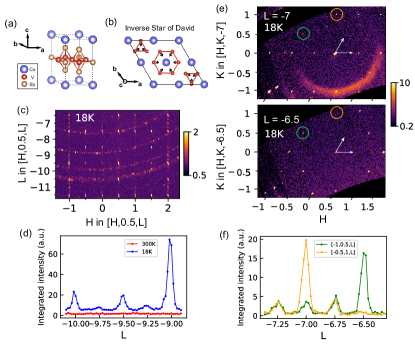
In this work, we use x-ray diffraction (XRD) and resonant x-ray scattering (REXS) techniques in conjunction with density-functional theory (DFT) calculations to study the CDW phases in . Based on the temperature evolution of diffraction peaks, we establish the coexistence of 2c and 4c CDW phases, with different transition temperatures. The observed spectral weight transfer between 2c and 4c diffraction peaks in warming and cooling processes signals a competition between these phases. In particular, the onset temperature of 4c on cooling ( 89 K) is found to be lower than the corresponding vanishing temperature on warming ( 92.8 K). An intriguing quenched state due to fast cooling is observed in the warming experiment, which could have critical implications in interpreting experimental anomalies at about 60 70 K 2symmetry2021natcom ; NLWang2021prb ; Qstahl2021 . By performing spatial mapping of CDW intensity using REXS, we observe that the different CDW modulations tend to exclude each other spatially further supporting the coexistence of different order parameters and competition between them. Comparison with computed diffraction patterns based on DFT calculations suggests the observed CDW structures arise from different stackings of ISD deformed V-containing layers. Our new results clarify the stacking CDWs in , which is very important in understanding and controlling the topological and superconducting properties in this material.
Single crystal x-ray diffraction measurements were performed using the custom-designed x-ray instrument equipped with a Xenocs Genix3D Mo (17.48 keV) x-ray source, which provides 2.5 photons/sec in a beam spot size of 150 at the sample position SI . Resonant x-ray scattering measurements were carried out at the beamline P09 at PETRA III, DESY (Hamburg, Germany) P09 . The single-crystalline samples for the present study were grown by a self-flux growth method SI .
The structure of in normal state VESTA is shown in FIG. 1(a), which is comprised of alternating layers of alkali-metal and . The vanadium atoms form a perfect kagome lattice under ambient conditions prm2019Brenden . After cooling from 300 K to 18 K (at a rate of 8 K/min), a cascade of CDW peaks becomes manifest at the half-integer plane, as shown in Figure 1(c-d). Diffraction peaks are labeled by their Miller indices, , of the undistorted high-temperature phase. The CDW peaks are about 3 orders of magnitude weaker than the main Bragg peaks, indicating small lattice distortions. The x-ray diffraction pattern was indexed according to a hexagonal unit cell with lattice parameters 5.53 Å and 9.28 Å SI . The observed CDW peaks can be classified into three categories, namely, q1, q2 and q3-type peaks corresponding to integer, half-integer and quarter-integer values, respectively. For a CDW reflection, either or or both are half-integers owing to the in-plane reconstruction jiangyx ; zhiweiWang.prb .
It is worth mentioning that we have not detected any reflection with a quarter integer or , suggesting the absence of cell quadrupling along or , which is consistent with previous XRD measurements li2021spatial . Thus, our results obtained with a highly sensitive two-dimensional detector further confirm that the 1 4 modulation observed by several STM experiments may not be a bulk effect li2021spatial ; zhiweiWang.prb ; zhao.nat . We also notice that symmetry is broken at low temperatures, consistent with previous works Qstahl2021 . Because the CDW peaks at q = [] and [] are equivalent in symmetry, however, as shown in Figure 1(e, f), they differ greatly in intensity at 18 K. Either ISD [shown in Figure 1(b)], SD distortion or order of orbital current would preserve symmetry in kagome plane. However, for a 3D CDW, the phase shift of adjacent kagome layers breaks the symmetry xilinFeng2021 ; miao2021geometry ; H.X.Tan.prl.calcu . One recent measurement of polar Kerr rotation of has reported the formation of two-fold rotation symmetry below 94 K NLWang.TRS .
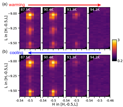
To further elucidate the origin of q1, q2 and q3-type CDW peaks, we select the CDW peaks at q1 = [-0.5,-0.5,-9], q2 = [-0.5,-0.5,-9.5] and q3 = [-0.5,-0.5,-9.25] and trace their evolutions across transition temperatures SI . As shown in Fig. 2, the intensities of CDW peaks at q1 and q2 gradually descend with increasing temperatures and then abruptly drop to zero above 94 K. Intriguingly, the q3-type CDW peak disappears at 93 K, about 1 K lower than that of q1 and q2-CDWs. Surprisingly, in the cooling process, while q1 and q2-type CDW peaks promptly emerge below 94 K, the appearance of q3-type CDW peak lags until further cooling below 89K.
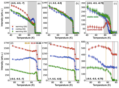
This thermal hysteresis of q3-type CDW peak is unexpected. As further verification, the sample was subjected to multiple thermal cycling, during which the intensities of CDW peaks were recorded in situ, as shown in Fig. 3. The first warming process was measured after a fast cooling from room temperature to 18 K at a rate of K/min (red curve). The measurements at each temperature point were repeated six times and summed together for better statistics. The scanning time for each temperature point was around 1.5 hours. After warming up to 105 K, we proceeded to the cool down measurement under the same conditions (blue curve), so that CDW was allowed to evolve quasi-statically. Then we performed a second warming measurement (green curve). We have tracked three CDW peaks considering their relatively strong intensity within our measured reciprocal space, indexed by [-0.5, -0.5, 7], [-1, 0.5, -6.5] and [-0.5, -0.5, -6.75] respectively. From these results we have identified a quenched-state (QS) of CDW in as a consequence of the fast-cooling process, which is evidenced by the discrepancy between the two warming processes (red and green curves). In fact, our experiments revealed that even a freezing rate of 2 K/min was too fast for the 4c CDW to establish completely, and the system would settle in a meta-stable quenched-state with weak -type CDW signals at low temperature SI . On the other hand, a quasi-static cooling process could drive the 4c CDW into a coherent stable-state (SS) with much high intensity of q3-type CDW at low temperature.
For the first warming process (referred as QS), the q3-type CDW peak is greatly enhanced above 75 K as shown in Fig. 3(c). We note that another XRD study reported the appearance of q3-type CDW peak above a similar temperature scale of 60 K upon warming Qstahl2021 . However, instead of the coexistence of q1, q2 and q3-type CDW peaks at 18 K that we observed, they found no signals of q3-type CDW peak below 60 K and argued that 4c CDW was a super-cooled phase Qstahl2021 . However, we found that the intensity of the q3-type CDW was even stronger after quasi-static cooling, ruling out that possibility. Most intriguingly, as shown in Figure 3(d)-(f), we can identify three characteristic temperatures, i.e. 93.8 K for the onset of q1 and q2-type CDW peaks, 92.8 K for the onset of q3-type CDW peaks during warming process, and 89 K for the onset of q3-type CDW peaks during the cooling process. These multiple transition temperatures are contradicting the previous claim that the different modulations observed in CsV3Sb5 would originate from a unique stacking of 2 2 4. The sharp transitions and hysteresis temperature behavior suggest that the CDW transitions are first-order transitions, consistent with other experiments Qstahl2021 ; J.luo2021NMR ; Noah2021prm ; NLWang2021prb .
Moreover, our results suggest a competition between 2c and 4c CDW phases. For example, in the cooling process upon the formation of the 4c CDW phase below 89 K, the intensities of CDWs at [-0.5, -0.5, 7] and [-1, 0.5, -6.5] are suppressed after 89 K [see blue curves in Figure 3 and direct comparisons in ref. SI ]. That is to say, the onset temperature of 4c CDW at 89 K changes the intensity of q1 and q2-CDWs from a peak to a dip. This behavior is more pronounced in the former. We speculate this is due to the different relative contributions of 2c and 4c CDWs in q1 and q2-type CDW peaks, since the structure factors contribute differently in reciprocal space. A similar competition effect was observed in the warming process, where the disappearance of the 4c CDW phase above 92.8 K led to a peak in the intensity of CDWs at [-0.5, -0.5, 7] and [-1, 0.5, -6.5] [see green curves in Figure 3].
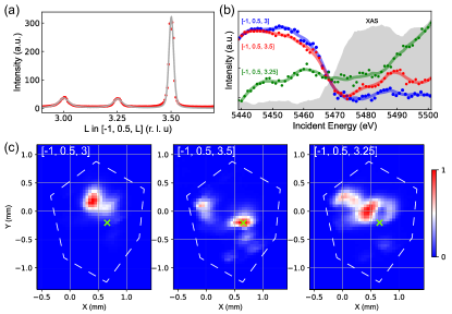
The nature of the CDW phase is further elucidated using REXS at V -edge. We selected three CDW peaks at q1 = [-1, 0.5, 3], q2 = [-1, 0.5, 3.5] and q3 = [-1, 0.5, 3.25] (see Fig. 4(a)) to study their energy dependence. As shown in Fig. 4(b), we observed a dip at V -edge for all three CDW peaks. This is similar to the energy dependence of the 2 2 2 CDW in , which originates from lattice displacement in CDW phase TiSe2_PRR . Then we performed a spatial mapping of the intensity of the three CDW peaks at 5465 eV as shown in Fig. 4(c). Intriguingly, the q1, q2 and q3-CDWs seem to exclude each other spatially, rendering a single-phase scenario unlikely.
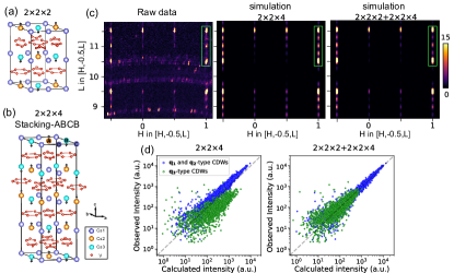
Comparison with simulated diffraction patterns lends support for the coexistence of 2c and 4c stacking CDW phases in . Our DFT optimization produces three types of 3D CDW structures with approximately the same energy (within 1 meV per formula unit), including one 2c CDW and two 4c CDW SI . All structures have identical in-plane ISD deformation and differ in the stackings of V-containing layers. There are 4 translationally inequivalent Cs sites in a supercell, denoted A, B, C, D as shown in Figure 5, and an ISD deformed V-layer is called X-stacked (X=A,B,C,D) if its contracting V-hexagon sits on the X-sites. In our DFT calculations, the SD deformation is found to be unstable and transforms spontaneously into ISD deformation when neighboring V-layers are differently stacked H.X.Tan.prl.calcu . The stable CDW structures are the 2c supercell with AB stacking (see Fig.5(a)) and the 4c supercells with ABCB (see Fig.5(b)) and ABCD stacking SI . Structural optimization shows that a contracting V-hexagon pulls the neighboring Cs ions toward itself. The frustration of a Cs atom in identifying with the two adjacent V layers then favors alternating stacking of the V hexagons, leading to various possible stackings.
We then fit the experimental XRD results as an incoherent superposition of the intensity of calculated CDW structures. Since symmetry can be broken by the stacking, we consider the equivalents (three for each) in the fittings. It was argued that all CDW superlattice peaks originated from a single stacking of 4c phase sdh2021Brenden . Thus, we first simulated the XRD patterns considering only 4c structures, including three equivalent ABCB sequences and three equivalent ABCD sequences [more information in ref. SI ]. Figure 5(c) shows representative simulation patterns. The fitting with only the 4c structures is clearly inadequate with exaggerated q3-type peaks (correlation coefficient 0.80 for CDW peaks), which can be improved by including both 4c and 2c stackings in the model (correlation coefficient 0.91 for CDW peaks), as is evident from the correlation maps shown in Figure 5(d). In other words, a reasonable fit of our data is only achieved from the coexistence of 2c and 4c structures. Inclusion of the 2 2 1 (1c) CDW with ISD deformation in the model produces little improvement SI . Notably, the proposed 4c CDW structure with modulation between ISD and SD distortions sdh2021Brenden is inconsistent with our XRD data SI .
In summary, through systematic temperature-dependent XRD measurements, we discover the coexistence and competition of 2c and 4c CDW phases in through different transition temperatures. Scanning REXS show that these modulations tend to exclude each other spatially. In conjunction with DFT calculation, our diffraction measurements reveal the microscopic origin of 2c and 4c CDW structures arising from different stackings of the “inverse star of David” structures. These results provide critical insights into the underlying CDW instability in and offer a possible explanation to understand the double-peak behavior of by applying pressure or doping on F.H.Yu.pressure.nc ; ChenKY.pressure.PRL ; doping.2sc . The first peak of may be due to the completed destruction of one stacking phase while the disappearance of both stacking CDW phases leads to the second peak of . Our results reveal that the coexistent 2c and 4c CDWs are close in free energy, so external perturbations can effectively modulate the CDW phases to tune the related exotic properties. This establishes as an exciting new platform for manipulating electronic properties.
Acknowledgements.
Y. Y. P. is grateful for financial support from the Ministry of Science and Technology of China (2019YFA0308401 and 2021YFA1401903) and the National Natural Science Foundation of China (11974029). J.F. acknowledges the financial support from the National Natural Science Foundation of China (11725415 and 11934001), the Ministry of Science and Technology of China (2018YFA0305601) and the National Key R&D Program of China (2021YFA1400100). Y. F. Guo acknowledges the financial support from the National Science Foundation of China (Grant No. 92065201). We acknowledge DESY (Hamburg, Germany), a member of the Helmholtz Association HGF, for the provision of experimental facilities. Parts of this research were carried out at beamline P09 at PETRA III. Beamtime was allocated for proposal I-20220028. We acknowledge Dr. P. Bereciartua for helping with the REXS experimental control.References
- (1) Yan, S., Huse, D. A. & White, S. R. Spin-Liquid Ground State of the = 1/2 Kagome Heisenberg Antiferromagnet. Science 332, 1173–1176 (2011).
- (2) Norman, M. R. Colloquium: Herbertsmithite and the search for the quantum spin liquid. Rev. Mod. Phys. 88, 041002 (2016).
- (3) Zhou, Y., Kanoda, K. & Ng, T.-K. Quantum spin liquid states. Rev. Mod. Phys. 89, 025003 (2017).
- (4) Guo, H.-M. & Franz, M. Topological insulator on the kagome lattice. Phys. Rev. B 80, 113102 (2009).
- (5) Ko, W.-H., Lee, P. A. & Wen, X.-G. Doped kagome system as exotic superconductor. Phys. Rev. B 79, 214502 (2009).
- (6) Wang, W.-S., Li, Z.-Z., Xiang, Y.-Y. & Wang, Q.-H. Competing electronic orders on kagome lattices at van hove filling. Phys. Rev. B 87, 115135 (2013).
- (7) Ortiz, B. R. et al. New kagome prototype materials: discovery of , and . Phys. Rev. Materials 3, 094407 (2019).
- (8) Ortiz, B. R. et al. : A Topological Kagome Metal with a Superconducting Ground State. Phys. Rev. Lett. 125, 247002 (2020).
- (9) Yang, S.-Y. et al. Giant, unconventional anomalous Hall effect in the metallic frustrated magnet candidate, . Science Advances 6, eabb6003 (2020).
- (10) Yu, F. H. et al. Concurrence of anomalous hall effect and charge density wave in a superconducting topological kagome metal. Phys. Rev. B 104, L041103 (2021).
- (11) Ortiz, B. R. et al. Superconductivity in the kagome metal . Phys. Rev. Materials 5, 034801 (2021).
- (12) Yin, Q. et al. Superconductivity and Normal-State Properties of Kagome Metal Single Crystals. Chinese Physics Letters 38, 037403 (2021).
- (13) Jiang, Y.-X. et al. Unconventional chiral charge order in kagome superconductor . Nature Materials 20, 1353–1357 (2021).
- (14) Ghiringhelli, G. et al. Long-Range Incommensurate Charge Fluctuations in (Y, Nd) Ba2Cu3O6+ x . Science 337, 821–825 (2012).
- (15) Chang, J. et al. Direct observation of competition between superconductivity and charge density wave order in . Nature Physics 8, 871–876 (2012).
- (16) Lee, S. et al. Unconventional Charge Density Wave Order in the Pnictide Superconductor . Phys. Rev. Lett. 122, 147601 (2019).
- (17) Song, Y. et al. Competition of Superconductivity and Charge Density Wave in Selective Oxidized Thin Flakes. Phys. Rev. Lett. 127, 237001 (2021).
- (18) Wang, Q. et al. Charge Density Wave Orders and Enhanced Superconductivity under Pressure in the Kagome Metal . Advanced Materials 33, 2102813 (2021).
- (19) Qian, T. et al. Revealing the competition between charge density wave and superconductivity in through uniaxial strain. Phys. Rev. B 104, 144506 (2021).
- (20) Wang, N. N. et al. Competition between charge-density-wave and superconductivity in the kagome metal . Phys. Rev. Research 3, 043018 (2021).
- (21) Du, F. et al. Pressure-induced double superconducting domes and charge instability in the kagome metal . Phys. Rev. B 103, L220504 (2021).
- (22) Wang, Z. et al. Electronic nature of chiral charge order in the kagome superconductor . Phys. Rev. B 104, 075148 (2021).
- (23) Yu, L. et al. Evidence of a hidden flux phase in the topological kagome metal . eprint arXiv:2107.10714.
- (24) Feng, X., Jiang, K., Wang, Z. & Hu, J. Chiral flux phase in the Kagome superconductor . Science Bulletin 66, 1384–1388 (2021).
- (25) Mielke, C. et al. Time-reversal symmetry-breaking charge order in a kagome superconductor. Nature 602, 245–250 (2022).
- (26) Nie, L. et al. Charge-density-wave-driven electronic nematicity in a kagome superconductor. Nature 604, 59–64 (2022).
- (27) Li, H. et al. Observation of Unconventional Charge Density Wave without Acoustic Phonon Anomaly in Kagome Superconductors (, Cs). Phys. Rev. X 11, 031050 (2021).
- (28) Ortiz, B. R. et al. Fermi Surface Mapping and the Nature of Charge-Density-Wave Order in the Kagome Superconductor . Phys. Rev. X 11, 041030 (2021).
- (29) Yu, F. H. et al. Unusual competition of superconductivity and charge-density-wave state in a compressed topological kagome metal. Nature Communications 12, 3645 (2021).
- (30) Chen, X. et al. Highly Robust Reentrant Superconductivity in under Pressure. Chinese Physics Letters 38, 057402 (2021).
- (31) Chen, K. Y. et al. Double Superconducting Dome and Triple Enhancement of in the Kagome Superconductor under High Pressure. Phys. Rev. Lett. 126, 247001 (2021).
- (32) Oey, Y. M. et al. Fermi level tuning and double-dome superconductivity in the kagome metal . Phys. Rev. Materials 6, L041801 (2022).
- (33) Tan, H., Liu, Y., Wang, Z. & Yan, B. Charge density waves and electronic properties of superconducting kagome metals. Phys. Rev. Lett. 127, 046401 (2021).
- (34) Fu, Y. et al. Quantum Transport Evidence of Topological Band Structures of Kagome Superconductor . Phys. Rev. Lett. 127, 207002 (2021).
- (35) Luo, J. et al. Possible star-of-David pattern charge density wave with additional modulation in the kagome superconductor . npj Quantum Materials 7, 30 (2022).
- (36) Liang, Z. et al. Three-Dimensional Charge Density Wave and Surface-Dependent Vortex-Core States in a Kagome Superconductor . Phys. Rev. X 11, 031026 (2021).
- (37) Shumiya, N. et al. Intrinsic nature of chiral charge order in the kagome superconductor . Phys. Rev. B 104, 035131 (2021).
- (38) Zhao, H. et al. Cascade of correlated electron states in the kagome superconductor . Nature 599, 216–221 (2021).
- (39) Cao, Y. et al. Unconventional superconductivity in magic-angle graphene superlattices. Nature 556, 43–50 (2018).
- (40) Influence of CDW stacking disorder on metal–insulator transition in 1T-TaS2. Solid State Communications 116, 47–50 (2000).
- (41) Ma, L. et al. A metallic mosaic phase and the origin of Mott-insulating state in 1T-TaS2. Nature Communications 7, 10956 (2016).
- (42) Momma, K. & Izumi, F. VESTA3 for three-dimensional visualization of crystal, volumetric and morphology data. Journal of Applied Crystallography 44, 1272–1276 (2011).
- (43) Xiang, Y. et al. Twofold symmetry of c-axis resistivity in topological kagome superconductor with in-plane rotating magnetic field. Nature Communications 12, 6727 (2021).
- (44) Wang, Z. X. et al. Unconventional charge density wave and photoinduced lattice symmetry change in the kagome metal probed by time-resolved spectroscopy. Phys. Rev. B 104, 165110 (2021).
- (45) Stahl, Q. et al. Temperature-driven reorganization of electronic order in . Phys. Rev. B 105, 195136 (2022).
- (46) See Supplementary Material at…for more information about crystal synthesis, experimental details, temperature dependence of beryllium, origin of diffuse scattering signals in XRD pattern, density-functional theory calculations and fitting of experimental data.
- (47) Strempfer, J. et al. Resonant scattering and diffraction beamline P09 at PETRA III. Journal of Synchrotron Radiation 20, 541–549 (2013).
- (48) Li, H. et al. Discovery of conjoined charge density waves in the kagome superconductor . Nature Communications 13, 6348 (2022).
- (49) Miao, H. et al. Geometry of the charge density wave in the kagome metal . Phys. Rev. B 104, 195132 (2021).
- (50) Wu, Q. et al. Simultaneous formation of two-fold rotation symmetry with charge order in the kagome superconductor by optical polarization rotation measurement. Phys. Rev. B 106, 205109 (2022).
- (51) Ratcliff, N., Hallett, L., Ortiz, B. R., Wilson, S. D. & Harter, J. W. Coherent phonon spectroscopy and interlayer modulation of charge density wave order in the kagome metal . Phys. Rev. Materials 5, L111801 (2021).
- (52) Peng, Y. et al. Observation of orbital order in the van der Waals material . Phys. Rev. Research 4, 033053 (2022).