Relating spin-polarized STM imaging and inelastic neutron scattering in the van-der-Waals ferromagnet \ceFe3GeTe2
Abstract
Van-der-Waals (vdW) ferromagnets have enabled the development of heterostructures assembled from exfoliated monolayers with spintronics functionalities, making it important to understand and ultimately tune their magnetic properties at the microscopic level. Information about the magnetic properties of these systems comes so far largely from macroscopic techniques, with little being known about the microscopic magnetic properties. Here, we combine spin-polarized scanning tunneling microscopy and quasi-particle interference imaging with neutron scattering to establish the magnetic and electronic properties of the metallic vdW ferromagnet . By imaging domain walls at the atomic scale, we can relate the domain wall width to the exchange interaction and magnetic anisotropy extracted from the magnon dispersion as measured in inelastic neutron scattering, with excellent agreement between the two techniques. From comparison with Density Functional Theory calculations we can assign the quasi-particle interference to be dominated by spin-majority bands. We find a dimensional dichotomy of the bands at the Fermi energy: bands of minority character are predominantly two-dimensional in character, whereas the bands of majority character are three-dimensional. We expect that this will enable new design principles for spintronics devices.
I Introduction
The discovery of ferromagnetic van-der-Waals (vdW) materials has enabled the possibility of manufacturing spintronics devices from vdW heterostructures He et al. (2021). Although, according to the Mermin-Wagner theorem, ferromagnetism should be unstable in two dimensions, recently a number of materials, including \ceFe3GeTe2, have been shown to exhibit ferromagnetism down to the monolayer limit Gong et al. (2017); Huang et al. (2017); Fei et al. (2018). The evolution of its magnetic order from 3D to 2D is an interesting open question Deng et al. (2018). The study of magnetic properties in 2D materials and at surfaces, however, is challenging. Conventional methods used to establish magnetic order parameters, such as neutron scattering, are not suitable for monolayer-thin samples and surfaces. Here, we use spin-polarised STM, quasiparticle interference imaging and neutron scattering to elucidate the interplay between the bulk and surface magnetic order and the low energy electronic structure of a quasi-2D ferromagnet. We identify two types of defects arising predominantly from Fe and Te vacancies, and show that quasiparticle scattering from these defects produces magnetic scattering dominated by the more two-dimensional electronic bands around the Fermi level. Imaging of a domain wall and comparison of its profile with the exchange coupling and magnetic anisotropy obtained from inelastic neutron scattering of bulk \ceFe_3GeTe_2 reveals good agreement, with evidence for a larger magnetic anisotropy and smaller exchange coupling in the surface layer.
II Results
II.1 Sample characterization
Fe3GeTe2 has a layered crystal structure with weak interlayer interactions and becomes ferromagnetic below Deiseroth et al. (2006). The material typically comes with an off-stoichiometry, where the iron concentration deviates from three due to vacancies and interstitial iron. The magnetic properties vary with the excess iron concentration May et al. (2016). Previous STM and ARPES investigations have been interpreted as Kondo-lattice-like behaviour Zhang et al. (2018). The material cleaves easily between the \ceFe_3-yGeTe2 layers, exhibiting a Te-terminated surface. We have used single crystal neutron diffraction to determine the crystal structure and in particular the exact stoichiometry of our samples, revealing an iron deficiency (see suppl. section I).
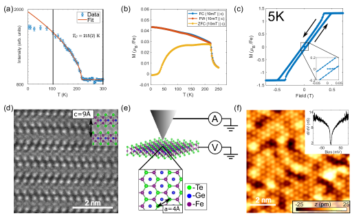
Magnetic characterisation (Fig. 1(a, b)) reveals a behaviour in field-cooled measurements consistent between the neutron scattering intensity of the Bragg peak and magnetisation, as well as with previous reports Tian et al. (2019). We find the magnetic transition at about and a suppression of magnetisation for zero-field cooled measurements starting below , Fig. 1(b), indicating stabilization of a domain structure which results in zero net magnetisation. In measurements of the magnetization as a function of field , shown in Fig. 1(c), we find magnetic hysteresis, as expected for a ferromagnet.
Cross-sectional TEM images (Fig. 1(d)) show the stacking sequence as expected from the crystal structure and the high quality of the samples, confirming the AB layer stacking. This type of stacking results in a Rashba-like band crossing at the K point and leads to the formation of topological line nodes Kim et al. (2018).
Fig. 1(e) shows the measurement set up for the STM measurement and expected surface termination. Topographic imaging of the \ceFe3GeTe2 surface (Fig. 1(f)) reveals a hexagonal lattice which can be attributed to the uppermost \ceTe lattice. The surface further exhibits a pronounced electronic inhomogeneity, which likely originates from the off-stoichiometry of the sample due to the iron deficiency. STS spectra show a pronounced gap around the Fermi level (inset of Fig. 1(f)).
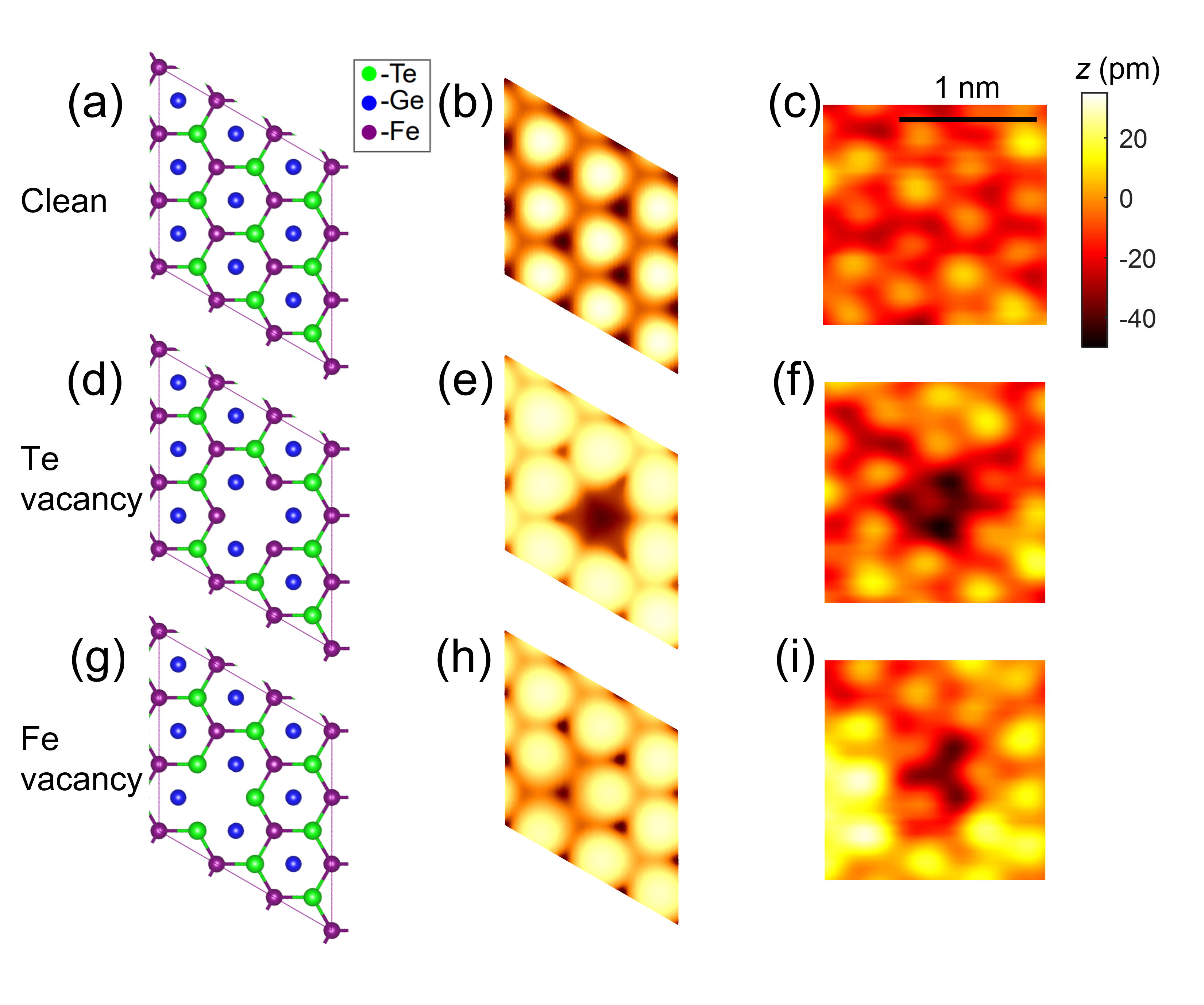
To gain a better understanding of the inhomogeneity in our topographic images, we have simulated STM images for different types of defects. Fig. 2 shows DFT calculations and measured topographic images for the clean surface and two types of defects, an iron vacancy and a tellurium vacancy. Comparison of the DFT calculations with the STM image for the clean surface (Fig. 2(a)-(c)) suggests that the atomic corrugation in the STM images is due to the surface tellurium lattice. A vacancy of a tellurium atom (as indicated in Fig. 2(d)) results in a clear triangular-like defect (Fig. 2(e)) which can be easily identified in the topographic image (Fig. 2(f)). An Fe-vacancy, shown in Fig. 2(g), produces a more subtle depression of the local density of states, as shown in Fig. 2(h), which can nevertheless be easily identified in our STM topographies (Fig. 2(i)). This depression in the density of states is likely responsible for the inhomogeneity in topographic images as shown in Fig. 1(b), and has been shown to be responsible for the lowering in as a function of Fe deficiencyMay et al. (2016). Interestingly, within our ferromagnetic DFT calculations for a monolayer of \ceFe3GeTe2 in a supercell, we find that the total magnetic moment per Fe atom is reduced by the presence of a defect (2.004 /Fe vs. 2.123 /Fe without a defect, see the method section for details).
II.2 Magnetic properties from STM and neutron scattering
We have studied the magnetism in \ceFe3GeTe2 using neutron scattering and spin-polarized STM to establish a better understanding of its magnetic properties, and the effect of the vacuum interface which will become more important in the 2D limit.
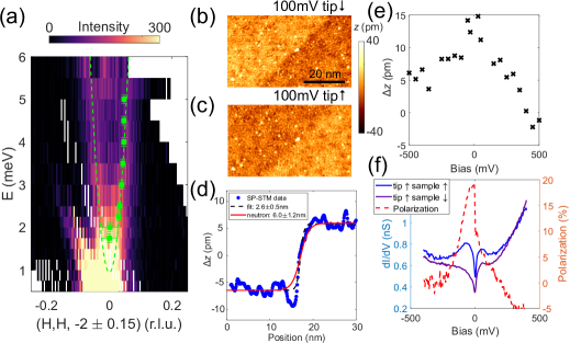
Fig. 3(a) shows the inelastic neutron data obtained from a single crystal, with a clear magnon dispersion in a cut through the peak starting from about . At long wavelengths, the magnetic excitations of an itinerant ferromagnet are well-described by a model of localized magnetic moments Lovesey (1984). To describe the spin wave dispersion in \ceFe3GeTe2 at small , we use an effective two-dimensional model of interacting Fe3+ ions on a honeycomb lattice with an easy-axis anisotropy,
| (1) |
Here, is the nearest neighbour interaction, the magnetic anisotropy, is the spin operator acting on site or and the vectors , and span between the unit cells containing nearest neighbor spins (in the space group). We have neglected further nearest neighbors since their effect in the limit of small is a simple renormalization of the spin-wave velocity and anisotropy gap. The eigenvalues obtained from the model are , with and , where is the spin Owerre (2016); Pershoguba et al. (2018). With a wavevector of , where is here used to parametrize the reciprocal lattice vector, the dispersion is quadratic for small , . We have fit Gaussian peaks to a series of constant energy cuts in the plane through the MACS data to obtain the magnon dispersion. The exchange coupling can be determined from the prefactor, , of the quadratic term. Taking the reduced value of , the fit yields meV and meV. The magnetic anisotropy is non-negligible, consistent with previous reports Deng et al. (2018); Tan et al. (2018), though somewhat smaller than the one reported previously from neutron scattering, whereas the exchange coupling is larger Calder et al. (2019). The difference in these values suggests a strong influence of the iron deficiency on the magnetic excitations: while our crystal has , the one studied in Ref. Calder et al., 2019 had , almost twice that of our sample.
We can compare these values with the magnetic properties of the surface layer. Using spin-polarized STMWiesendanger (2009); Bode (2003) we were able to directly image ferromagnetic domain walls at the surface of \ceFe3GeTe2 (Fig. 3(a)).
The tip cluster was found to have a sufficiently small moment so that the tip magnetisation can be switched by the magnetic interaction with the sample. Manipulating the tip magnetisation in this way allowed us to image the same area with an oppositely polarized tip without having to apply an external magnetic field which would at the same time move the domain wall and polarize the sample. Fig. 3(c) shows an image with the same tip after the tip magnetisation has flipped. By taking the difference of the images, we obtain an image of only the magnetic contrast (Fig. 3(d)). From a line profile normal to the domain wall (Fig. 3(d)), we can analyze its width by fitting to the data Moreno et al. (2016); Aharoni (2000); Berbil-Bautista
et al. (2007); Ravlić
et al. (2003); Wiesendanger (2009), assuming that the tip magnetization is parallel to the out-of-plane direction and reverses by when changing its direction. We obtain a domain wall width of . The domain wall width found here is smaller than that typically found in ferromagnetic films which are usually on the order of Berbil-Bautista
et al. (2007); Ravlić
et al. (2003). We can compare the domain wall width with the expected width using the exchange interaction and magnetic anisotropy obtained from neutron scattering through Blundell (2001), where is the exchange stiffness of the spins of the system being considered which is related to the exchange interaction . For a 2D hexagonal honeycomb lattice, this expression becomes Moreno et al. (2016); Aharoni (2000) (see supplementary section S4), where is the nearest neighbour distance between \ceFe atoms. By taking the values of and determined from the magnon dispersion in Fig. 3(a), we find a domain wall width which is somewhat larger than what is obtained from a fit to our spin-polarized STM measurement (see fig. 3(d)). We note, however, that visually, the domain wall profile suggested by neutron scattering appears very similar to the observed one. The smaller domain wall width which we observe at the surface suggests that the exchange coupling is smaller in the surface layer compared to the bulk, and the magnetic anisotropy larger.
The apparent height of the domain wall in the spin polarized STM images exhibits a strong dependence on the bias voltage. From images recorded at different bias voltages, we can determine how the spin polarization of the sample’s electronic structure evolves with energy. For images recorded with a low bias voltage () the domain wall shows the largest contrast. As the bias voltage is increased the magnetic contrast decreases and disappears at before reversing at even higher bias values. For negative applied bias the magnetic contrast remains more or less constant. By recording STS spectra on either side of the domain wall (hence with different magnetization directions of the sample) with a set point condition where the domain wall is not visible it is possible to extract the spin polarization as a function of bias voltage. The spectra recorded on either side of the domain wall are shown in Fig. 3(f). The polarization can be extracted from the spectra using the relation Bode (2003); Wiesendanger (2009) (Fig. 3(f)). The spin polarization shows a sharp peak of up to spin polarization just below the Fermi level at an energy of .
II.3 Quasi-particle interference
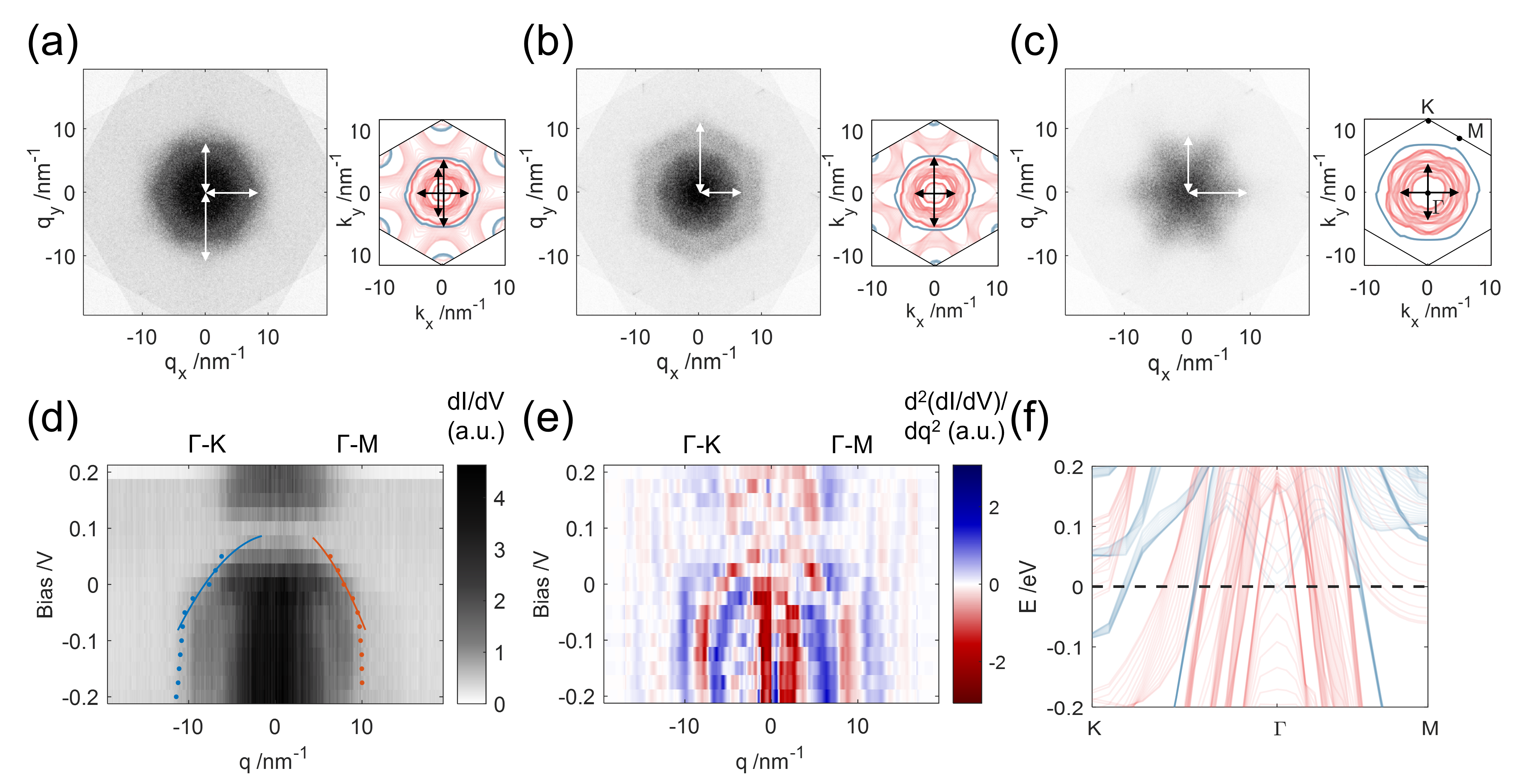
To characterize the interplay between magnetism and the electronic structure, we have used quasi-particle interference imaging. Fig. 4(a)-(c) show the Fourier transform of quasi-particle interference maps at three different bias voltages (, and ), with the calculated band structure in the first Brillouin zone for comparison, integrated over . There are clear hexagonal features in the experimental data, marked with arrows, with equivalent scattering vectors shown in the calculated band structure. All of the vectors observed experimentally can be assigned to scattering processes between bands with majority spin character. These bands are also the ones which exhibit a more two-dimensional character, as represented by the opacity in the calculation. Despite being strongly two-dimensional, the minority band centred around the point is not visible in any of our measurements. The DFT calculations show that the spin-minority bands have predominantly iron character with little weight on the outer-most Te atoms, whereas the majority bands have Te character, suggesting that we fail to detect the minority band due to matrix element effects.
A cut of the differential conductance along K--M in the 2D Brillouin zone is shown in Fig. 4(d) between and . From the QPI cuts we can extract the properties of the hole-like band that crosses the Fermi level. By fitting a parabolic dispersion, Fig. 4(d), and assuming that it is due to intra-band scattering we determine that it has an effective mass and a Fermi wavevector along ( in q-space) which is in approximate agreement with that of a hexagonal pocket centered around seen in ARPES measurements Kim et al. (2018); Zhang et al. (2018); Xu et al. (2020). From the fits we find a band maximum at above the Fermi level. To highlight sharp features, the second derivative with respect to of the smoothed dI/dV data is plotted in Fig. 4(e). In these, the hole band is more readily observed with a maximum at around at the point. We assign this band to the two-dimensional band at the same energy in the calculated -integrated band structure, Fig. 4(f).
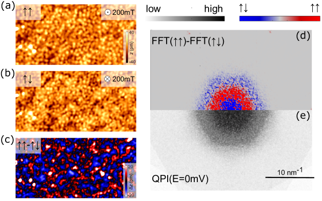
Using a spin-polarized tip allows to determine the spin character of the different bands. To this end, we have undertaken spin-polarized topographic imaging as a function of applied field. The relative orientation of the tip and sample magnetizations will switch at different fields (see Fig. 5(a-c)), enabling imaging of the quasi-particle scattering with parallel and anti-parallel alignment of their magnetizations. We observe a significant change in the topographic contrast when the tip and sample are not magnetized in the same direction anymore. Taking the difference of the Fourier transforms of topographies with parallel and antiparallel magnetization (Fig. 5(d)) reveals strong changes in the relative intensity of the scattering vectors. By comparing the Fourier transform with the quasi particle interference mapping at the Fermi level (Fig. 5(e)) we determine that the observed magnetic contrast is due to the spin-dependent imaging of Friedel oscillations between differently polarized bands at the Fermi level and thus reveals information about the spin polarization of the bands in the vicinity of the Fermi energy.
III Discussion
Our study of \ceFe3GeTe2 provides new insights from relating microscopic information obtained from low temperature scanning tunneling microscopy to bulk properties obtained from neutron scattering. We find that in the surface layer, the magnetic properties deviate slightly from those in the bulk, as might be expected from the 3D nature of some parts of the electronic structure. Comparison of the imaging of domain walls with the magnetic exchange interaction and anisotropy obtained from neutron scattering reveal a surprisingly good agreement. One would expect the ratio to be slightly larger for the surface layer compared to the bulk due to a larger magnetic anisotropy and smaller exchange coupling: the smaller coordination number of atoms in the surface layer will lead to a decreased exchange energy , while at the same time the lower symmetry is expected to result in a larger anisotropy . It is well known from a number of systems that the magnetic anisotropy increases with reduced dimensionality Gambardella (2003). The reduction in in the surface layer is consistent with the lower Curie temperature found in thin films and in the monolayer limit, where is suppressed significantly Deng et al. (2018); Fei et al. (2018). This system therefore confirms the previously observed trend that while the surface of a magnetic bulk material does not exhibit radically different magnetic properties, there are subtle differences Trainer et al. (2021).
From band structure calculations, we find that the Fermi surface is dominated by bands of spin majority character with significant -dispersion and quasi-2D bands of spin minority character. A comparison with quasi-particle interference imaging reveals dominant wave vectors which are broadly consistent with the band structure calculations. We use spin-polarized imaging to determine the spin-polarization of the bands near the Fermi energy, and find, consistent with the calculations, a hexagonal ring of scattering which we attribute to the bands with spin-majority character embedded in a rather broad distribution of electronic states with opposite spin character.
IV Acknowledgments
CT and PW acknowledge funding through EP/R031924/1 and EP/T031441/1, LCR through the Royal Commission for the Exhibition of 1851, IB through the International Max Planck Research School for Chemistry and Physics of Quantum Materials, and HL through the ISIS facility development studentship programme. Access to MACS was provided by the Center for High Resolution Neutron Scattering, a partnership between the National Institute of Standards and Technology and the National Science Foundation under Agreement No. DMR-1508249.
Author contributions: CT, ORA and IB carried out STM measurements, CT and ORA analyzed the STM data. HL and CT derived the expressions for the domain wall width and profile. LCR performed DFT calculations. HL, EC, JARR and CS undertook neutron measurements and crystal growth. PW and CS initiated and led the project. All authors contributed to and discussed the manuscript.
Corresponding author
Correspondence should be sent to P. Wahl (wahl@st-andrews.ac.uk).
Competing interests: The authors declare no competing financial interests.
Data Availability: Underpinning data will be made available at http://DOI to repository will be provided upon acceptance.
V Methods
V.1 Scanning Tunneling Microscopy
Scanning Tunneling Microscopy (STM) measurements were undertaken using two home-built STMs White et al. (2011); Trainer et al. (2017) operating at temperatures down to in cryogenic vacuum. Samples are cleaved at a temperature of before inserting them in to the STM head. The spin-polarized STM tips used in this study were prepared using two methods: the first method involved collecting magnetic material from the surface of a sample of an \ceFe_1+xTe sample Singh et al. (2015); Enayat et al. (2014) before inserting the \ceFe3GeTe2 into the STM. The second method involved picking up ferromagnetic material directly from the \ceFe3GeTe2 surface.
V.2 Crystal growth
Single crystals of \ceFe3GeTe2 were synthesized using the chemical vapor transport technique. Sealed quartz ampoules with an outer diameter of 18 mm and inner diameter of 16 mm were loaded with iron, germanium, and tellurium in stoichiometric quantities. Approximately 10mg of Iodine was loaded as a transport agent. The iron, germanium, and tellurium powder was initially pumped to 10 using a turbo pump to ensure dryness before the iodine was loaded. The combined reagents were then chilled and pumped to using an oil-based mechanical pump to avoid damage to the blades of the turbo pump. The tubes were sealed to be a length of and put into a 3-zone furnace such that one end was at and the other at . A chiller was used to further cool one end of the furnace to increase the temperature gradient. The temperature gradient was initially inverted for 12 hours to clean one end of the ampoules. The ampoules were then removed at high temperature with one end cooled using compressed air on removal from the three-zone furnace. The growth resulted in a variety of crystal sizes up to a maximum of the lateral size of , with a thickness of up to .
V.3 Neutron scattering
Neutron scattering measurements were performed on the MACS cold triple axis spectrometer (NIST, Gaithersburg) Rodriguez et al. (2008). Single crystals of \ceFe3GeTe2 with varying size were edge-aligned on aluminum plates, using the hexagonal morphology as a guide. A coating of hydrogen-free Fomblin oil was applied to the crystals to attach them to the mount and prevent degradation in air. The sample mount was positioned such that the (HHL) reflections lay in the horizontal scattering plane. The sample was then cooled to in a Orange Cryostat. was fixed to by 20 PG(002) double bounce analyzers and was varied between and by a vertically focused PG(002) monochromator, giving access to energy transfers between and . Cooled \ceBeO filters were placed on the scattered side of the sample to remove contamination from higher order scattering. This experimental configuration allowed for an energy resolution of approximately (FWHM) at the elastic line. A two-dimensional map of the scattering intensity along was constructed by integrating over in a window about (Fig. 3(a)).
The single-crystal neutron diffraction experiment was performed on hot neutron four-circle diffractometer D9, at ILL Chris et al. . Cu(220) incident-beam monochromator selected a wavelength Å, allowing measurements of Bragg peaks at high momentum transfer. A single-crystal of \ceFe3GeTe2 of approximate dimensions was characterized at four temperatures: (paramagnetic phase), , and (ferromagnetic phase). The refinement of nuclear and magnetic structure was performed using Fullprof Rodríguez-Carvajal (1993) giving an iron stoichiometry (from data), and a ferromagnetic moment at . Further details on the refinement are provided in the Supplementary Material.
V.4 DFT calculations
DFT calculations to simulate STM images of defects were performed using the Density Functional Theory package Quantum Espresso using Projected Augmented Wavefunctions (PAW) and the PBE exchange-correlation functional. We took a supercell of a monolayer of \ceFe3GeTe2 with vacuum and removed an atom to generate the defect. We then performed structural relaxations on the ferromagnetic 3x3 supercells until the total force was less than and the total energy change was less than . For the structural optimisation we used a -grid of . The kinetic energy cutoff was for the wavefunctions and for the charge density. Using these relaxed structural parameters we then performed a self consistent calculation using a denser k-grid of . The total magnetic moment was found to be /Fe for the supercell without a defect, /Fe with a Te defect and /Fe with an Fe defect. Finally, the local density of states was obtained using a -grid of for a bias setpoint of () and the STM image at constant current was generated using the CRITIC2 software de-la Roza et al. (2014). For calculations of the bulk electronic structure we used a kinetic energy cutoff of for the wavefunctions and for the charge density with a -grid of .
References
- He et al. (2021) J. He, S. Li, A. Bandyopadhyay, and T. Frauenheim, ACS NANO LETTERS 21, 3237 (2021), URL https://doi.org/10.1021/acs.nanolett.1c00520.
- Gong et al. (2017) C. Gong, L. Li, Z. Li, H. Ji, A. Stern, Y. Xia, T. Cao, W. Bao, C. Wang, Y. Wang, et al., Nature 546, 265 (2017), ISSN 1476-4687, URL https://doi.org/10.1038/nature22060.
- Huang et al. (2017) B. Huang, G. Clark, E. Navarro-Moratalla, D. R. Klein, R. Cheng, K. L. Seyler, D. Zhong, E. Schmidgall, M. A. McGuire, D. H. Cobden, et al., Nature 546, 270 (2017), ISSN 1476-4687, URL https://doi.org/10.1038/nature22391.
- Fei et al. (2018) Z. Fei, B. Huang, P. Malinowski, W. Wang, T. Song, J. Sanchez, W. Yao, D. Xiao, X. Zhu, A. F. May, et al., Nat. Mater. 17, 778 (2018), URL https://doi.org/10.1038/s41563-018-0149-7.
- Deng et al. (2018) Y. Deng, Y. Yu, Y. Song, J. Zhang, N. Z. Wang, Z. Sun, Y. Yi, Y. Z. Wu, S. Wu, J. Zhu, et al., Nature 563, 94 (2018), ISSN 1476-4687, URL https://doi.org/10.1038/s41586-018-0626-9.
- Deiseroth et al. (2006) H.-J. Deiseroth, K. Aleksandrov, C. Reiner, L. Kienle, and R. K. Kremer, European Journal of Inorganic Chemistry 2006 (2006), ISSN 1099-0682, URL https://onlinelibrary.wiley.com/doi/abs/10.1002/ejic.200501020.
- May et al. (2016) A. F. May, S. Calder, C. Cantoni, H. Cao, and M. A. McGuire, Phys. Rev. B 93, 014411 (2016), ISSN 2469-9950, 2469-9969, URL https://link.aps.org/doi/10.1103/PhysRevB.93.014411.
- Zhang et al. (2018) Y. Zhang, H. Lu, X. Zhu, S. Tan, W. Feng, Q. Liu, W. Zhang, Q. Chen, Y. Liu, X. Luo, et al., Sci. Adv. 4, eaao6791 (2018), ISSN 2375-2548, URL http://advances.sciencemag.org/lookup/doi/10.1126/sciadv.aao6791.
- Tian et al. (2019) C.-K. Tian, C. Wang, W. Ji, J.-C. Wang, T.-L. Xia, L. Wang, J.-J. Liu, H.-X. Zhang, and P. Cheng, Phys. Rev. B 99, 184428 (2019), URL https://link.aps.org/doi/10.1103/PhysRevB.99.184428.
- Kim et al. (2018) K. Kim, J. Seo, E. Lee, K.-T. Ko, B. S. Kim, B. G. Jang, J. M. Ok, J. Lee, Y. J. Jo, W. Kang, et al., Nature Materials 17, 794 (2018), ISSN 1476-4660, URL https://doi.org/10.1038/s41563-018-0132-3.
- Lovesey (1984) S. W. Lovesey, Theory of neutron scattering from condensed matter (Clarendon Press, United Kingdom, 1984), ISBN 0-19-852017-4.
- Owerre (2016) S. A. Owerre, Journal of Physics: Condensed Matter 28, 386001 (2016), ISSN 0953-8984, 1361-648X.
- Pershoguba et al. (2018) S. S. Pershoguba, S. Banerjee, J. C. Lashley, J. Park, H. Ågren, G. Aeppli, and A. V. Balatsky, Phys. Rev. X 8, 011010 (2018), URL https://link.aps.org/doi/10.1103/PhysRevX.8.011010.
- Tan et al. (2018) C. Tan, J. Lee, S.-G. Jung, T. Park, S. Albarakati, J. Partridge, M. R. Field, D. G. McCulloch, L. Wang, and C. Lee, Nature Communications 9, 1554 (2018), ISSN 2041-1723, URL https://doi.org/10.1038/s41467-018-04018-w.
- Calder et al. (2019) S. Calder, A. I. Kolesnikov, and A. F. May, Phys. Rev. B 99, 094423 (2019), URL https://link.aps.org/doi/10.1103/PhysRevB.99.094423.
- Wiesendanger (2009) R. Wiesendanger, Rev. Mod. Phys. 81, 1495 (2009), URL https://link.aps.org/doi/10.1103/RevModPhys.81.1495.
- Bode (2003) M. Bode, Reports on Progress in Physics 66, 523 (2003), URL https://doi.org/10.1088/0034-4885/66/4/203.
- Moreno et al. (2016) R. Moreno, R. F. L. Evans, S. Khmelevskyi, M. C. Muñoz, R. W. Chantrell, and O. Chubykalo-Fesenko, Phys. Rev. B 94, 104433 (2016), URL https://link.aps.org/doi/10.1103/PhysRevB.94.104433.
- Aharoni (2000) A. Aharoni, Introduction to the Theory of Ferromagnetism, International Series of Monographs on Physics (Clarendon Press, 2000), ISBN 9780198508090, URL https://books.google.co.uk/books?id=Ru-z9b3WcfMC.
- Berbil-Bautista et al. (2007) L. Berbil-Bautista, S. Krause, M. Bode, and R. Wiesendanger, Phys. Rev. B 76, 064411 (2007), URL https://link.aps.org/doi/10.1103/PhysRevB.76.064411.
- Ravlić et al. (2003) R. Ravlić, M. Bode, A. Kubetzka, and R. Wiesendanger, Phys. Rev. B 67, 174411 (2003), URL https://link.aps.org/doi/10.1103/PhysRevB.67.174411.
- Blundell (2001) S. Blundell, Magnetism in condensed matter (Oxford ; New York : Oxford University Press, 2001., 2001), includes bibliographical references and index., URL https://search.library.wisc.edu/catalog/999921680802121.
- Xu et al. (2020) X. Xu, Y. W. Li, S. R. Duan, S. L. Zhang, Y. J. Chen, L. Kang, A. J. Liang, C. Chen, W. Xia, Y. Xu, et al., Phys. Rev. B 101, 201104 (2020), URL https://link.aps.org/doi/10.1103/PhysRevB.101.201104.
- Gambardella (2003) P. Gambardella, Science 300, 1130 (2003), ISSN 00368075, 10959203, URL https://www.sciencemag.org/lookup/doi/10.1126/science.1082857.
- Trainer et al. (2021) C. Trainer, M. Songvilay, N. Qureshi, A. Stunault, C. M. Yim, E. E. Rodriguez, C. Heil, V. Tsurkan, M. A. Green, A. Loidl, et al., Phys. Rev. B 103, 024406 (2021), ISSN 2469-9950, 2469-9969, URL https://link.aps.org/doi/10.1103/PhysRevB.103.024406.
- White et al. (2011) S. C. White, U. R. Singh, and P. Wahl, Review of Scientific Instruments 82, 113708 (2011), URL http://scitation.aip.org/content/aip/journal/rsi/82/11/10.1063/1.3663611.
- Trainer et al. (2017) C. Trainer, C. M. Yim, M. McLaren, and P. Wahl, Review of Scientific Instruments 88, 093705 (2017), ISSN 0034-6748, 1089-7623, URL http://aip.scitation.org/doi/10.1063/1.4995688.
- Singh et al. (2015) U. R. Singh, R. Aluru, Y. Liu, C. Lin, and P. Wahl, Phys. Rev. B 91, 161111 (2015), URL https://link.aps.org/doi/10.1103/PhysRevB.91.161111.
- Enayat et al. (2014) M. Enayat, Z. Sun, U. R. Singh, R. Aluru, S. Schmaus, A. Yaresko, Y. Liu, C. Lin, V. Tsurkan, A. Loidl, et al., Science 345, 653 (2014), ISSN 0036-8075, eprint https://science.sciencemag.org/content/345/6197/653.full.pdf, URL https://science.sciencemag.org/content/345/6197/653.
- Rodriguez et al. (2008) J. A. Rodriguez, D. M. Adler, P. C. Brand, C. Broholm, J. C. Cook, C. Brocker, R. Hammond, Z. Huang, P. Hundertmark, J. W. Lynn, et al., Measurement Science and Technology 19, 034023 (2008), URL https://doi.org/10.1088/0957-0233/19/3/034023.
- (31) S. Chris, A. K. Nebil, C. Edmond, F. R. O. Ramon, L. Harry, P. Elise, and Q. Navid, The nuclear structure of CVT grown Fe3-xGeTe2, type: dataset, URL https://doi.ill.fr/10.5291/ILL-DATA.5-11-440.
- Rodríguez-Carvajal (1993) J. Rodríguez-Carvajal, Physica B: Condensed Matter 192, 55 (1993), ISSN 09214526, URL https://doi.org/10.1016/0921-4526(93)90108-I.
- de-la Roza et al. (2014) A. O. de-la Roza, E. R. Johnson, and V. Luaña, Computer Physics Communications 185, 1007 (2014), ISSN 0010-4655, URL https://www.sciencedirect.com/science/article/pii/S0010465513003718.
See pages - of supplementary.pdf