Accelerating Parameter Extraction of Power MOSFET Models Using Automatic Differentiation
Abstract
The extraction of the model parameters is as important as the development of compact model itself because simulation accuracy is fully determined by the accuracy of the parameters used. This study proposes an efficient model-parameter extraction method for compact models of power MOSFETs. The proposed method employs automatic differentiation (AD), which is extensively used for training artificial neural networks. In the proposed AD-based parameter extraction, gradient of all the model parameters is analytically calculated by forming a graph that facilitates the backward propagation of errors. Based on the calculated gradient, computationally intensive numerical differentiation is eliminated and the model parameters are efficiently optimized. Experiments are conducted to fit current and capacitance characteristics of commercially available silicon carbide MOSFET using power MOSFET models having 13 model parameters. Results demonstrated that the proposed method could successfully derive the model parameters 3.50 faster than a conventional numerical-differentiation method while achieving the equal accuracy.
Index Terms:
Parameter extraction, SPICE compact model, Automatic differentiation, Power MOSFET compact modelI Introduction
Wide-bandgap devices, such as silicon carbide (SiC) and gallium nitride (GaN) metal oxide semiconductor field-effect transistors (MOSFETs), are the promising alternatives that replace conventional silicon (Si) power devices [1, 2]. Owing to the excellent material properties, SiC and GaN MOSFETs can operate at higher switching frequencies with lower switching loss under wide range of ambient temperature. Especially, the high switching operation greatly contributes to reducing the volume and the weight of power converters. Those are the desirable properties in the application of electric vehicles (EVs), such as on-board charger (OBC) and in-wheel motor (IWM) [3, 4]. As the operating frequency of the power converters increases, design optimization using circuit simulators based on compact model of power MOSFETs plays an increasingly important role.
The formulation of accurate compact models for power MOSETs, and the careful extraction of their parameter sets are crucial for obtaining reliable results from circuit simulations. Compact power MOSFET models, which have long been the topic of intensive researches, are composed of multiple nonlinear functions that accurately capture the device physics of the MOSFET. Recently, surface-potential-based and charge-based compact models [5, 6, 7, 8] have been successfully applied to simulate power converters.
One of the most widely used parameter-extraction methods is iterative parameter refinement, which is based on gradient calculations [9, 10]. This approach involves two processes, gradient calculation and parameter updating, which are repeated until the characteristics of the model agree with the measured values, or the iteration limit is reached. In this context, the gradient is a set of partial derivatives for all model parameters in the model equation. Then, in the parameter-update phase, the gradient-descent algorithm is applied to refine the parameters based on the gradient that indicates the direction in which the parameters should be adjusted to improve the fitting accuracy.
Although iterative parameter refinement is a very general method and is applicable to arbitrary model equations, it tends to consume a long time for all the parameters to converge using this approach. The gradient calculations require numerical differentiation (ND) with regard to each parameter, which demands full evaluation of the model equations for all bias voltages and all model parameters. Therefore, the model evaluation constitutes most of the time required for parameter optimization. In a preliminary experiment [11], even when a very simple device model equation [12] was used, 99.6% of the parameter optimization time was spent on the gradient calculation.
Several techniques are known to derive derivatives: examples include symbolic differentiation (SD), numerical differentiation (ND), and automatic differentiation (AD). SD derives derivatives based on the symbolic rules of basic calculus. While it provides us with exact computation, SD tends to require a large amount of memory resource when the model equation becomes complex. Since ND needs to evaluate the model equation twice, the calculation time tends to be long depending on the model scale and the number of model parameters. AD is a technique for deriving partial derivatives for the equations defined in a program. AD can be carried out by the combinations of four basic arithmetic operations and elementary functions, such as exponential function, etc., through repeatedly applying the chain rule. By using AD, partial derivatives can be automatically obtained with a reduced calculation cost.
Herein, we propose a method to accelerate the model parameter extraction for power MOSFET models. Expanding upon the idea proposed in [11], we implement automatic differentiation (AD) [13], which has recently been extensively applied in machine learning to adjust the weights of convolutional neural networks during the process of backpropagation [14, 15]. The AD technique enables the contribution of each model parameter to the discrepancy between the measurement and the model to be calculated individually. This is achieved by traversing a so-called computational graph merely twice, i.e., once in the forward direction and once in the backward direction, regardless of the number of model parameters. Therefore, the proposed method eliminates the need for repeated model evaluations during the gradient calculation. The AD can be directly substituted for the conventional ND so there is no need to change the existing procedures for updating the parameters in the gradient-based parameter-extraction method. Herein, we experimentally demonstrate that this approach reduces the time required for parameter extraction by 4.34 than the ND method for a model consisting of eight parameters; this is close to the theoretical upper limit of 4.5 time reduction with this number of parameters.
The remainder of this paper is organized as follows: Section II provides the problem formulation of the ND. In Section III, the basic concept of AD and the AD-based parameter-extraction method are described. Then, experiments using two SPICE models [12, 6] to quantitatively evaluate the effectiveness of the proposed method are reported in Section IV. Finally, the paper is concluded in Section V.
II Parameter extraction based on numerical differentiation
II-A Gradient-Based Parameter Extraction
We first review gradient-based parameter extraction as the typical optimization algorithm, while the proposed method is applicable to other algorithms using derivatives, such as the Levenberg-Marquardt (LM) method [16]. Algorithm 1 outlines the parameter extraction for a drain current model, , as an example. Here, is a function of the gate-source voltage, , and drain-source voltage, , and is based on the current model equation with constant model parameters, .
The algorithm has the following seven inputs: the initial value vector of the model parameters (), the vector representing the small changes in each parameter (), the measured current data () and the corresponding bias voltages (), the target error (), and the maximum number of iterations (). represents the rate at which the parameters are updated. Vectors , , and all have sizes of , which is equal to the number of model parameters. is a vector whose components represent the voltage pair and at which the drain current, , is measured. Vectors and both have dimensions of , where is the total number of the data points measured and and are the number of voltages measured in the and sweeps, respectively.
The gradient-based parameter extraction proceeds by changing each of the parameters, , in the direction determined by the numerical derivatives to reduce the cost function, . Here, is the root-mean-square error (RMSE) between the simulation and measurement and is generally defined as follows:
| (1) |
Before the extraction is initiated, the currents may be normalized such that each bias point has an equal contribution to the final error [17]. Otherwise, the fitting results would be dominated by the bias points having larger current values, while those having smaller current values do not contribute to the fitting. This leads to insufficient extraction accuracy. In line 3 of Algorithm 1, the function gradient_calc is used to obtain the gradient of the cost function, , in terms of each parameter as follows:
| (2) |
Then, in lines 4-6, the gradient is used to update the parameters according to in a direction that will reduce the cost function. In line 5, each parameter is changed according to at an update rate of , which is assumed to be constant throughout the parameter extraction for the sake of simplicity. However, the variable step size can be chosen as proposed in AdaGrad [18] or AdaDelta [19].
Next, the cost function and its gradient are recalculated based on the updated model parameters. The gradient calculation and the parameter update are alternatively repeated until either of the exit conditions in line 2 is satisfied, i.e., the cost function becomes smaller than the target value or the iteration limit is reached.
II-B Numerical Differentiation
The gradient-based parameter extraction requires the gradient to be calculated as shown in line 3 of Algorithm 1. A simple way to approximate the derivatives is to adopt ND; in this approach, one of the model parameters, , is slightly changed by a small amount, , while the other model parameters and inputs are fixed to evaluate the change in . This two-point gradient approximation is versatile as it can be applied even when the model equation is not expressed using closed-form equations.
The ND-based gradient calculation is conducted by the function gradient_calc in Algorithm 1 as summarized in Algorithm 2. The ND approximates the derivative based on the slope between the two points; thus, the model equation, , must be evaluated twice (i.e., once with respect to each model parameter, and ). and are the RMSEs for and , respectively. Based on these errors, the partial derivative of is calculated with respect to each parameter as shown in line 14 of Algorithm 2.
ND in the context of parameter extraction is computationally intensive as it involves the calculation of the cost function and gradient with respect to the model parameters, and hence, the evaluation of the model equation for all combinations of bias voltages and parameters. In the ND-based method, is evaluated times, where is the iteration count. The calculation time increases linearly as increases. Hence, the time required to evaluate the partial derivative will increase for complex models having larger number of parameters. Moreover, in the situations where any of the model parameters are involved in different model equations, the computation becomes more complex as the parameter extraction has to take all the model equations into account. For example, oxide thickness is involved in both current and capacitance equations in typical MOSFET models. The two model equations should be evaluated simultaneously during the extraction such that the consistent parameter values for these equations are obtained. In the optimization, gradient_calc is performed with respect to each model equation. Thus, the total calculation complexity is written as the sum of in each model equation. The proposed method adopts AD to eliminate the iteration over .
III Parameter extraction based on automatic differentiation
The proposed novel method of parameter extraction essentially follows the same procedure as gradient-based extraction shown in Algorithm 1. By replacing the most time-consuming step of the differentiation in ND, AD is expected to significantly reduce the time required for parameter extraction.
III-A Automatic Differentiation
The basic concept of AD111According to the direction of the traverse in the computational graph, the AD is classified into two distinct types: forward type and reverse type [14]. We hereafter call the reverse-type AD as AD. is the decomposition of partial derivatives using the chain rule. The derivative, , of a composite function, , is written using the chain rule as follows:
| (3) |
The first and second factors of (3) are individually calculated because and . Then, is derived as the product of these two factors. In AD, the given expression is generally represented using a directed acyclic graph called computational graph [20].
The AD computes the gradient with respect to each parameter as the contribution to the output. This is realized by two calculation modes: forward and backward. In the forward mode, the given expression is first decomposed into a set of primitive expressions (i.e., the simplest functions) such as addition and multiplication functions; in this mode, the model parameters and input values are propagated to obtain the value of the output. Then, in the backward mode, the output variable to be differentiated is given first and the partial derivative value concerning each partial expression (e.g., and in the above example in (3)) is recursively calculated. In the gradient calculation involved in AD, the partial derivatives with respect to each of the input parameters are obtained simultaneously through a traversal of the computational graph in the forward and backward directions; hence, there is no need to repeat the model evaluation for each parameter.
III-B Parameter Extraction
The AD-based gradient calculation, which is executed by the function gradient_calc in line 3 of Algorithm 1, is outlined in Algorithm 3. Notably, in contrast to Algorithm 2, there is no nested loop iterating over all model parameters. Instead, the forward propagation and backward propagation are performed in lines 4 and 5, respectively. is derived by summing the gradient for each bias condition, . The input arguments are also simplified than those in ND. The input vector , which represents the small parameter deviation used for numerically calculating each gradient, is unnecessary in this method and thus omitted.
The computational complexity of the forward and backward propagation is roughly equal to that of a single model evaluation [21]; therefore, the calculation complexity becomes and is independent of the number of parameters , unlike that in ND. Specifically, comparing the loops in Algorithms 2 and 3, the gradient calculation is accelerated by the factor of in AD as compared to ND. Therefore, as the number of the model parameters increases, the acceleration efficiency linearly improves. In situations where two model equations and are considered, those calculation complexity becomes merely the summation of that of each equation, . In the gradient calculation, if has the partial derivatives of the common parameters in the two models, they are added up.
The proposed parameter-extraction method is described using a simple example model: the drain current equation. The drain current equation is expressed as in Algorithm 3 and is defined as follows [6]:
| (4) |
where is the simulated drain current, is an intermediate value expressed as a function of , , and the surface potentials at the metal-oxide-semiconductor (MOS) interface. The channel current equation includes the channel length modulation and mobility degradation. , , and are model parameters that represent the scaling factor, channel length modulation, and channel mobility degradation, respectively.
Fig. 1 shows a computational graph representing (4). The variables located at the leaves of the graph (i.e., THETA and ) represent the inputs and that on the bottom (i.e., ) represent the output. The vertices labeled as stand for intermediate variables. The nodes represent the basic mathematical function, with each node defining an input variable, output variable, internal connection, and functional behavior. The order of the input edges is defined consistently to handle the operations that is commutative such as subtraction and division.

In the AD-based gradient calculation, the forward propagation is conducted first. The current model equation is evaluated by traversing the computational graph to calculate the internal variables under a particular bias voltage condition, and , as shown in Fig. 2. During the forward propagation, the values of the internal vertices, and , are stored for use in the backward propagation that will be conducted later. Note that, in Fig. 2, the calculation of the RMSE is in the last part of the graph. In the summation operation used to calculate the RMSE, the values of for each of the bias voltages are required. To simplify the illustration, only the graph for is shown and the subgraphs for the other bias points are omitted.
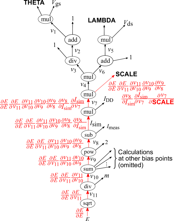
In the backward mode, the derivative of the output is propagated backwards through the graph to calculate the partial derivative with respect to each model parameter, as shown in Fig. 3, in which the path to calculate has been highlighted as an example. There are eight vertices (, , , , , , , and ) on the path. According to the chain rule, is calculated as follows:
| (5) |
The derivative of each edge with respect to the previous edge can be easily obtained: because . Similarly, as , and as . Substituting all the derivatives in (III-B) with the partial derivatives of the edges obtained by traversing the graph, the following equation is derived:
| (6) |
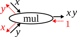
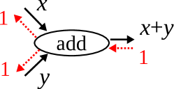
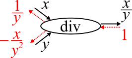
The values of , , and were already stored while progressing the forward mode. The partial derivatives are calculated for all model parameters and the resulting set of partial derivatives is used as a gradient in the parameter updating phase. The chain rule provides us with a way to easily and efficiently calculate the gradients without approximation. The edges of the graphs for forward and backward propagations can be determined by simply consulting the rules as summarized in Fig 4.
We would like to note that the partial derivative shown in (6) is the value of a single bias condition. When there are multiple bias conditions, which is usually the case, the backward propagation explained above is carried out for all bias conditions. That is, at the sum node, the partial difference of all the paths contributing is calculated for each bias condition until the model parameter node is reached. The partial derivatives of the model parameters are the summation of the partial derivatives of the different bias voltages diverged at the sum node.
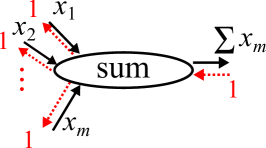

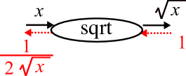
The computational graph must be constructed only once for a given MOSFET model. The construction can be very quick as described in the experimental section. Additionally, once the computational graph is generated, it can be reused as long as the same MOSFET model is used; therefore, the time needed to construct the computational graph is virtually negligible. Besides, since building a computational graph on the basis of model equations, either model equations or source code, at least, is required as a prerequisite for applying the proposed parameter extraction. Note that the extracted model parameters by the proposed method bears physical meaning when physics-based model is used as the computational graph is consistent with the model equations. Thus, the estimated model parameters can be used for device characterization, such as manufacturing variability analysis.
IV Experiments
To quantitatively evaluate the effectiveness of the proposed method, the model parameters for two different MOSFET models were extracted using AD- and ND-based parameter extraction. A commercially available silicon carbide (SiC) power MOSFET [22] was used for these measurements. The experiments were conducted using a Linux PC with an Intel Xeon W5590 3.33 GHz central processing unit (CPU) using a single thread. The extraction was implemented using the Python programming language.
IV-A MOSFET Models
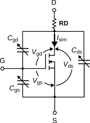
The two MOSFET models used in this section are an -th-power-law model [12] and a surface-potential-based model [6]. The equivalent circuit of SiC power MOSFET is shown in Fig. 5. The MOSFET model characterizes the current characteristics and three terminal capacitances: gate-source capacitance , drain-source capacitance , and gate-drain capacitance . The parameter extraction for the -the-power-law model uses only, while that for the surface-potential-based model uses , , and in this experiment. Note that is modeled as constant as in [6].
IV-A1 -th-Power-Law Model
In this model, the drain current is calculated based on the threshold voltage, , of the MOSFET. The saturation voltage, , and saturation current, , are defined as
| (7) | ||||
| (8) |
where and are the fitting parameters used to calculate the current in the linear region and and are other fitting parameters that are used for the saturation region. replaces to represent a smooth transition between the linear and saturation regions [6]:
| (9) |
where controls the smoothness of the transition between and . The drain current, , is calculated based on the channel length modulation and mobility degradation [23, 24] as follows:
| (10) |
The model parameters of the -th-power-law model are listed in Table I.
| Parameter | Description |
|---|---|
| VTH | Threshold voltage [V] |
| K | Fitting parameter for the linear region [-] |
| M | Fitting parameter for the linear region [-] |
| J | Fitting parameter for the saturation region [-] |
| N | Fitting parameter for the saturation region [-] |
| LAMBDA | Channel length modulation [1/V] |
| THETA | Mobility degradation [1/V] |
| DELTA | Smoothing parameter for gradual transition |
| between the linear and saturation regions [-] |
IV-A2 Surface-Potential-Based Model
| Model parameter | Description |
|---|---|
| TOX | Oxide thickness [m] |
| VFBC | Flat-band voltage of the channel region [V] |
| NA | Acceptor concentration [] |
| SCALE | Current gain factor [] |
| RD | Parasitic resistance at the drain side [] |
| LAMBDA | Channel length modulation [1/V] |
| THETA | Channel mobility degradation [1/V] |
| DELTA | Smoothing parameter for gradual transition |
| between the linear and saturation regions [-] |
| Model parameter | Description |
|---|---|
| ADS | Drain-source overlap area [] |
| ND | Donor concentration [] |
| VBI | Built-in potential of PN junction [V] |
| COXD | Gate-drain oxide capacitance [F] |
| AGD | Gate-drain overlap area [] |
| VFBD | Gate-drain flat-band voltage [V] |
| Parameter | Description | Value |
|---|---|---|
| Boltzmann’s constant [] | ||
| Elementary charge [C] | ||
| Absolute temperature [K] | 298 | |
| Thermal voltage () [V] | 0.026 | |
| Permittivity of SiC [F/m] | ||
| Permittivity of gate oxide [F/m] | ||
| Intrinsic carrier concentration | ||
| of SiC [] |
The proposed parameter extraction is also performed on the surface-potential-based model, which was developed to simulate the behavior of a SiC power MOSFET [6]. The model parameters of the current and capacitance model equations are listed in Tables II and III, respectively. The physical constants for these models are summarized in Table IV.
According to the current model in [6], the surface potentials, , and are first calculated for the source and drain ends of the channel as functions of and . The inverted charge of the channel is determined as a function of the surface potential. Then, the intermediate value in (4) is computed based on and as follows:
| (11) |
where
| (12) |
Here, and are the Boltzmann’s constant and the absolute temperature, respectively. is the permittivity of SiC, is the thermal voltage, and is gate oxide capacitance per unit area. Further, , where and TOX are the permittivity and thickness, respectively, of the gate oxide. VFBC and NA are the flat-band voltage and the acceptor concentration, respectively. The channel current model also includes a smooth transition between the linear and saturation regions according to the model parameter DELTA, which is defined by a similar equation to that in the -th-power-law model. Finally, substituting in (11), the simulated drain current, , is derived. The drain current in the structure also depends on the parasitic resistance RD [5] which reduces internal drain voltage of the MOSFET.
In the surface-potential-based model, the calculation of and involves solving a non-linear equation [1], whose solution cannot be explicitly expressed. Typically, the surface potentials have to be obtained using iterative methods [23, 5] such as the Newton-Raphson method. Though the computational graph may also be constructed for the model equations containing iterations, we adopt the following closed-form expression for the surface potential [25] for simplifying the calculation graph:
| (13) |
and are derived by solving (13) with respect to at and , respectively. Thus, the model equations of the surface-potential-based model can be entirely represented by a computational graph.
The capacitance characteristics, and , are expressed in the surface-potential-based model as follows:
| (14) | ||||
| (15) |
is a bias-dependent junction capacitance between drain and source, which is calculated on the basis of the capacitance model of the PN junction as shown in (14). is modeled as a series connection of the constant gate oxide capacitance and the bias-dependent depletion-layer MOS capacitance . Here, is a MOS capacitance represented as a function of the surface potential of the channel formed on the drain region under the junction field effect transistor (JFET) region. It can be written as shown in (16), where is computed in a similar way to the calculation of using (13) with (, , , ).
| (16) |
IV-A3 Initial Parameter Determination
The initial parameter determination is one of the important steps in the model development because the model parameters are repeatedly updated to minimize the discrepancy with the measured device characteristics, starting from the initial values. When the choice of the initial parameters is inappropriate, the model parameters may be determined as a local optimum solution that can be far from the ground truth. The standardized compact models provide the initial parameter determination as well as the model descriptions [26, 27]. In the experiment, we apply an initial parameter determination for the surface-potential-based model proposed in [28]. In this work, we assume TOX is 50 nm. The default value of DELTA, which is introduced to model the gradual transition between the linear and saturation regions, is set to 0.8 [27].
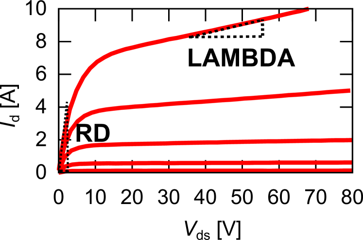
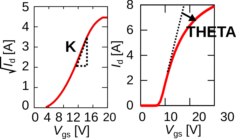
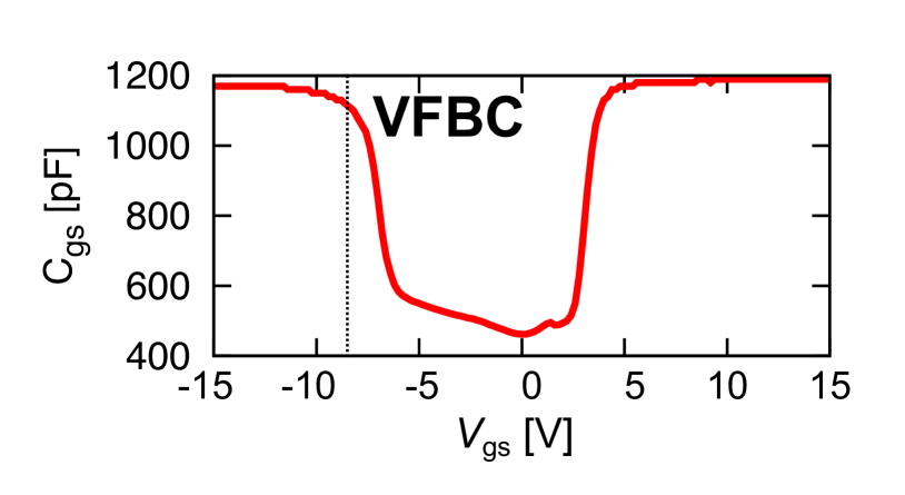
The slope of the - curve in the saturation region is represented by LAMBDA, while that at V of a high shows RD as shown in Fig. 9. K and THETA are extracted from the - curve as shown in Fig. 9. K is approximated by the slope of saturation-region current, and THETA is extracted from the linear region current. VFBC is the flat-band voltage of the MOS interface at the channel region. Beyond that voltage, the depletion capacitance becomes apparent in the MOS capacitance characteristics. Hence, VFBC can be estimated from the gate-source capacitance against at which starts to bend, as shown in Fig. 9.
As a good estimate, we approximate to a PN junction capacitance that depends on drain-source voltage [29]:
| (17) |
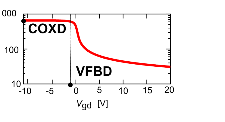
As shown in Fig. 9, VFBD and COXD are obtained as the capacitance in the accumulation mode. AGD is estimated as . Then, by substituting VFBD, COXD, and AGD to (17), ND can be calculated. Finally, NA is obtained from
| (18) |
where is the intrinsic carrier concentration. VBI is derived as the forward voltage where the body-diode current starts to flow. ADS is calculated by substituting VBI and ND to (14).
IV-A4 Computational Graph
The computational graphs of the two models were constructed based on the respective model equations. Graph manipulations are implemented using a Python package, NetworkX [30]. As shown in Table V, the execution time was much less than 0.1 second on the single thread PC for both models. Table VI summarizes the sizes of the two computational graphs from the input parameters to for a particular bias voltage. The subgraph for calculating is reused for different bias voltages. The graph size of the surface-potential-based model is approximately ten times larger than that of the -th-power-law model. Thus, only the computational graph of the -th-power-law model is presented in Fig. 10. Through defining the forward and backward functions of each node and incorporating the computational network into Algorihgm 3, the AD-based parameter extraction is carried out according to Algorithm 1.

| Model | Time [s] | |
|---|---|---|
| -th-power-law model | 0.0384 | |
| Surface-potential-based model | 0.0571 | |
| 0.0039 | ||
| 0.0288 | ||
| Model | No. of Edges | No. of Vertices | |
|---|---|---|---|
| -th-power-law model | 39 | 48 | |
| Surface-potential-based model | 384 | 540 | |
| 20 | 20 | ||
| 318 | 228 | ||
IV-B Simulation Setup
I-V curves of the SiC MOSFET [22] were measured at room temperature using a dedicated curve tracer [31] while sweeping from 6 V to 14 V with 2 V steps and sweeping from 0 V to 50 V with 2 V steps (the total number of bias voltages tested , were 125). C-V curves were measured by a commercial curve tracer [32] at 1 MHz. The data points are 300 for both and measurements. The parameter updating process was conducted by using AdaGrad [18]:
| (19) | |||||
| (20) |
The parameter update is performed to decrease the RMSE between the measured drain current and that obtained through the MOSFET model with the latest model parameters. In AdaGrad, the parameter vector, , is introduced. Based on the gradient, is gradually reduced as shown in (19) and (20). Generally, the initial values of all elements of were set to zero and all elements of were set to 1/100 for the respective parameter values.
IV-C Results
IV-C1 Parameter extraction for current characteristics
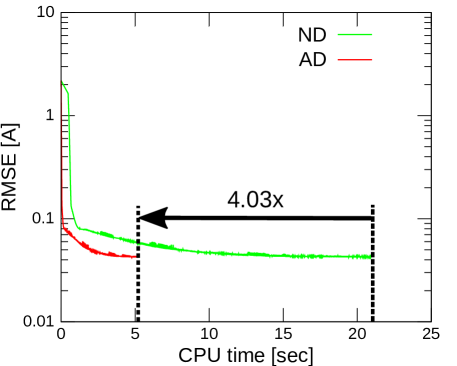
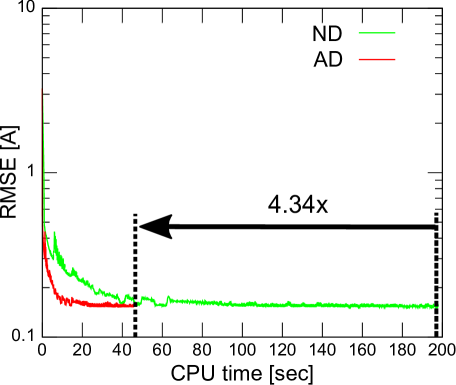
The parameters extracted by the proposed AD-based approach was compared with those by the ND-based method using each of the two MOSFET models. In this experiment, the maximum number of iterations, , was set to 1,000 for both the models. Also, was set to 0.04 A and 0.16 A for each model. The initial values are randomly determined for the -th-power-law model, while those of the surface-potential-model are determined by the initial parameter determination procedure described in Section IV-A3. Fig. 11 shows the RMSE as function of the computation time. The proposed method accelerated the parameter extraction by 4.03 and 4.34 for the -th-power-law model and the surface-potential-model, respectively. This improvement in the computation time was close to the theoretical value of 4.5 () for a generalized model with eight parameters.
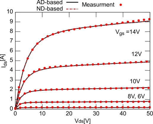
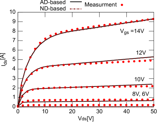
The measured and simulated I-V characteristics of the two models are presented in Fig. 12. The final model parameters extracted using the AD and ND methods are used to generate the graph. These results show that both MOSFET models accurately reproduced the I-V characteristics of the SiC MOSFET. The extracted parameter values at are summarized in Tables VII and VIII. Also, the initial values are listed in Table VIII for the surface-potential-based model. The relative error was smaller than 2% in all cases. In addition, it can be seen from Table VIII that the initial and the optimized parameters are close with each other, suggesting that the good initial parameters have been extracted through the procedure. Hence, it was concluded that the proposed method accelerates parameter extraction without affecting the accuracy.
| Relative | |||
| Parameter | AD | ND | error [%] |
| VTH | 2.600 | 2.600 | 0.116 |
| K | 0.372 | ||
| N | 3.284 | 3.286 | 0.061 |
| LAMBDA | 0.576 | ||
| THETA | 0.610 | ||
| M | 1.743 | 1.744 | 0.057 |
| J | 0.119 | 0.119 | 0.000 |
| DELTA | 1.269 | 1.267 | 0.158 |
| Parameter | Relative | ||
|---|---|---|---|
| (Initial value) | AD | ND | error [%] |
| SCALE | |||
| (5166360) | 5403054 | 5398779 | 0.079 |
| TOX | |||
| () | 0.035 | ||
| NA | |||
| () | 0.000 | ||
| LAMBDA | |||
| () | 0.387 | ||
| VFBC | |||
| () | 1.869 | ||
| THETA | |||
| () | 0.492 | ||
| DELTA | |||
| () | 0.6170 | 0.6150 | 0.329 |
| RD | |||
| () | 0.715 |
IV-C2 Parameter extraction for multiple objectives
The proposed method can handle model parameters used in different model equations. Since TOX and NA are contained in the current and capacitance characteristics, and , in the surface-potential-based model, these parameters have to be consistent for both characteristics. In this experiment, the computational graphs were constructed so that the parameters are simultaneously optimized for all the model equations. The cost function is set as the normalized sum of the residuals to balance the weights of each characteristic. The initial values of the parameters are determined through the determination procedure. In this experiment, was added as the termination condition, in addition to iteration count . Since VBI can be represented using NA and ND as shown in (18), the total number of the model parameters thus is 13 excluding VBI.
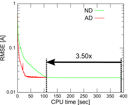
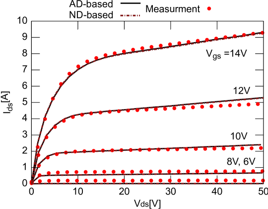
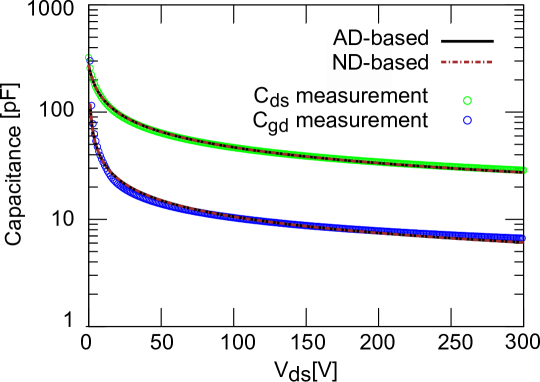
Fig. 13 shows the RMSE as function of computation time for the simultaneous parameter extraction. The proposed method calculates the model parameters 3.50 faster than the ND-based parameter extraction. The measured and simulated I-V and C-V characteristics of the models are presented in Fig. 14. The graphs are plotted by the final model parameters extracted using the AD and ND methods. Form the results, good agreement can be seen among the I-V and C-V characteristics. The initial and extracted parameter values when the algorithm exits are summarized in Table IX. The relative error between the parameters extracted by using the AD and ND methods was smaller than 3% in all the parameters. From the result, we confirmed that the proposed method is applicable for the capacitance characteristics, and the simultaneous parameter extraction of the different characteristics.
| Model parameter | Relative | ||
|---|---|---|---|
| (Initial value) | AD | ND | error [%] |
| SCALE | |||
| (5166360) | 5644684 | 5574780 | 1.238 |
| TOX | |||
| () | 0.286 | ||
| NA | |||
| () | 0.000 | ||
| LAMBDA | |||
| () | 0.589 | ||
| VFBC | |||
| () | 2.168 | ||
| THETA | |||
| () | 0.287 | ||
| DELTA | |||
| (0.80) | 0.6073 | 0.6130 | 0.938 |
| RD | |||
| () | 1.744 | ||
| ADS | |||
| (0.00776) | 0.0250 | 0.0250 | 0.000 |
| ND | |||
| () | 0.000 | ||
| COXD | |||
| () | 0.000 | ||
| VFBD | |||
| () | 0.1055 | 0.1055 | 0.000 |
| AGD | |||
| () | 0.000 |
IV-C3 Parameter extraction using LM method
In addition to the gradient-descent-based method, the proposed method can be applied to various optimization algorithms that rely on derivatives. Here, we show the result of the parameter extraction derived by incorporating the proposed method with the LM method, which is adopted in a widely used industrial device modeling flow [33].
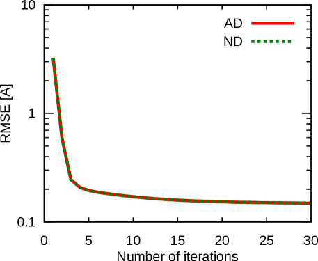
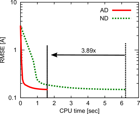
Fig. 15 shows the RMSE reduction in the LM-based parameter extraction. In this experiment, the model parameters of the surface-potential-based model are extracted by using the same initial parameters as those in Sec. IV-C1. Owing to the quadratic convergence property of the LM algorithm [34], the number of iterations is reduced to 30 for both the AD- and ND-based calculations, while the gradient-descent-based method requires more than six hundred iterations as shown in Fig. 15(a). As expected, close to the ideal 3.89 acceleration has been obtained, as shown in Fig. 15(b). In addition, the extracted parameters by the AD- and ND-based calculations, which are shown in Table X, are in perfect agreement, and quite close to those in Table VIII. From these results, the proposed method can be successfully applied to other derivative-based optimization algorithms, and the accelerations according to the number of parameters can be achieved.
| Parameter | Relative | ||
|---|---|---|---|
| (Initial value) | AD | ND | error [%] |
| SCALE | |||
| (5166360) | 516636 | 516636 | 0.000 |
| TOX | |||
| () | 0.000 | ||
| NA | |||
| () | 0.000 | ||
| LAMBDA | |||
| () | 0.000 | ||
| VFBC | |||
| () | 0.000 | ||
| THETA | |||
| () | 0.000 | ||
| DELTA | |||
| () | 0.614 | 0.614 | 0.000 |
| RD | |||
| () | 0.000 |
IV-D Manufacturing variability analysis
Recently, the application of artificial intelligence has been gaining popularity in the area of power electronics [35]. As an example, a neural network has been applied to model the device current characteristics in SPICE simulators [36] considering the parameter fitting as a black-box regression with a neural network. However, as opposed to the physics-based modeling, neural networks carry out purely mathematical fitting of the measured device characteristics to a nonlinear equation, ignoring physical behavior of the device in interest. In order to fully understand various device characteristics such as aging-induced threshold voltage shift [37] and manufacturing process variation [38, 39], which have been critical issues in the design of power converters using wide-bandgap semiconductors, the usage of a set of physically meaningful model parameters is of enormous importance. Although the proposed method incorporates a similar technique used in neural networks for model-parameter extraction, our method preserves the physical meanings of the model parameters.
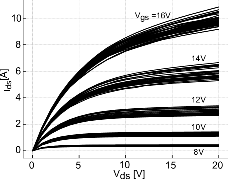
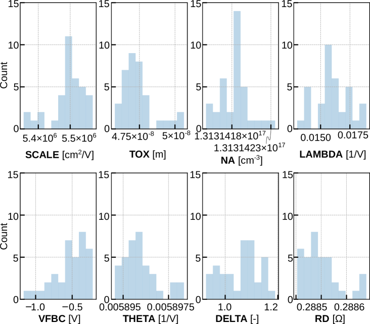
In order to demonstrate the aforementioned advantages, we apply the proposed method to the modeling of I-V characteristics of 35 SiC MOSFETs, which are presented in Fig. 16. For instance, in the parallel operation of SiC MOSFETs in a power module, the characteristics mismatch causes the current imbalances, resulting in the significant degradation of the reliability [38]. By applying the proposed method with the surface-potential-based model, the distribution of its model parameters can be obtained as shown in Fig. 17. We would like to note that the extracted model parameters represent their variation while the neural network based method [36] only gives us 35 black box models consisting of slightly different parameters. According to [39], the current imbalance can be mitigated by pairing MOSFETs with similar threshold voltage () and/or current gain factor () in parallelly connected SiC MOSFETs. Choosing pairs could be easy with the parameters obtained by the proposed method. Moreover, the distribution of the physically meaningful parameters, such as TOX and NA, can also be used by manufacturers to improve manufacturing yields.
V Conclusion
Herein, we proposed a novel parameter-extraction method that is applicable to various power MOSFET models. The proposed method employs AD, which is commonly used in backpropagation of artificial neural networks. The AD technique involves the calculation of the partial derivatives according to the chain rule by simply traversing the calculation graph, thereby reducing the number of times the model equation must be evaluated compared to ND calculation. Due to this improvement, the AD approach requires less computation time than the ND approach for parameter extraction. Experimental results using a commercial SiC power MOSFET demonstrated that the proposed method could be used to successfully derive the model parameters for the current equation of the MOSFET about 4.3 times faster than the conventional gradient-descent method using two-point gradient approximations.
In future study, we intend to include an evaluation with open source packages for AD as introduced in [40] to analyze more complex descriptions in arbitrary power MOSFET models by the computational graph. In addition, the evaluation of the proposed method is still limited in the static characteristics. We intend to investigate a further evaluation on the dynamic characteristics based on the extracted parameters.
Acknowledgment
This work was partially supported by JST-OPERA Program Grant Number JPMJOP1841, Japan. The part of this work is also supported by JSPS KAKENHI Grant 20H04156 and 20K21793.
Appendix
The proposed method can be applied even when the model contains loops, such as “while” or “for” statements. The computational graph of the loop is constructed with a feedback loop. In the forward mode, the computational graph is repeatedly traversed until the convergence condition is satisfied. Here, the variables of the graph are extended to use a stack data structure so that the intermediate values for each calculation are pushed into it. The backward mode is conducted by popping the variables while traversing the graph. Here, the while statement essentially contains a conditional branch. Meanwhile, some models also contain “if” statement, so that different calculations are carried out depending on the bias condition or the parameter. In the proposed method, the conditional branch is realized by adding a flag to the node again as a stack to judge which path should be selected. The backward mode is carried out by traversing the graph according to the flag value.
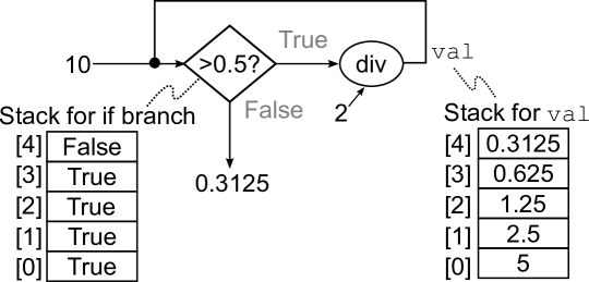
Fig. 18 shows a computational graph of a while statement in the following code snippet as an example.
In this code, variable val is initialized to 10, then changes to 5, 2.5, 1.25, 0.625, and 0.3125. Finally, the loop terminates when its value becomes smaller than 0.5. The computational graph of the while statement is constructed with a feedback loop containing a conditional branch and stacks as shown in Fig. 18. In the forward mode, the model equation is evaluated while pushing the value of variable val into the stack sequentially. In addition, the flags that will be used to which path should be evaluated are stored in the stack. Then, in the backward mode, the graph is traversed by popping these values.
References
- [1] B. Jayant Baliga, Fundamentals of Power Semiconductor Devices. Springer, 2008, p. 15.
- [2] T. Kimoto and J. A. Cooper, Fundamentals of Silicon Carbide Technology: Growth, Characterization, Devices and Applications. Wiley, 2014, p. 330.
- [3] Z. Liu, B. Li, F. C. Lee, and Q. Li, “High-efficiency high-density critical mode rectifier/inverter for WBG-device-based on-board charger,” IEEE Transactions on Industrial Electronics, vol. 64, no. 11, pp. 9114–9123, 2017.
- [4] K. Akatsu and S. Tanimoto, “Air-cooled multi-phase dual-winding in-wheel motor integrated with ultra small SiC module,” in Proceedings of IEEE Energy Conversion Congress and Exposition, 2020, pp. 41–46.
- [5] H. J. Mattausch, M. Miyake, T. Iizuka, H. Kikuchihara, and M. Miura-Mattausch, “The second-generation of HiSIM_HV compact models for high-voltage MOSFETs,” IEEE Transactions on Electron Devices, vol. 60, no. 2, pp. 653–661, 2013.
- [6] M. Shintani, Y. Nakamura, K. Oishi, M. Hiromoto, T. Hikihara, and T. Sato, “Surface-potential-based silicon carbide power MOSFET model for circuit simulation,” IEEE Transactions on Power Electronics, vol. 33, no. 12, pp. 10 774–10 783, 2018.
- [7] H. Agarwal, C. Gupta, R. Goel, P. Kushwah, Y.-K. Lin, M.-Y. Kao, J.-P. Duarte, H.-L. Chang, Y. S. Chauhan, S. Salahuddin, and C. Hu, “BSIM-HV: High-voltage MOSFET model including quasi-saturation and self-heating effect,” IEEE Transactions on Electron Devices, vol. 66, no. 10, pp. 4258–4263, 2019.
- [8] M. Albrecht, F. J. Klüpfel, and T. Erlbacher, “An iterative surface potential algorithm including interface traps for compact modeling of SiC-MOSFETs,” IEEE Transactions on Electron Devices, vol. 67, no. 3, pp. 855–862, 2020.
- [9] Y. Li and Y.-Y. Cho, “Intelligent BSIM4 model parameter extraction for sub-100 nm MOSFET era,” Japanese Journal of Applied Physics, vol. 43, no. 4B, pp. 1717–1722, 2004.
- [10] Q. Zhou, W. Yao, W. Wu, X. Li, Z. Zhu, and G. Gildenblat, “Parameter extraction for the PSP MOSFET model by the combination of genetic and Levenberg-Marquardt algorithms,” in Proceedings of International Conference on Microelectronic Test Structures, 2009, pp. 137–142.
- [11] M. Shintani, M. Hiromoto, and T. Sato, “Efficient parameter-extraction of SPICE compact model through automatic differentiation,” in Proceedings of International Conference on Microelectronic Test Structures, 2018, pp. 35–42.
- [12] T. Sakurai and A. R. Newton, “A simple MOSFET model for circuit analysis,” IEEE Transactions on Electron Devices, vol. 38, no. 4, pp. 887–894, 1991.
- [13] M. Bartholomew-Biggs, S. Brown, B. Christianson, and L. Dixon, “Automatic differentiation of algorithms,” Journal of Computational & Applied Mathematics, vol. 124, no. 1, pp. 171–190, 2000.
- [14] A. G. Baydin, B. A. Pearlmutter, A. A. Radul, and J. M. Siskind, “Automatic differentiation in machine learning: a survey,” Journal of Machine Learning Research, vol. 18, no. 153, pp. 1–43, 2018.
- [15] Y. LeCun, Y. Bengio, and G. Hinton, “Deep learning,” Nature, vol. 521, 2015.
- [16] D. W. Marquardt, “An algorithm for least-squares estimation of nonlinear parameters,” Journal of the Society for Industrial and Applied Mathematics, vol. 11, no. 2, pp. 431–441, 1963.
- [17] K. Takeuchi and M. Hane, “Statistical compact model parameter extraction by direct fitting to variations,” IEEE Transactions on Electron Devices, vol. 55, no. 6, pp. 1487–1493, 2008.
- [18] J. Duchi, E. Hazan, and Y. Singer, “Adaptive subgradient methods for online learning and stochastic optimization,” Journal of Machine Learning Research, vol. 12, pp. 2121–2159, 2011.
- [19] M. D. Zeiler, “AdaDelta: An adaptive learning rate method,” 2012. [Online]. Available: https://arxiv.org/abs/1212.5701
- [20] J. Schulman, N. Heess, T. Weber, and P. Abbeel, “Gradient estimation using stochastic computation graphs,” in Proceedings of Neural Information Processing Systems Conference, 2015, pp. 3528–3536.
- [21] A. Griewank, “Achieving logarithmic growth of temporal and spatial complexity in reverse automatic differentiation,” Optimization Methods and Software, vol. 1, pp. 35–54, 1992.
- [22] ROHM Co., Ltd., SCT2450KE N-channel SiC power MOSFET Datasheet, 2013.
- [23] M. Miura-Mattausch, N. Sadachika, D. Navarro, G. Suzuki, Y. Takeda, M. Miyake, T. Warabino, Y. Mizukane, R. Inagaki, T. Ezaki, H. J. Mattausch, T. Ohguro, T. Iizuka, M. Taguchi, S. Kumashiro, and S. Miyamoto, “HiSIM2: Advanced MOSFET model valid for RF circuit simulation,” IEEE Transactions on Electron Devices, vol. 53, no. 9, pp. 1994–2007, 2006.
- [24] G. Gildenblat, X. Li, W. Wu, H. Wang, A. Jha, R. van Langevelde, G. D. J. Smit, A. J. Scholten, and D. B. M. Klaassen, “PSP: An advanced surface-potential-based MOSFET model for circuit simulation,” IEEE Transactions on Electron Devices, vol. 53, no. 9, pp. 1979–1993, 2006.
- [25] T. L. Chen and G. Gildenblat, “Analytical approximation for the MOSFET surface potential,” Solid-State Electronics, vol. 45, no. 2, pp. 335–339, 2001.
- [26] “BSIM4v4.8.0 MOSFET Model User’s Manual,” https://bsim.berkeley.edu/models/bsim4/, [Online available].
- [27] “HiSIM_HV 2.2.0 User’s Manual,” http://home.hiroshima-u.ac.jp/usdl/HiSIM_HV/index.html, [Online available].
- [28] M. Shintani, H. Tsukamoto, and T. Sato, “Parameter extraction procedure for surface-potential-based SiC MOSFET model,” in Proceedings of IEEE Workshop on Wide Bandgap Power Devices and Applications, 2019, pp. 444–448.
- [29] N. Phankong, T. Yanagi, and T. Hikihara, “Evaluation of inherent elements in a SiC power MOSFET by its equivalent circuit,” in Proceedings of European Conference on Power Electronics and Applications, 2011, pp. 1–8.
- [30] A. A. Hagberg, D. A. Schult, and P. J. Swart, “Exploring network structure, dynamics, and function using NetworkX,” in Proceedings of Python in Science Conference, 2008, pp. 11–15.
- [31] Y. Nakamura, M. Shintani, T. Sato, and T. Hikihara, “A high power curve tracer for characterizing full operational range of SiC power transistors,” in Proceedings of International Conference on Microelectronic Test Structures, 2016, pp. 90–94.
- [32] Keysight Technologies, Inc., B1505A Power Device Analyzer/Curve Tracer, 2014.
- [33] ——, IC-CAP Device Modeling Software, 2014.
- [34] J.-Y. Fan and Y.-X. Yuan, “On the quadratic convergence of the Levenberg-Marquardt method without nonsingularity assumption,” Computing, vol. 74, pp. 23–39, 2005.
- [35] S. Zhao and H. Wang, “An overview of artificial intelligence applications for power electronics,” IEEE Transactions on Power Electronics, vol. 36, no. 4, pp. 4633–4658, 2021.
- [36] D. Chiozzi, M. Bernardoni, N. Delmonte, and P. Cova, “A neural network based approach to simulate electrothermal device interaction in SPICE environment,” IEEE Transactions on Power Electronics, vol. 34, no. 5, pp. 4703–4710, 2019.
- [37] G. Rescher, G. Pobegen, T. Aichinger, and T. Grasser, “Preconditioned BTI on 4H-SiC: Proposal for a nearly delay time-independent measurement technique,” IEEE Transactions on Electron Devices, vol. 65, no. 4, pp. 1419–1426, 2018.
- [38] G. Wang, J. Mookken, J. Rice, and M. Schupbach, “Dynamic and static behavior of packaged silicon carbide MOSFETs in paralleled applications,” in Proceedings of IEEE Applied Power Electronics Conference, 2014, pp. 1478–1483.
- [39] A. Borghese, M. Riccio, A. Fayyaz, A. Castellazz, L. Mares, G. Bregl, and A. Irace, “Statistical analysis of the electrothermal imbalances of mismatched parallel SiC power MOSFETs,” IEEE Journal of Emerging and Selected Topics in Power Electronics, vol. 7, no. 3, pp. 1527–1538, 2019.
- [40] Community Portal for Automatic Differentiation, [Online Available]. http://www.autodiff.org.