Intrinsic RESET speed limit of valence change memories
Abstract
During the last decade, valence change memory (VCM) has been extensively studied due to its promising features, such as a high endurance and fast switching times. The information is stored in a high resistive state (logcial ‘0’, HRS) and a low resistive state (logcial ‘1’, LRS). It can also be operated in two different writing schemes, namely a unipolar switching mode (LRS and HRS are written at the same voltage polarity) and a bipolar switching mode (LRS and HRS are written at opposite voltage polarities). VCM, however, still suffers from a large variability during writing operations and also faults occur, which are not yet fully understood and, therefore, require a better understanding of the underlying fault mechanisms. In this study, a new intrinsic failure mechanism is identified, which prohibits RESET times (transition from LRS to HRS) faster than 400 ps and possibly also limits the endurance. We demonstrate this RESET speed limitation by measuring the RESET kinetics of two valence change memory devices (namely Pt/TaOx/Ta and Pt/ZrOx/Ta) in the time regime from 50 ns to 50 ps, corresponding to the fastest writing time reported for VCM. Faster RESET times were achieved by increasing the applied pulse voltage. Above a voltage threshold it was, however, no longer possible to reset both types of devices. Instead a unipolar SET (transition from HRS to LRS) event occurred, preventing faster RESET times. The occurrence of the unipolar SET is attributed to an oxygen exchange at the interface to the Pt electrode, which can be suppressed by introducing an oxygen blocking layer at this interface, which also allowed for 50 ps fast RESET times.
1 Introduction
Among other emerging memory technologies, valence change memory (VCM) can not only be used as binary storage class memory, but also to perform in-memory calculations or to realize neuromorphic applications [1, 2, 3, 4]. In the binary mode, the information is encoded in a high and a low resistive state (HRS and LRS). These two states can be programmed with electrical stimuli. The transition from the HRS to LRS is referred to as SET and the opposite transition as RESET. A VCM device usually consists of a mixed electronic-ionic conducting layer (e.g. TaOx or ZrOx), sandwiched between two asymmetric metallic electrodes [5, 6, 7, 8]. One of the two electrodes is inert (e.g. Pt) and referred to as active electrode, whereas the opposite electrode is oxygen affine (e.g. Ta). The devices are programmed by applying electrical stimuli, during which an n-conducting filament consisting of mobile donors is either formed (SET) or ruptured (RESET). Spectroscopic studies have identified these mobile donors as oxygen vacancies [9, 10, 11, 12, 13]. Especially for TaOx-based devices also a movement of metallic cations was observed [14, 15, 16]. During the SET, a negative voltage is applied to the active electrode (attracting mobile donors) and a positive voltage during the RESET (repelling mobile donors). As the voltages required for the SET and RESET have opposite signs, this corresponds to a bipolar switching mode.
For the binary switching mode, a high endurance of up to 1012 cycles [17, 18] and writing times below 1 ns[19, 20, 21, 22, 23, 24] have been reported. A successful market launch also requires high storage densities and, consequently, the integration of VCM devices into 3D structures [25]. Due to the presence of Joule heating during the SET [26, 27] and during the RESET operation [28], the writing time depends strongly non-linearly on the applied voltage[29, 30]. This non-linearity allows VCM devices to overcome the voltage-time-dilemma[31], which describes the necessity for high data retention during the read-out (at low voltages) and fast writing times (at high voltages) [32]. Programming VCM devices with shorter electrical stimuli also enhances the devices’ endurance [33, 34]. Calculations and simulations show that for nanoscale devices faster writing times of 1 ps are possible [35]. Sub-nanosecond switching times are still realizable, if the VCM devices were integrated into nanoscale crossbar array structures [36]. Also, first neuromorphic applications have been demonstrated on a sub-nanosecond timescale: Ma et al. recently demonstrated spike timing-dependent plasticity (STDP) in memristive devices with 600 ps pulses [37]. Concepts of GHz deep neural networks were developed, which are potentially faster than today’s CPUs and GPUs by a factor of 30,000 [38]. Most applications in the GHz regime require, consequently, fast writing times. So far, the speed limit was always attributed to the electrical charging of the devices, assuming that the intrinsic speed limit is only limited by the attempt frequency of the mobile donors in the THz domain [35].
Recently, we have shown that 50 ps fast SET times can be achieved for TaOx- and ZrOx-based VCM devices [39], which corresponds to the limitation of the experimental setup. We also demonstrated that the SET kinetics are mainly delayed by the electrical charging time in the sub-nanosecond regime and not by intrinsic processes, such as the migration of ions or the heating of the filamentary region [40]. The fast heating results from the narrow filament, which has only a diameter in the range from 1 nm to 3 nm [41]. While the SET kinetics have been studied quite extensively, studies investigating possible intrinsic RESET speed limits are rare. Most studies show only 10 or fewer successful RESET operations [21, 19, 20] and are not discussing possible RESET speed limitations. Only Wang et al. studied RESET kinetics in dependence on the applied voltage in the sub-nanosecond regime and observed a lower change in resistance at shorter pulse widths than 800 ps [22]. At pulse widths below 200 ps the VCM device switched randomly between the HRS and LRS. They explain this observation with a lower heating of the filamentary region during the RESET at shorter pulse widths than 800 ps. Their argumentation, however, does not account for the random switching between the LRS and the HRS.
In this study, we propose a different failure mechanism limiting the RESET kinetics in the sub-nanosecond regime: For this purpose, we focus on the RESET kinetics in the regime from 50 ns to 50 ps and show that they are intrinsically limited by the presence of a unipolar switching mode [42, 43]. Different to previous studies, we also acquired a much larger dataset to demonstrate the reproducibility of successful RESET operations. At slower timescales (above 700 ps) the RESET kinetics depend exponentially on the applied voltage, which was already demonstrated in other studies [28, 44, 45, 46, 47]. By increasing the applied voltage we could successfully reset the TaOx-based device within 670 ps at a voltage of 1.6 V and the ZrOx-based device within 480 ps at an voltage of 1.8 V. At higher voltages, the devices could not be driven to the HRS. Instead of an increase in resistance, a unipolar SET could be observed, decreasing the device’s resistance and, thereby, preventing faster RESET times.
This unipolar switching mode has already been observed for TaOx- [48] and ZrOx-based devices [49], but has never been considered as failure meachanism for neither the RESET kinetics, nor the endurance. It can be triggered by applying a positive voltage to the active electrode, with a higher amplitude compared to the RESET. This could result in a higher heating of the filamentary region than during the bipolar SET and RESET, which in turn could initiate thermo-diffusion of the mobile donors (also referred to as thermophoresis) [50]. To protect the device from damage, a current compliance is crucial during the unipolar SET, which also exhibits abrupt threshold switching. This switching mode was strongly investigated in the years up to 2013 in the hope of achieving a similar performance as for the bipolar switching mode. However, the current compliance to achieve the unipolar SET, has to be in the range of 1 mA [51], which increases the power consumption and the devices’ degradation during cycling. To our knowledge, the highest measured endurance of a unipolar switching mode amounts to only 106 cycles [52], being far worse than the endurance of the bipolar switching mode (1012 cycles [17]). As this mode prohibits faster RESET times and only achieves a poor performance with regard to power consumption and endurance, and also limits the writing time, it constitutes a failure mechanism.
The kinetics of this unipolar SET are also investigated in the time regime from 250 ps to 50 ps. We demonstrate that this unipolar SET event can be conducted within 50 ps. From the RESET and unipolar SET kinetics, we derive voltage programming windows, from which the intrinsic RESET speed limitation can be derived. Finally, we suppressed the oxygen exchange at the Pt electrodes with a 1.0 nm thin Al2O3 layer, which also allowed for 50 ps fast RESET times for both devices, which is - to our knowledge - the fastest reported RESET time of redox based random access memories (ReRAMs).
2 RESET kinetics
The RESET and unipolar SET kinetics measurements were conducted on a Pt/TaOx/Ta and a Pt/ZrOx/Ta device. Both devices have a size of µm2 and were also used in [39], showing that the SET operation can occur within 50 ps. The 30 nm thick Pt bottom electrode serves as active electrode. The film thickness of the TaOx and the ZrOx amounts to 5 nm and the film thickness of the Ta top electrode to 20 nm. Further information are given in the methods section. In recent publications, we have shown that devices with these material stacks have an endurance of at least 106 cycles [53, 54].
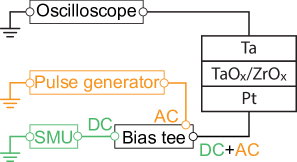

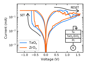
The experimental setup is sketched in Fig. 1(a) and is explained in detail in [39]. A pulse generator is connected to the alternating current (AC) port and a source measure unit (SMU) to the direct current (DC) port of a broadband bias tee. The combined DC + AC port of the bias tee is connected to the Pt bottom electrode of the VCM device, to which all indicated voltages in this paper were applied. Finally, the current response is measured with a real-time oscilloscope at the Ta top electrode. More information on the experimental setup is given in the methods section. The I(V)-characteristics of both devices are shown in Fig. 1(c).
To achieve proper impedance matching, both devices were integrated into coplanar waveguide (CPW) structures, consisting of three parallel stripes (ground-signal-ground, GSG). These CPW structures have gained more attention in recent years, as they can be used to realize radio frequency (RF) switches with memristive devices [55, 56]. Recently, we have shown for the TaOx-based device that the electrical charging occurs within less than 80 ps, if the device is integrated in a proper CPW structure [40]. The scattering parameters of both devices are shown in the supplementary Fig. S1. For these scattering parameters the devices’ charging times were derived in the supplementary Fig. S2, showing that the ZrOx-based device can even be charged within less than 70 ps.
The measurement procedure to determine the RESET kinetics on the timescale from 50 ns to 400 ps is depicted in Fig. 1(b). At the beginning of every cycle, the devices were driven to the LRS (ranging from 1.0 k to 3.0 k) by using a voltage sweep with an amplitude of -1.2 V at a sweep rate of 0.5 V/s. To protect the devices from damage a current compliance of 100 µA was used. The devices’ resistance was measured at a voltage of -0.2 V before and after the application of the pulse and is referred to as and , respectively. The RESET pulses’ amplitudes were adjusted between 1.2 V and 1.6 V111This is the effective pulse voltage seen by the device. The pulses emitted by the pulse generator only have half the amplitude. As the 50 transmission line is terminated with a high ohmic VCM device (even the resistance of the LRS is much larger than 50 ), the voltage at the device effectively doubles. This is due to the overlap of incoming pulse and the reflected pulse at the VCM device (see also supplementary section S.1 or [40]). At the end of each cycle, the device was driven to the HRS by applying a voltage sweep with an amplitude of 1.6 V at a sweep rate of 0.5 V/s. The pulse width was reduced with every increase in amplitude to reduce the stress on the device.
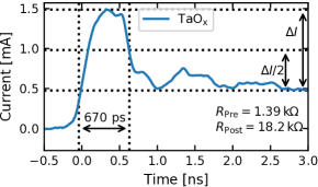
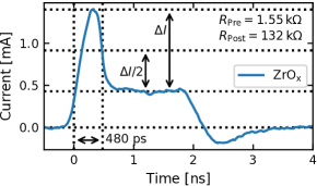
Two exemplary current responses to the applied voltage pulse are shown Fig. 2(a) and (b) for the TaOx and ZrOx-based device, respectively. In both cases, the current increases rapidly at the beginning of the pulse and decreases, subsequently, to values between 400 µA to 500 µA, which corresponds to the RESET. The contribution of the capacitive current is negligible. This can be seen at the end of the pulse applied to the ZrOx-based device in Fig. 2(b). The negative current peak corresponds to the capacitive current and is much smaller than the current peak at the beginning of the pulse. The RESET time is defined as the time difference between the time at which the current surpasses 20 % of the maximum current at the beginning of the pulse (first vertical dotted line in Fig. 2(a) and (b)) and the time at which the current reaches its half value (second vertical dotted line). The half value of the current /2 is defined as half the current difference between the minimum and the maximum current (see illustrations in Fig. 2(a) and (b)). A similar definition was used in our previous publications [28, 45].
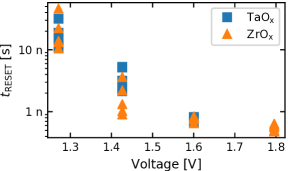
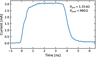
In case of the current response of the TaOx-based device in Fig. 2(a), a 10 ns pulse with an amplitude of 1.6 V was applied. During this pulse the device’s resistance increased from 1.39 k to 18.2 k and a RESET time of 670 ps was determined. By using higher pulse amplitudes, faster RESET times could be possible. Increasing the pulse amplitude to 1.8 V, however, resulted in dielectric breakdown and the device’s resistance started to decrease. This is shown in the supplementary Fig. S3. All determined RESET times are shown in Fig. 2(c) in dependence of the applied voltage. Up to a voltage of 1.6 V, the RESET time depends strongly non-linearly on the applied voltage, which was expected. At a voltage of 1.8 V (only values for ZrOx) the kinetics start to bend towards slower RESET times, which is attributed to the influence of the pulse generator’s rise time ( 360 ps).
To decrease the influence of the pulse generator’s rise time, the RESET kinetic measurements in the range from 250 ps to 50 ps were conducted with a faster pulse generator, having a rise time of only 35 ps. The measurement cycle is sketched in Fig. 3(a), and is almost identical to the previous (Fig. 1(b)), only the applied RESET pulse has changed. The pulse amplitude was once chosen to 1.6 V and once to 2.2 V. As in [39], the pulse width was increased from 50 ps to 250 ps in steps of 5 ps. Each cycle was repeated 10 times222The measurement cycles of the ZrOx-based device at a voltage of 1.6 V were repeated 20 times to achieve a smooth line of /..

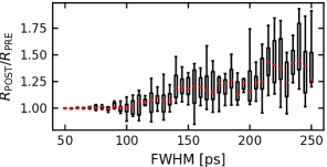
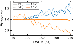
An exemplary measurement on the TaOx-based device at a voltage of 1.6 V is shown in Fig. 3(b). The ratio of the resistance before and after the pulse’s application is plotted as boxplot against the FWHM of the applied pulse. The red bar marks the median. As expected, the ratio / increases with increasing FWHM. The median of /, however, remains below 1.5 for all FWHMs, which means that no successful RESET occurs in this time interval333For a successful RESET operation the ratio of / should be greater than 3 [54]. The median values of / of all four measurements are shown in Fig. 3(c). The corresponding boxplots can be found in the supplementary Fig. S4. As the ratio / does not yield any information about the absolute resistance values, the values are shown in the supplementary Fig. S5. The initial resistances were always in the range from 1.0 k to 2.5 k.
At 1.6 V, the ratio / of the ZrOx-based device (dashed blue line in Fig. 3(c)) also remains below 2.0 for all FWHMs, indicating that the ZrOx-based device cannot be driven to HRS within 250 ps. At an amplitude of 2.2 V, / of the TaOx-based device (solid orange line in Fig. 3(c)) remained near unity for all FWHMs, while / of the ZrOx-based device (dotted orange line in Fig. 3(c)) decreased with increasing FWHM. Consequently, it is not possible with both devices to achieve RESET times faster than 250 ps by increasing the pulse amplitude. The decrease in resistance of the ZrOx-based device at 2.2 V indicates the presence of a unipolar switching mode.
3 Unipolar SET kinetics
The measurement procedure to determine the unipolar SET kinetics is depicted in Fig. 4(a). Different to the measurement procedures of the RESET kinetics, the device is driven to the HRS at the beginning of the measurement cycle by applying a voltage sweep with an amplitude of 1.6 V. The resulting resistance values were again in the range from 10 k to 30 k. At the end, it is driven to the LRS with a voltage sweep of -1.2 V. The sweep rate (0.5 V/s) and the current compliance during the SET sweep (300 µA) are identical to the values chosen in the RESET kinetics. The pulse amplitude was again varied from 50 ps to 250 ps and the amplitude from 1.6 V to 5.0 V. As the unipolar switching mode has a large variabilty for TaOx- [57] and ZrOx-based devices [58, 49], this cycle was repeated at least 10 times444The exact numbers are listed in Table S1 of the supplementary information., until smooth curves were achieved for /.

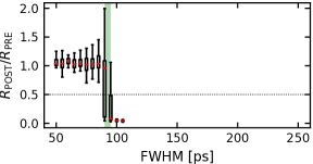
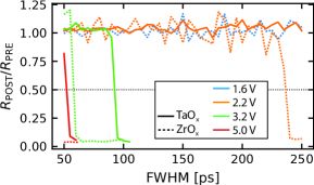
An exemplary measurements is shown in Fig. 4(b), in which voltage pulses with an amplitude of 3.2 V were applied to the TaOx-based device. A short FWHMs, the ratio / remains near unity, indicating that the resistance of the device does not change during the pulse’s application. At FWHMs of about 95 ps, / drops towards zero, indicating that the device was successfully driven to the LRS by applying a positive voltage pulse to the active Pt electrode. As the device is also driven to the HRS with a positive voltage pulse, this corresponds to a unipolar SET. At longer FWHMs, the measurement was aborted to prevent the device from damage.
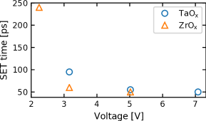
This measurement procedure was repeated at different amplitudes (from 1.6 V to 5.0 V) for the TaOx- and ZrOx-based devices. The median values are plotted in Fig. 4(c). The boxplot representation of / and the absolute values of are shown in the supplement Fig. S6-S9. Similar to our previous study, we defined the unipolar SET time, as the time, at which / reaches a value below 0.5 [39]. This threshold is indicated as horizontal dashed line in Fig. 4(c).
The resulting unipolar SET times are shown in Fig. 4(d) in dependence of the pulse voltage. The unipolar SET kinetics have similar fast switching times compared to the bipolar SET kinetics from [39]. Only the voltage has been shifted to higher absolute values. The fastest unipolar SET time amounts to 50 ps, which is - to our knowledge - the fastest unipolar SET measured in ReRAM devices. The fastest reported unipolar SET time, so far, amounts to 16 ns [59]. As the TaOx-based device did not switch at a pulse width of 50 ps an amplitude of 5.0 V to the LRS, a single measurement cycle with a pulse width of 50 ps and an amplitude of 7.1 V was repeated, during which the TaOx-based device switched to the LRS. Exemplary measured current transients, during which a unipolar SET time of 50 ps was realized, are shown in Fig. S10 of the supplementary information for both devices. The endurance of the unipolar switching mode was also tested. The TaOx and the ZrOx-based device reached an endurance of 104 cycles and 3590 cycles, respectively. The description of the measurement procedure and the results are shown in the supplementary Fig. S11. Usually, current compliances are required to realize unipolar switching modes [51]. In this study, the FWHM of the electrical stimuli is much shorter than state-of-the-art current compliances (often operating at time-scales above 1 µs[60]) and, therefore, the unipolar switching mode can be realized without current compliance.
4 Intrinsic RESET speed limitation
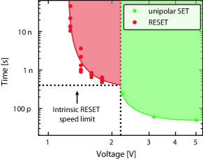
Although fast switching times are usually considered as promising feature, our interpretation of the fast unipolar SET time is that it should be considered as failure mechanism. At higher voltage amplitudes, the unipolar SET occurs faster than the RESET and, thereby, prohibits fast bipolar switching in both directions. This RESET speed limitation is illustrated in the following with RESET programming windows. These windows were estimated with the results from the RESET and the unipolar SET kinetics. As mentioned in the introduction, the unipolar switching mode observed in ReRAM devices, has less promising attributes with regards to endurance and switching power compared to the bipolar switching mode.
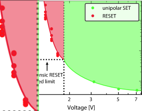
The results from the RESET kinetics (Fig. 2(c)) and the results from the unipolar SET kinetics (Fig. 4(d)) are plotted in Fig. 5. The red points mark the measured RESET times and the green points the measured unipolar SET times. The red and green shaded areas mark the voltage-time combinations at which either a RESET or a unipolar SET event is triggered. The green and red lines, encircling the red and green shaded area, are drawn by the eye. Their intersection is an estimate of the fastest possible RESET time, demonstrating that the presence of the unipolar switching mode intrinsically limits faster RESET times. In case of the TaOx-based device, this intersection occurs at 510 ps and in case of the ZrOx-based device at 400 ps, which marks their intrinsic RESET speed limit. It has, however, to be noted that this RESET programming window will vary from device to device and possibly also from cycle to cycle due to the high variability of the unipolar SET. This might also be the origin of the random switching between the HRS and the LRS in the results of Wang et al. [22]. In the sub-100 ps regime the measured unipolar SET events are also influenced by the electrical charging of the devices. At slower timescales, the unipolar SET is assumed to be time-independent.
5 Discussion
From Fig. 5, two possibilities to achieve faster RESET times can be derived:
-
1.
Lowering the RESET voltage
-
2.
Suppressing the unipolar switching mode
Torrezan et al. achieved 120 ps fast RESET times with a TaOx-based device [21]. The I(V) characteristics of their devices show that the RESET sets in at about 0.35 V [61]. In contrast, the RESET of the devices used in this study sets in above 0.5 V (see Fig. 1(c)). The device stack of both devices is very similar ([21]: Pt(20 nm)/TaOx(7 nm)/Ta(30 nm), this work: Pt(30 nm)/TaOx(5 nm)/Ta(20 nm). We therefore, assume that different fabrication processes are responsible for the lower RESET voltage.
Suppressing the unipolar SET or mitigating its impact on the bipolar RESET kinetics requires a better understanding of the underlying physical processes. The abrupt nature of the unipolar SET results from a thermal runaway (similar to the bipolar SET) [42]. This thermal runaway, however, does not necessarily lead to a permanent change in resistance. Especially TaOx also exhibits threshold switching [62]. The sudden current increase, may initiate an oxygen exchange between the oxide and the active Pt electrode, which leads to a permanent change in the device’s resistance. Such an exchange was also observed in the so-called “eightwise” switching mode, which has been observed in many transition metal oxides [63, 64, 65, 66], including TaOx-based devices [46]. This oxygen exchange could also be the origin of the permanent decrease in resistance during the unipolar SET, and could be suppressed in other studies by introducing an oxygen blocking layer such as C [46] or Al2O3 [64, 66].
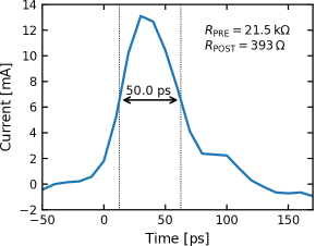
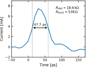
To test if an oxygen exchange also occurs during the unipolar SET between the oxide and the active Pt electrode, we introduced a 1.0 nm thick Al2O3 layer between the active Pt electrodes and the oxides, resulting in a Pt(30 nm)/Al2O3(1.0 nm)/TaOx(5 nm)/Ta(20 nm) and a Pt(30 nm)/Al2O3(1.0 nm)/ZrOx(5 nm)/Ta(20 nm) stack (referred to as Al2O3/TaOx and Al2O3/ZrOx device, respectively). We tested to reset both devices with 50 ps pulses. The measurement cycle is similar to the one from Fig. 3(a), only that this time the pulse width was fixed at 50 ps and the pulse amplitude was chosen to 5.0 V and 4.0 V for the Al2O3/TaOx and the Al2O3/ZrOx device, respectively. This measurement cycle was repeated 100 times for each device.
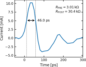
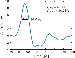
The results for and of the Al2O3/TaOx and the Al2O3/ZrOx device are shown in Fig. 6(a) and (b), respectively. During most cycles the devices switched to a higher resistance value after the application, showing that the additional Al2O3 layer improves the feasibility of fast RESET operations. As shown in Fig. 4(c) the devices without additional Al2O3 already started to switch to the LRS at a pulse amplitude of 5.0 V (red lines). To our knowledge, this is the first time that a 50 ps fast RESET process has been demonstrated for a ReRAM device. Two exemplary current responses are shown in Fig. 6(c) and (d) for the Al2O3/TaOx and Al2O3/ZrOx device, respectively. The FHWM of 50 ps has been preserved in both cases.
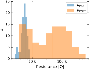
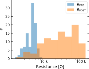
The devices did, however, also remain in the LRS sometimes, indicating that the 1.0 nm thick Al2O3 layer might only partially prohibit the oxygen exchange at the Pt active electrode and the remaining oxygen exchange might prohibit successful RESET operations. A similar observation was made by Zhang et al., who have placed an Al2O3 layer at the active electrode of a TiOx-based device to suppress the oxygen exchange at the active interface [64]. Their approach, however, only worked for Al2O3 layers thicker than 2 nm. Further studies with different oxygen blocking layers or different active electrodes are, consequently, necessary to achieve better control over the RESET process at these fast timescales.
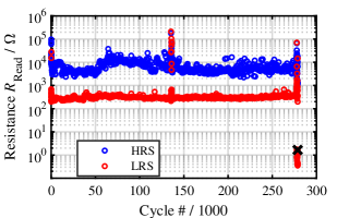
Another aspect of the unipolar SET is that it might limit the endurance of VCM based devices. During endurance measurements on ZrOx and TaOx-based devices, with very similar device fabrication, we observed that the devices were usually trapped in the LRS [67, 54], which might have been triggered by a unipolar SET event. An exemplary endurance measurement from [54], during which a ZrOx-based device got trapped in the LRS is shown in Fig. 7. In [67] the endurance limitation of TaOx-based devices was referred to as “RESET Failure”, which is characterized by an abrupt current increase during a RESET sweep. Afterwards, the devices were stuck in the LRS. This abrupt current increase is also observed during the unipolar SET, only that it is usually controlled with a current compliance [51].
6 Conclusion
In this study, we have demonstrated that the RESET kinetics of VCM-based devices are intrinsically limited by the coexistance of a unipolar switching mode. Therefore, the RESET kinetics of a TaOx and a ZrOx-based device were investigated in the regime from 50 ns to 50 ps. RESET times down to 480 ps could be achieved by increasing the voltage amplitude of the RESET pulse. At higher amplitudes, a unipolar SET event was triggered which prohibits faster RESET times and rather decreases the devices’ resistances. The unipolar SET kinetics were subsequently measured, showing that the unipolar SET can occur within 50 ps. We attribute the unipolar SET event to a thermal runaway, which followed by an oxygen exchange between the oxide and the active Pt electrode. This oxygen exchange could be partially suppressed by introducing a 1.0 nm thick Al2O3 layer between the oxide and the active electrode. With these devices 50 ps fast RESET operations could be repeated, but only stochastically. We also show, with the data from previous publications, that the occurrence of the unipolar SET limits the endurance of both devices. As the unipolar switching mode has less promising attributes than the bipolar switching mode, the unipolar SET needs to be treated as failure mechanism and further strategies should be developed to suppress its occurrence.
Methods
Device fabrication and structure: As substrate served a Si-wafer ( kcm). The top of the wafer was oxidized resulting in a 430 nm thick SiO2 layer. All deposition steps were conducted by means of RF magnetron sputtering. The µm2 devices were structured with optical lithography. More details on the device fabrication can be found in [68] and [69] for the TaOx- and the ZrOx-based device, respectively. The 1.0 nm Al2O3 layer was grown by atomic layer deposition (ALD), using trimethylaluminum (TMA) and a remote RF oxygen plasma source [64, 66]. This process ensures a uniform and dense Al2O3 layer on the sample surface.
The devices were formed with a voltage sweep with an amplitude of -4.0 V at a sweep rate of 0.5 V/s, applied to the active Pt electrode. A current compliance of 100 µA was used during the forming.
Both devices were integrated into a coplanar waveguide structure, having a length of 590 µm. The center signal stripe has a width of 100 µm and a spacing of 60 µm to the outer grounded stripes. At the center the inner conductor is tapered to 2 µm, matching the dimensions of the µm2 devices. More information and illustrations of this structures are given in [40].
Electrical characterization: The experimental setup is sketched in Fig. 1. The voltage sweeps and read-outs were conducted with a Keithley 2634B SMU. Two pulse generators were used: pulses with a pulse width above 1.0 ns were applied with a Picosecond 2600C pulse generator (rise time ps) and pulses between 250 ps and 50 ps with a customized pulse generator from the Sympuls GmbH (rise time ps). It has a fixed pulse amplitude of 5.0 V (at 50 ), which was adjusted with fixed broadband attenuators. The current responses of the pulse were measured with a Tektronix DPO73304D real-time oscilloscope, having a bandwidth of 33.0 GHz and a sample rate of 100 GS/s. The devices were connected with GSG Z-probes from FormFactor. All components of the setup (except of the oscilloscope) have a bandwidth of 40 GHz. The measurement procedure is more explicitly described in [39].
Acknowledgements
This work was supported in part by the Deutsche Forschungsgemeinschaft under Project SFB 917 and in part by the Federal Ministry of Education and Research (BMBF, Germany) in the Project Neuro-inspirierte Technologien der künstlichen Intelligenz (NEUROTEC) under grants 16ES1134 and 16ES1133K. It is based on the Jülich Aachen Research Alliance (JARA-FIT).
References
- [1] M. A. Zidan, J. P. Strachan, and W. D. Lu. The future of electronics based on memristive systems. Nat. Electron., 1:22–29, 2018. doi:10.1038/s41928-017-0006-8.
- [2] R. Dittmann and J. P. Strachan. Redox-based memristive devices for new computing paradigm. APL Materials, 7(11):110903/1–10, 2019. doi:10.1063/1.5129101.
- [3] Daniele Ielmini and Stefano Ambrogio. Emerging neuromorphic devices. Nanotechnology, 31:092001, 2020. doi:10.1088/1361-6528/ab554b.
- [4] W. Zhang, B. Gao, J. Tang, P. Yao, S. Yu, M. F. Chang, H. J. Yoo, H. Qian, and H. Wu. Neuro-inspired computing chips. Nat. Electron., 3(7):371–382, 2020. doi:10.1038/s41928-020-0435-7.
- [5] R. Waser, R. Dittmann, G. Staikov, and K. Szot. Redox-Based Resistive Switching Memories - Nanoionic Mechanisms, Prospects, and Challenges. Adv. Mater., 21(25-26):2632–2663, 2009. doi:10.1002/adma.200900375.
- [6] J. J. Yang, D. B. Strukov, and D. R. Stewart. Memristive Devices for Computing. Nat. Nanotechnol., 8(1):13–24, 2013. doi:10.1038/nnano.2012.240.
- [7] D. Ielmini. Resistive switching memories based on metal oxides: mechanisms, reliability and scaling. Semicond. Sci. Tech., 31(6):063002, 2016. doi:10.1088/0268-1242/31/6/063002.
- [8] Y. Chen. ReRAM: History, Status, and Future. IEEE Trans. Electron Devices, pages 1–14, 2020. doi:10.1109/TED.2019.2961505.
- [9] C. Bäumer, C. Schmitz, A. H. H. Ramadan, H. Du, K. Skaja, V. Feyer, P. Muller, B. Arndt, C. Jia, J. Mayer, R. A. De Souza, C. M. Schneider, R. Waser, and R. Dittmann. Spectromicroscopic insights for rational design of redox-based memristive devices. Nat. Commun., 6:9610, 2015. doi:10.1038/ncomms9610.
- [10] K. Skaja, C. Bäumer, O. Peters, S. Menzel, M. Moors, H. Du, M. Bornhöfft, C. Schmitz, C.-L. Jia, C. M. Schneider, J. Mayer, R. Waser, and R. Dittmann. Avalanche-Discharge-Induced Electrical Forming in Tantalum Oxide-Based Metal-Insulator-Metal Structures. Advanced Functional Materials, 25:7154–7162, 2015. doi:10.1002/adfm.201502767.
- [11] E. Yalon, I. Karpov, V. Karpov, I. Riess, D. Kalaev, and D. Ritter. Detection of the insulating gap and conductive filament growth direction in resistive memories. Nanoscale, 7(37):15434–15441, 2015. doi:10.1039/c5nr03314d.
- [12] A. Kindsmüller, C. Schmitz, C. Wiemann, K. Skaja, D. J. Wouters, R. Waser, C. M. Schneider, and R. Dittmann. Valence change detection in memristive oxide based heterostructure cells by hard X-ray photoelectron emission spectroscopy. APL Materials, 6(046106), 2018. doi:10.1063/1.5026063.
- [13] G. Di Martino, A. Demetriadou, W. Li, D. Kos, B. Zhu, X. Wang, B. de Nijs, H. Wang, J. MacManus-Driscoll, and J. J. Baumberg. Real-time in situ optical tracking of oxygen vacancy migration in memristors. Nat. Electron., 3(11):687–693, 2020. doi:10.1038/s41928-020-00478-5.
- [14] A. Wedig, M. Luebben, D.-Y. Cho, M. Moors, K. Skaja, V. Rana, T. Hasegawa, K. Adepalli, B. Yildiz, R. Waser, and I. Valov. Nanoscale cation motion in TaOx, HfOx and TiOx memristive systems. Nat. Nanotechnol., 11(1):67–74, 2016. doi:10.1038/nnano.2015.221.
- [15] Y. Ma, J. M. Goodwill, D. Li, D. A. Cullen, J. D Poplawsky, K. L. Moore, J. A. Bain, and M. Skowronski. Stable Metallic Enrichment in Conductive Filaments in TaOx-Based Resistive Switches Arising from Competing Diffusive Fluxes. Adv. Electron. Mater., 5(7):1800954, 2019. doi:10.1002/aelm.201800954.
- [16] Carlos M. M. Rosário, Bo Thöner, Alexander Schönhals, Stephan Menzel, Alexander Meledin, Nuno P. Barradas, Eduardo Alves, Joachim Mayer, Matthias Wuttig, Rainer Waser, Nikolai A. Sobolev, and Dirk J. Wouters. Metallic filamentary conduction in valence change-based resistive switching devices: the case of TaOx thin film with x 1. Nanoscale, 2019. doi:10.1039/C9NR05285B.
- [17] M.-J. Lee, C. B. Lee, D. Lee, S. R. Lee, M. Chang, J. H. Hur, Y.-B. Kim, C. J. Kim, D. H. Seo, S. Seo, U.-I. Chung, I.-K. Yoo, and K. Kim. A fast, high-endurance and scalable non-volatile memory device made from asymmetric Ta2O5-x/TaO2-x bilayer structures. Nat. Mater., 10(8):625–630, 2011. doi:10.1038/nmat3070.
- [18] H. Li, T. F. Wu, S. Mitra, and H. . P. Wong. Resistive RAM-Centric Computing: Design and Modeling Methodology. IEEE Trans. Circuits Syst. I, Reg. Papers, 64(9):2263–2273, 2017. doi:10.1109/TCSI.2017.2709812.
- [19] B. J. Choi, A. C. Torrezan, K. J. Norris, F. Miao, J. P. Strachan, M.-X. Zhang, D. A. A. Ohlberg, N. P. Kobayashi, J. J. Yang, and R. S. Williams. Electrical Performance and Scalability of Pt Dispersed SiO2 Nanometallic Resistance Switch. Nano Letters, 13(7):3213–3217, 2013. doi:10.1021/nl401283q.
- [20] B. J. Choi, A. C. Torrezan, S. Kumar, J. P. Strachan, P. G. Kotula, A. J. Lohn, M. J. Marinella, Z. Li, R. S. Williams, and J. J. Yang. High-Speed and Low-Energy Nitride Memristors. Adv. Funct. Mater., 26(29):5290–5296, 2016. doi:10.1002/adfm.201600680.
- [21] A. C. Torrezan, J. P. Strachan, G. Medeiros-Ribeiro, and R. S. Williams. Sub-nanosecond switching of a tantalum oxide memristor. Nanotechnology, 22:485203, 2011. doi:10.1088/0957-4484/22/48/485203.
- [22] C. Wang, H. Wu, B. Gao, W. Wu, L. Dai, X. Li, and H. Qian. Ultrafast RESET Analysis of HfOx-Based RRAM by Sub-Nanosecond Pulses. Adv. Electron. Mat., 3(12):1700263–n/a, 2017. doi:10.1002/aelm.201700263.
- [23] M. D. Pickett and R. S. Williams. Sub-100 fJ and sub-nanosecond thermally driven threshold switching in niobium oxide crosspoint nanodevices. Nanotechnology, 23(21):215202, 2012. doi:10.1088/0957-4484/23/21/215202.
- [24] H. Lee, Y. Chen, P. Chen, P. Gu, Y. Hsu, S. Wang, W. Liu, C. Tsai, S. Sheu, P. Chiang, W. Lin, C. Lin, W. Chen, F. Chen, C. Lien, and M. Tsai. Evidence and solution of over-RESET problem for HfOX based resistive memory with sub-ns switching speed and high endurance. In Technical Digest - International Electron Devices Meeting, IEDM, pages 19.7.1–19.7.4. Technical Digest - International Electron Devices Meeting, IEDM, 2010. doi:10.1109/IEDM.2010.5703395.
- [25] P. Lin, C. Li, Z. Wang, Y. Li, H. Jiang, W. Song, M. Rao, Y. Zhuo, N. K. Upadhyay, M. Barnell, Q. Wu, J. J. Yang, and Q. Xia. Three-dimensional memristor circuits as complex neural networks. Nat. Electron., 3(4):225–232, 2020. doi:10.1038/s41928-020-0397-9.
- [26] E. Yalon, S. Cohen, A. Gavrilov, and D. Ritter. Evaluation of the local temperature of conductive filaments in resistive switching materials. Nanotechnology, 23(46):465201/1–, 2012. doi:10.1088/0957-4484/23/46/465201.
- [27] E. Yalon, A. A. Sharma, M. Skowronski, J. A. Bain, D. Ritter, and I. V. Karpov. Thermometry of Filamentary RRAM Devices. IEEE Trans. Electron Devices, 62(9):2972–2977, 2015. doi:10.1109/TED.2015.2450760.
- [28] A. Marchewka, B. Roesgen, K. Skaja, H. Du, C. L. Jia, J. Mayer, V. Rana, R. Waser, and S. Menzel. Nanoionic Resistive Switching Memories: On the Physical Nature of the Dynamic Reset Process. Adv. Electron. Mater., 2(1):1500233/1–13, 2016. doi:10.1002/aelm.201500233.
- [29] S. Menzel, M. Waters, A. Marchewka, U. Böttger, R. Dittmann, and R. Waser. Origin of the Ultra-nonlinear Switching Kinetics in Oxide-Based Resistive Switches. Adv. Funct. Mater., 21(23):4487–4492, 2011. doi:10.1002/adfm.201101117.
- [30] M. Witzleben, K. Fleck, C. Funck, B. Baumkötter, M. Zuric, A. Idt, T. Breuer, R. Waser, U. Böttger, and S. Menzel. Investigation of the Impact of High Temperatures on the Switching Kinetics of Redox-based Resistive Switching Cells using a Highspeed Nanoheater. Adv. Electron. Mat., 3(12):1700294, 2017. doi:10.1002/aelm.201700294.
- [31] S. Menzel, U. Böttger, M. Wimmer, and M. Salinga. Physics of the Switching Kinetics in Resistive Memories. Adv. Funct. Mater., 25(40):6306–6325, 2015. doi:10.1002/adfm.201500825.
- [32] D. B. Strukov and R. S. Williams. Exponential ionic drift: fast switching and low volatility of thin-film memristors. Appl. Phys. A-Mater. Sci. Process., 94(3):515–519, 2009. doi:10.1007/s00339-008-4975-3.
- [33] Y. Chen, B. Govoreanu, L. Goux, R. Degraeve, A. Fantini, G. Kar, D. Wouters, G. Groeseneken, J. Kittl, M. Jurczak, and L. Altimime. Balancing SET/RESET Pulse for ¿1010 Endurance in HfO2 1T1R Bipolar RRAM. IEEE Trans. Electron Devices, 59(12):3243–3249, 2012. doi:10.1109/TED.2012.2218607.
- [34] C. Chen, L. Goux, A. Fantini, S. Clima, R. Degraeve, A. Redolfi, Y. Chen, G. Groeseneken, and M. Jurczak. Endurance degradation mechanisms in TiN\Ta2O5\Ta resistive random-access memory cells. Appl. Phys. Lett., 106(5):053501/1–3, 2015. doi:10.1063/1.4907573.
- [35] S. Menzel, M. von Witzleben, V. Havel, and U. Boettger. The ultimate switching speed limit of redox-based restive switching devices. Faraday Discuss., 213:197–213, 2019. doi:10.1039/C8FD00117K.
- [36] M. E. Fouda, A. M. Eltawil, and F. Kurdahi. Modeling and Analysis of Passive Switching Crossbar Arrays. IEEE Trans. Circuits Syst. I Regul. Pap., 65:270–282, 2018. doi:10.1109/TCSI.2017.2714101.
- [37] C. Ma, Z. Luo, W. Huang, L. Zhao, Q. Chen, Y. Lin, X. Liu, Z. Chen, C. Liu, H. Sun, X. Jin, Y. Yin, and X. Li. Sub-nanosecond memristor based on ferroelectric tunnel junction. Nat. Commun., 11(1):1439, 2020. doi:10.1038/s41467-020-15249-1.
- [38] T. Gokmen and Y. Vlasov. Acceleration of Deep Neural Network Training with Resistive Cross-Point Devices: Design Considerations. Front. Neurosci., 10:333/1–13, 2016. doi:10.3389/fnins.2016.00333.
- [39] M. Witzleben, T. Hennen, A. Kindsmüller, S. Menzel, R. Waser, and U. Böttger. Study of the SET switching event of VCM-based memories on a picosecond timescale. J. Appl. Phys., 127(20):204501, 2020. doi:10.1063/5.0003840.
- [40] M. von Witzleben, S. Walfort, R. Waser, S. Menzel, and U. Böttger. Determining the electrical charging speed limit of reram devices. IEEE J. Electron Devices Soc., 9:667–678, 2021. doi:10.1109/JEDS.2021.3095389.
- [41] S. Privitera, G. Bersuker, S. Lombardo, C. Bongiorno, and D. Gilmer. Conductive filament structure in HfO2 resistive switching memory devices. Solid-State Electronics, 111:161–165, 2015. doi:10.1016/j.sse.2015.05.044.
- [42] D. Ielmini, R. Bruchhaus, and R. Waser. Thermochemical resistive switching: materials, mechanisms, and scaling projections. Phase Transit., 84(7):570–602, 2011. doi:10.1080/01411594.2011.561478.
- [43] A. Prakash, D. Jana, and S. Maikap. TaOx-based resistive switching memories: Prospective and challenges. Nanoscale Research Letters, 8(1):1–17, 2013. doi:10.1186/1556-276X-8-418.
- [44] Y. Lu, Jong Ho Lee, and I-Wei Chen. Nanofilament Dynamics in Resistance Memory: Model and Validation. ACS Nano, 9:7649, 2015. doi:10.1021/acsnano.5b03032.
- [45] K. Fleck, N. Aslam, S. Hoffmann-Eifert, V. Longo, F. Roozeboom, W. M. M. Kessels, U. Böttger, R. Waser, and S. Menzel. The influence of non-stoichiometry on the switching kinetics of strontium-titanate ReRAM devices. J. Appl. Phys., 120(24):244502, 2016. doi:10.1063/1.4972833.
- [46] A. Schönhals, C. M. M. Rosario, S. Hoffmann-Eifert, R. Waser, S. Menzel, and D. J. Wouters. Role of the Electrode Material on the RESET Limitation in Oxide ReRAM Devices. Adv. Electron. Mater., 4(2):1700243/1–11, 2017. doi:10.1002/aelm.201700243.
- [47] F. Cüppers, S. Menzel, C. Bengel, A. Hardtdegen, M. von Witzleben, U. Böttger, R. Waser, and S. Hoffmann-Eifert. Exploiting the switching dynamics of HfO2-based ReRAM devices for reliable analog memristive behavior. APL Mater., 7(9):91105/1–9, 2019. doi:10.1063/1.5108654.
- [48] S. Gao, G. Liu, Q. Chen, W. Xue, H. Yang, J. Shang, B. Chen, F. Zeng, C. Song, F. Pan, and R. W. Li. Improving Unipolar Resistive Switching Uniformity with Cone Shaped Conducting Filaments and Its Logic-In-Memory Application. ACS Appl. Mater. Interfaces, 10(7):6453–6462, 2018. doi:10.1021/acsami.7b19586.
- [49] C. Lin and T. Lin. Superior unipolar resistive switching in stacked ZrOx/ZrO2/ZrOx structure. AIP Advances, 6:035103, 2016. doi:10.1063/1.4943508.
- [50] D. B. Strukov, F. Alibart, and R. S. Williams. Thermophoresis/diffusion as a plausible mechanism for unipolar resistive switching in metal-oxide-metal memristors. Appl. Phys. A Mater. Sci. Process., 107(3):509–518, 2012. doi:10.1007/s00339-012-6902-x.
- [51] T. Yanagida, K. Nagashima, K. Oka, M. Kanai, A. Klamchuen, B.H. Park, and T. Kawai. Scaling Effect on Unipolar and Bipolar Resistive Switching of Metal Oxides. Scientific reports, 3(1657), 2013. doi:10.1038/srep01657.
- [52] I. G. Baek, M. S. Lee, S. Seo, M. J. Lee, D. H. Seo, D.-S. Suh, J. C. Park, S. 0. Park, H. S. Kim, I. K. Yoo, U.-I. Chung, and I. T. Moon. Highly Scalable Non-volatile Resistive Memory using Simple Binary Oxide Driven by Asymmetric Unipolar Voltage Pulses. IEDM Technical Digest. IEEE International Electron Devices Meeting, pages 587–590, 2004. doi:10.1109/IEDM.2004.1419228.
- [53] W. Kim, S. Menzel, D. J. Wouters, R. Waser, and V. Rana. 3-Bit Multi Level Switching by Deep Reset Phenomenon in Pt/W/TaOx/Pt-ReRAM Devices. IEEE Electron Device Lett., 37(5):564–567, 2016. doi:10.1109/LED.2016.2542879.
- [54] S. Wiefels, M. von Witzleben, M. Hüttemann, U. Böttger, R. Waser, and S. Menzel. Impact of the Ohmic Electrode on the Endurance of Oxide Based Resistive Switching Memory. IEEE Trans. Electron Devices, 68(3):1024 – 1030, 2021. doi:10.1109/TED.2021.3049765.
- [55] S. Pi, M. Ghadiri-Sadrabadi, J. C. Bardin, and Q. Xia. Nanoscale memristive radiofrequency switches. Nat. Commun., 6(1):7519, 2015. doi:10.1038/ncomms8519.
- [56] N. Wainstein, G. Adam, E. Yalon, and S. Kvatinsky. Radiofrequency Switches Based on Emerging Resistive Memory Technologies - A Survey. Proceedings of the IEEE, 109(1):77–95, 2021. doi:10.1109/JPROC.2020.3011953.
- [57] Y. Sakotsubo, M. Terai, S. Kotsuji, Y. Saito, M. Tada, Y. Yabe, and H. Hada. A new approach for improving operating margin of unipolar ReRAM using local minimum of reset voltage. IEEE Symp. on VLSI Tech., page 87, 2010. doi:10.1109/IEDM.2010.5703391.
- [58] X. Wu, P. Zhou, J. Li, L. Y. Chen, H. B. L. Y. Y. Lin, and T. A. Tang. Reproducible unipolar resistance switching in stoichiometric ZrO2 films. Appl. Phys. Lett., 90(18):183507/1–3, 2007. doi:10.1063/1.2734900.
- [59] C. Cagli, F. Nardi, and D. Ielmini. Modeling of Set/Reset Operations in NiO-Based Resistive Switching Memory devices. IEEE Trans. Electron Devices, 56(8):1712, 2009. doi:10.1109/TED.2009.2024046.
- [60] T. Hennen, E. Wichmann, A. Elias, J. Lille, O. Mosendz, R. Waser, D.J. Wouters, and D. Bedau. Current-limiting amplifier for high speed measurement of resistive switching data. Rev. Sci. Instrum., 92:054701, 2021. doi:10.1063/5.0047571.
- [61] J. P. Strachan, G. Medeiros-Ribeiro, J. J. Yang, M.-X. Zhang, F. Miao, I. Goldfarb, M. Holt, V. Rose, and R. S. Williams. Spectromicroscopy of tantalum oxide memristors. Appl. Phys. Lett., 98(24):242114, 2011. doi:10.1063/1.3599589.
- [62] J. M. Goodwill, G. Ramer, D. Li, B. D. Hoskins, G. Pavlidis, J. J. McClelland, A. Centrone, J. A. Bain, and M. Skowronski. Spontaneous current constriction in threshold switching devices. Nat. Commun., 10(1628), 2019. doi:10.1038/s41467-019-09679-9.
- [63] D. Cooper, C. Baeumer, N. Bernier, A. Marchewka, C. La Torre, R. E. Dunin-Borkowski, S. Menzel, R. Waser, and R. Dittmann. Anomalous Resistance Hysteresis in Oxide ReRAM: Oxygen Evolution and Reincorporation Revealed by in situ TEM. Adv. Mater., 29(23):1700212, 2017. doi:10.1002/adma.201700212.
- [64] H. Zhang, S. Yoo, S. Menzel, C. Funck, F. Cueppers, D. J. Wouters, C. S. Hwang, R. Waser, and S. Hoffmann-Eifert. Understanding the Coexistence of Two Bipolar Resistive Switching Modes with Opposite Polarity in Pt/TiO2/Ti/Pt Nanosized ReRAM Devices. ACS Appl. Mater. Interfaces, 10(35):29766–29778, 2018. doi:10.1021/acsami.8b09068.
- [65] S. Petzold, E. Miranda, S. U. Sharath, J. Muñoz-Gorriz, T. Vogel, E. Piros, N. Kaiser, R. Eilhardt, A. Zintler, L. Molina-Luna, J. Suñé, and L. Alff. Analysis and simulation of the multiple resistive switching modes occurring in HfOx-based resistive random access memories using memdiodes. J. Appl. Phys., 125(23):234503, 2019. doi:10.1063/1.5094864.
- [66] S. Siegel, C. Baeumer, A. Gutsche, M. von Witzleben, R: Waser, S. Menzel, and R. Dittmann. Trade-off between data retention and switching speed in resistive switching reram devices. Adv. Electron. Mater., 7(1):2000815, 2020. doi:10.1002/aelm.202000815.
- [67] W. Kim, S. Menzel, D. J. Wouters, Y. Guo, J. Robertson, B. Rösgen, R. Waser, and V. Rana. Impact of oxygen exchange reaction at the ohmic interface in Ta2O5-based ReRAM devices. Nanoscale, 8(41):17774–17781, 2016. doi:10.1039/c6nr03810g.
- [68] A. Schönhals, D. J. Wouters, A. Marchewka, T. Breuer, K. Skaja, V. Rana, S. Menzel, and R. Waser. Critical ReRAM Stack Parameters Controlling Complementary versus Bipolar Resistive Switching. In Memory Workshop (IMW), 2015 IEEE International, pages 73–76. Memory Workshop (IMW), 2015 IEEE International, 2015. doi:10.1109/IMW.2015.7150281.
- [69] C. La Torre, A. Kindsmüller, D. J. Wouters, C. E. Graves, G. A. Gibson, J. P. Strachan, R. S. Williams, R. Waser, and S. Menzel. Volatile HRS asymmetry and subloops in resistive switching oxides. Nanoscale, 9:14414–14422, 2017. doi:10.1039/C7NR04896C.
Appendix S Supplementary Information
S.1 Electrical charging time
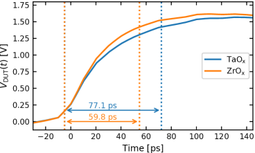
In [1], we have demonstrated for the TaOx-based device a charging time of 77.1 ps by using its scattering parameters. In Fig. S1, we have plotted the scattering parameters of both, the TaOx and ZrOx-based device. The forward reflection is shown in (a) and the forward transmission in (b). They were measured with a HP8722ES vector network analyser (VNA) in the frequency range from 50 MHz to 40 GHz at a power of -3 dBm. The VNA was calibrated using the SOLT (short-open-load-trough) method with a calibration substrate (FormFactor CSR-8 100-250). Both devices were driven to the HRS prior to the frequency domain measurements and show a similar trend over the entire frequency range. Both are insulating at low frequencies and become transparent at higher frequencies. This is due to the capacitance of the VCM stack, which acts as high pass filter.
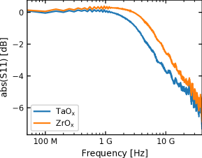
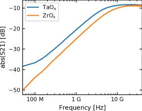
From the scatterings parameters, we determined the electrical charging time, by using the method described in [1]. The voltage at the device is the sum of the applied signal and the reflected signal , minus the transmitted signal :
| (1) |
An 250 ps pulse with an amplitude of 0.8 V was used as , having a rise time of about 35 ps (10 %-90 %). The reflected and transmitted signals were calculated by building the Fourier transform of , multiplying it with for the reflection or with for the transmission, and finally building the inverse Fourier transform of this product:
| (2) |
| (3) |
The results for of both devices are shown in Fig. S2, showing that both devices can be charged in less than 80 ps (10 %-90 %). Please note that rises to twice the amplitude of , which is due to the superposition of the incoming and reflected pulse. For this reason, we indicated always twice the pulse’s amplitude in the main text.
S.2 RESET failure of TaOx-based device at = 1.8 V
The current response of the TaOx-based device to a 4 ns pulse with an amplitude of 1.8 V is shown in Fig. S3. The devices was driven to a LRS of 1.31 k before the pulse’s application. Although, a positive voltage pulse (applied to the active Pt electrode) should drive the device to the HRS, the device’s resistance decreased to 990 , remaining in the LRS. Also, the current was significantly higher than during pulses with lower amplitude. At a pulse amplitude of 1.6 V (see Fig. 2(a) of the main text), the maximum current amounted to approx. 1.5 mA and then decreased abruptly. In the case of 1.8 V it remained constantly at approx. 3 mA. This current increase can be explained by the occurrence of a unipolar SET event, which in this case prohibits a successful RESET operation. In a previous study on the RESET kinetics of a similar TaOx-based device, only a small linear dependence of the maximum current on the applied voltage was observed [2]. The observed current increase from 1.5 mA to 3.0 mA can, therefore, not be explained by the increase of voltage from 1.6 V to 1.8 V.
S.3 RESET kinetics
Fig. 3(c) of the main text shows the median values of the ratio / of the TaOx- and ZrOx-based device, which measured during the RESET kinetics in the time regime from 250 ps to 50 ps. Two pulse amplitudes were used (1.6 V and 2.2 V). The boxplot representation was only shown for the TaOx-based device at 1.6 V in Fig. 3(b). The boxplot representation of the other three measurements is shown in Fig. S4. As the ratio / does not yield any information about the absolute resistance values, the boxplots of are shown in Fig. S5. The values were always in the range between 1.0 k and 2.5 k.


S.4 Unipolar SET – Kinetics
Fig. 4(c) of the main text shows the median values of the ratio / of the TaOx- and ZrOx-based device, which measured during the unipolar SET kinetics in the time regime from 250 ps to 50 ps. Four different pulse amplitudes were used, ranging from 1.6 V to 5.0 V. The boxplot representation was only shown for the TaOx-based device at 3.2 V in Fig. 4(b). The boxplot representation of the other measurements on the TaOx- and ZrOx-based device are shown in Fig. S6 and Fig. S7, respectively. The boxplots of are shown in Fig. S8 and Fig. S9 for the TaOx- and the ZrOx-based device, respectively. The values were always in the range between 10 k and 30 k. The measurement cycle was repeated at least 10 times and until smooth lines for / were achieved. The number of conducted cycles are listed in Table S1. In Fig. S10 transient current responses to 50 ps long pulses are shown for both devices. The devices switched from the HRS to the LRS during theses pulses.


| Device | Voltage [V] | No. of cycles |
|---|---|---|
| TaOx | 2.2 | 100 |
| TaOx | 3.2 | 300 |
| TaOx | 5.0 | 100 |
| ZrOx | 1.6 | 300 |
| ZrOx | 2.2 | 300 |
| ZrOx | 3.2 | 500 |
| ZrOx | 5.0 | 100 |
S.5 Unipolar SET – Endurance
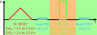
The measurement procedure to test the devices’ endurance is sketched in Fig. S11(a). All applied voltages were positive (including the read-out). At the beginning of each cycle, the device is driven into the HRS with a positive voltage sweep with an amplitude of 1.3 V for the TaOx- and of 1.2 V for the ZrOx-based device. The amplitude was reduced compared to the measurement in the main text to reduce the stress onto the devices. To reduce the measurement duration, the sweep rate was also accelerated from 0.5 V/s to 2.5 V/s. The devices were then driven into the LRS with a positive voltage pulse. For the TaOx-based device, the pulse width was chosen to 70 ps and the pulse amplitude to 5.0 V. For the ZrOx-based device, the pulse width was chosen to 50 ps and the pulse amplitude to 7.1 V. The devices’ resistances were read at a voltage of 0.5 V, before and after the pulse’s application.
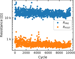
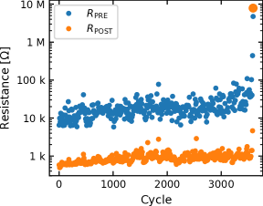
The results are shown in Fig. S11(b) and (c) for the TaOx- and ZrOx-based device, respectively. The measurement of the TaOx-based device was aborted after 104 cycles. The and were always separated by an order of magnitude and an even higher endurance may be possible. The ZrOx-based device got stuck in the HRS after 3590 cycles. Until then, the and were also separated by one order of magnitude. The device could, however, be driven back to the LRS with a negative voltage sweep and was again operational. Further adjustments of the pulse width and amplitude may result in an higher endurance, but this is beyond the scope of this study.
References
- [1] M. von Witzleben, S. Walfort, R. Waser, S. Menzel, and U. Böttger. Determining the electrical charging speed limit of reram devices. IEEE J. Electron Devices Soc., 9:667–678, 2021. doi:10.1109/JEDS.2021.3095389.
- [2] A. Marchewka, B. Roesgen, K. Skaja, H. Du, C. L. Jia, J. Mayer, V. Rana, R. Waser, and S. Menzel. Nanoionic Resistive Switching Memories: On the Physical Nature of the Dynamic Reset Process. Adv. Electron. Mater., 2(1):1500233/1–13, 2016. doi:10.1002/aelm.201500233.